
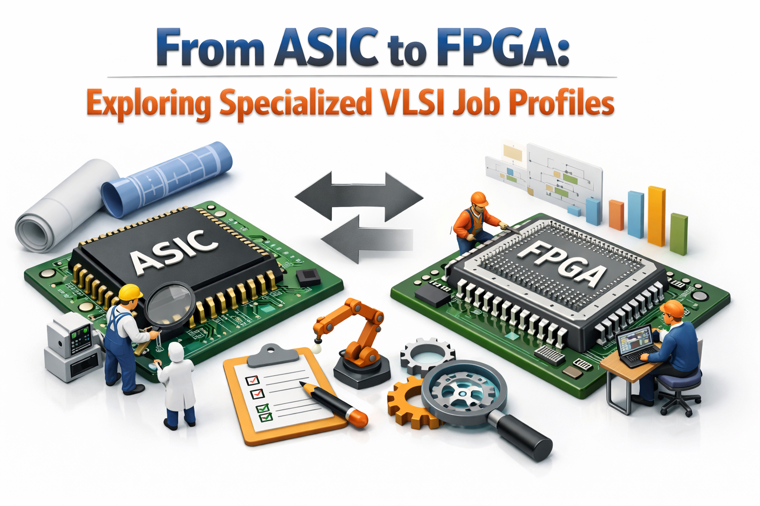
From ASIC to FPGA: Exploring Specialized VLSI Job Profiles
Navigate through this article using the table of contents below
Table of Contents
No headings found in this article.
The semiconductor industry is evolving rapidly, and specialized VLSI job roles are becoming more important than ever. From designing Application-Specific Integrated Circuits (ASICs) to developing flexible and reconfigurable Field-Programmable Gate Arrays (FPGAs), engineers today have multiple career paths within the VLSI ecosystem. Understanding the differences between ASIC and FPGA technologies—and the job profiles associated with them—can help aspiring engineers choose the right specialization. As the demand for advanced chips grows across industries like AI, automotive, 5G, and consumer electronics, professionals with expertise in these domains are highly sought after.
In this blog, we explore specialized VLSI job profiles ranging from ASIC design and verification engineers to FPGA developers and system architects. Each role requires a unique combination of digital design knowledge, hardware description languages such as Verilog or VHDL, and familiarity with industry-standard EDA tools. By understanding the responsibilities, skills, and career opportunities associated with ASIC and FPGA development, beginners and professionals can better navigate the semiconductor industry and identify the right path to build a successful career in VLSI design.
Introduction to ASIC and FPGA in VLSI Design
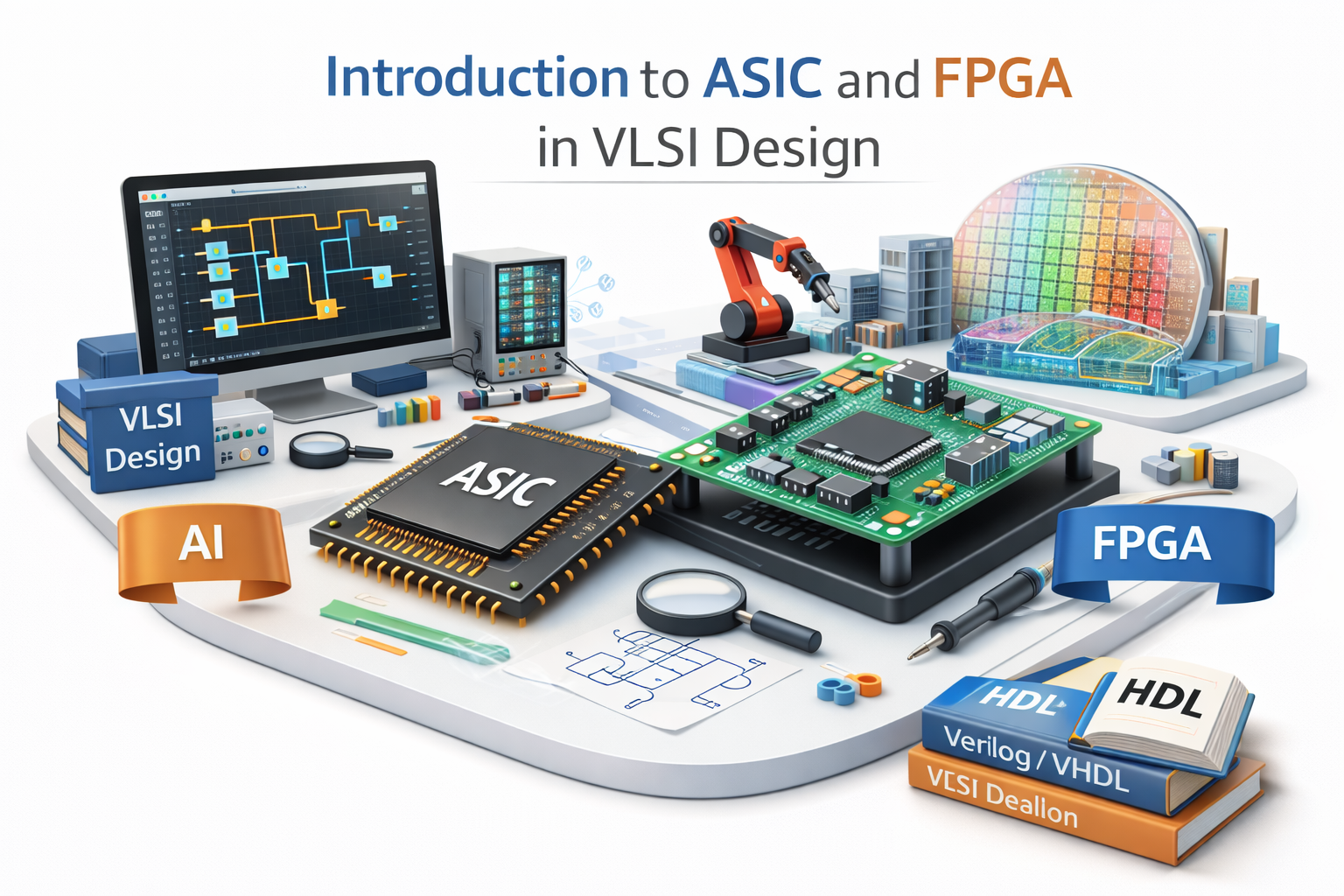
Application-Specific Integrated Circuits (ASICs) and Field-Programmable Gate Arrays (FPGAs) are two important technologies used in modern VLSI (Very Large Scale Integration) design for developing advanced semiconductor chips. Both ASIC and FPGA architectures are widely used to implement complex digital systems such as processors, communication modules, AI accelerators, and embedded systems. While ASICs are custom-designed chips optimized for a specific function, FPGAs are reconfigurable devices that allow designers to program and modify hardware logic even after manufacturing. Understanding these two technologies is essential for engineers who want to build a career in the semiconductor and VLSI design industry.
ASIC design focuses on creating a dedicated integrated circuit tailored for a particular application, which results in high performance, low power consumption, and optimized silicon area. Because ASIC chips are manufactured for a specific purpose, they are widely used in applications such as smartphones, automotive electronics, networking equipment, and consumer devices. However, the ASIC development process involves a complex design flow including RTL design, functional verification, synthesis, physical design, and chip fabrication, which makes it costly and time-consuming compared to other solutions.
In contrast, FPGAs provide a flexible platform where hardware logic can be programmed and reconfigured using hardware description languages like Verilog or VHDL. This flexibility makes FPGAs ideal for rapid prototyping, hardware testing, research, and applications that require frequent updates or customization. FPGA technology is commonly used in fields such as telecommunications, aerospace, defense systems, and AI acceleration. In the VLSI ecosystem, both ASIC and FPGA technologies play complementary roles, giving engineers multiple specialization paths and creating diverse career opportunities in digital design, verification, and hardware development.
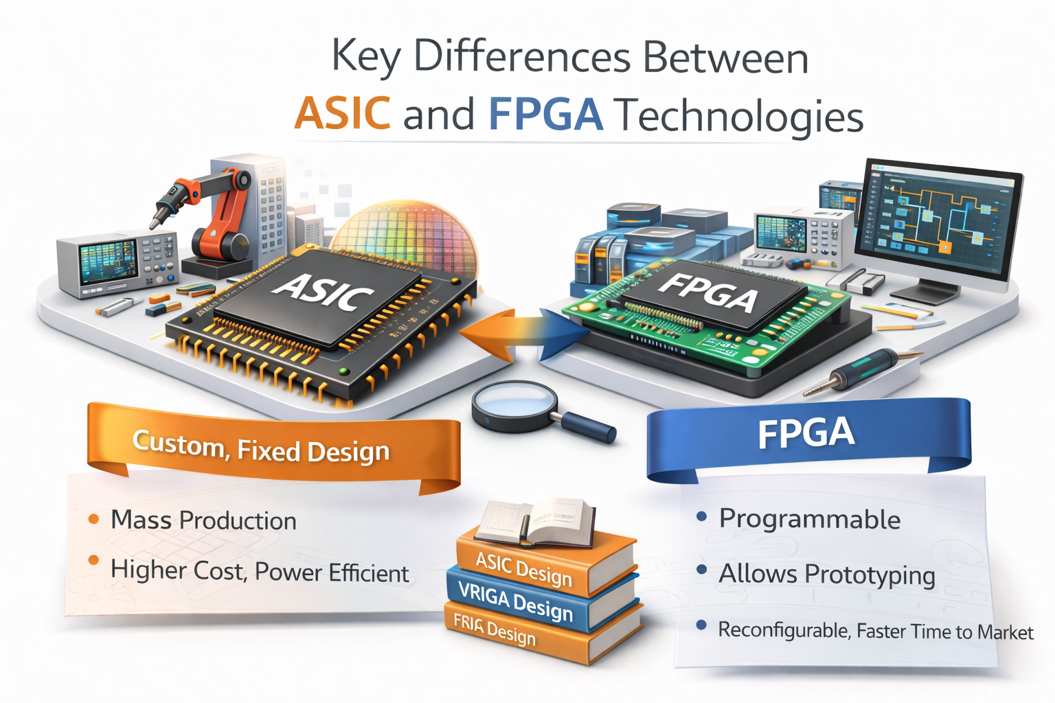
Key Differences Between ASIC and FPGA Technologies
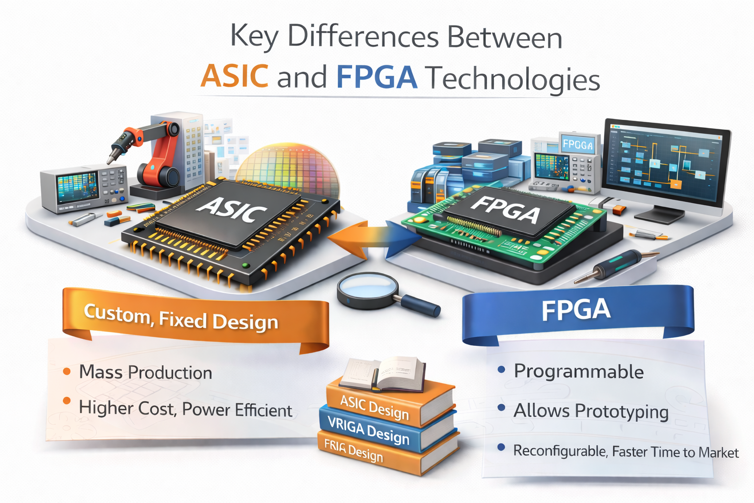
ASIC (Application-Specific Integrated Circuit) and FPGA (Field-Programmable Gate Array) technologies differ mainly in their design flexibility, performance, and development approach within the VLSI design ecosystem. An ASIC is a custom-designed chip created for a specific application or function, which means the hardware architecture is fixed once the chip is manufactured. Because of this specialization, ASICs typically offer higher performance, lower power consumption, and optimized silicon area, making them ideal for mass-produced products such as smartphones, automotive controllers, networking devices, and high-performance processors. However, ASIC development requires a complex and costly design flow that includes RTL design, verification, synthesis, physical design, and fabrication, making it more suitable for large-scale production.
In contrast, FPGAs are reconfigurable semiconductor devices that allow designers to program and modify the hardware logic even after the chip has been manufactured. This flexibility enables engineers to test designs quickly, implement prototypes, and update hardware functionality without producing a new chip. FPGAs are widely used in applications such as prototyping ASIC designs, telecommunications systems, aerospace technologies, and AI hardware acceleration. Although FPGAs provide faster development cycles and design flexibility, they generally consume more power and offer lower performance compared to ASICs. Understanding these differences helps engineers choose the right technology depending on factors like cost, scalability, performance requirements, and development time.
Overview of the VLSI Design Flow for ASIC and FPGA Development
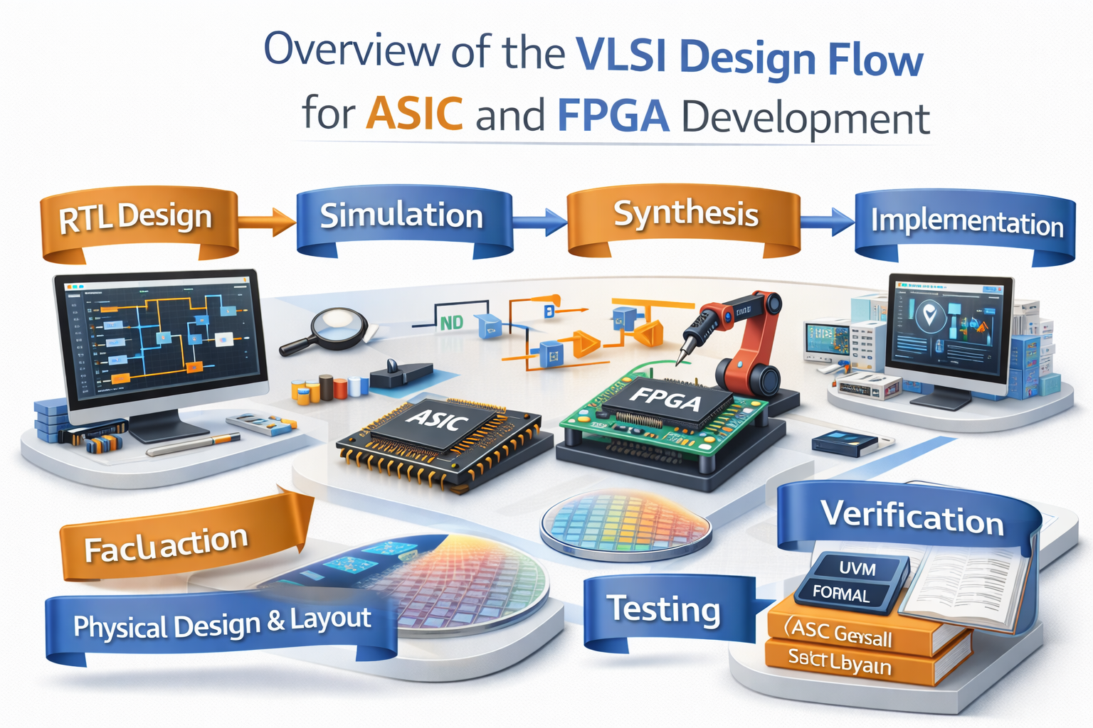
The VLSI design flow is a structured process used to transform a system specification into a functional semiconductor chip or programmable hardware device. Both ASIC and FPGA development follow similar front-end design stages, beginning with system specification and architecture design, where engineers define the functionality, performance requirements, and hardware structure of the circuit. This is followed by RTL (Register Transfer Level) design, where engineers describe the hardware logic using hardware description languages such as Verilog or VHDL. The RTL code is then tested using simulation tools to verify the functional correctness of the design before moving to later stages.
After RTL verification, the next step in the VLSI design flow is logic synthesis, where the HDL code is converted into a gate-level representation using EDA tools. For ASIC development, the synthesized design goes through additional backend stages such as floorplanning, placement, routing, clock tree synthesis, and timing analysis, which collectively form the physical design process. These steps ensure that the chip layout is optimized for power, performance, and area before it proceeds to fabrication in semiconductor manufacturing facilities.
In FPGA development, the flow is slightly different after synthesis. Instead of going through full custom physical design, the synthesized logic is mapped onto the configurable resources of an FPGA device through processes called mapping, placement, and routing using FPGA-specific tools like Xilinx Vivado or Intel Quartus. Once the design is implemented and validated, a configuration bitstream is generated and programmed into the FPGA chip. This flexible development flow allows engineers to modify and update designs quickly, making FPGAs particularly useful for prototyping and rapid hardware development in modern VLSI systems.
ASIC Design Engineer: Roles and Responsibilities
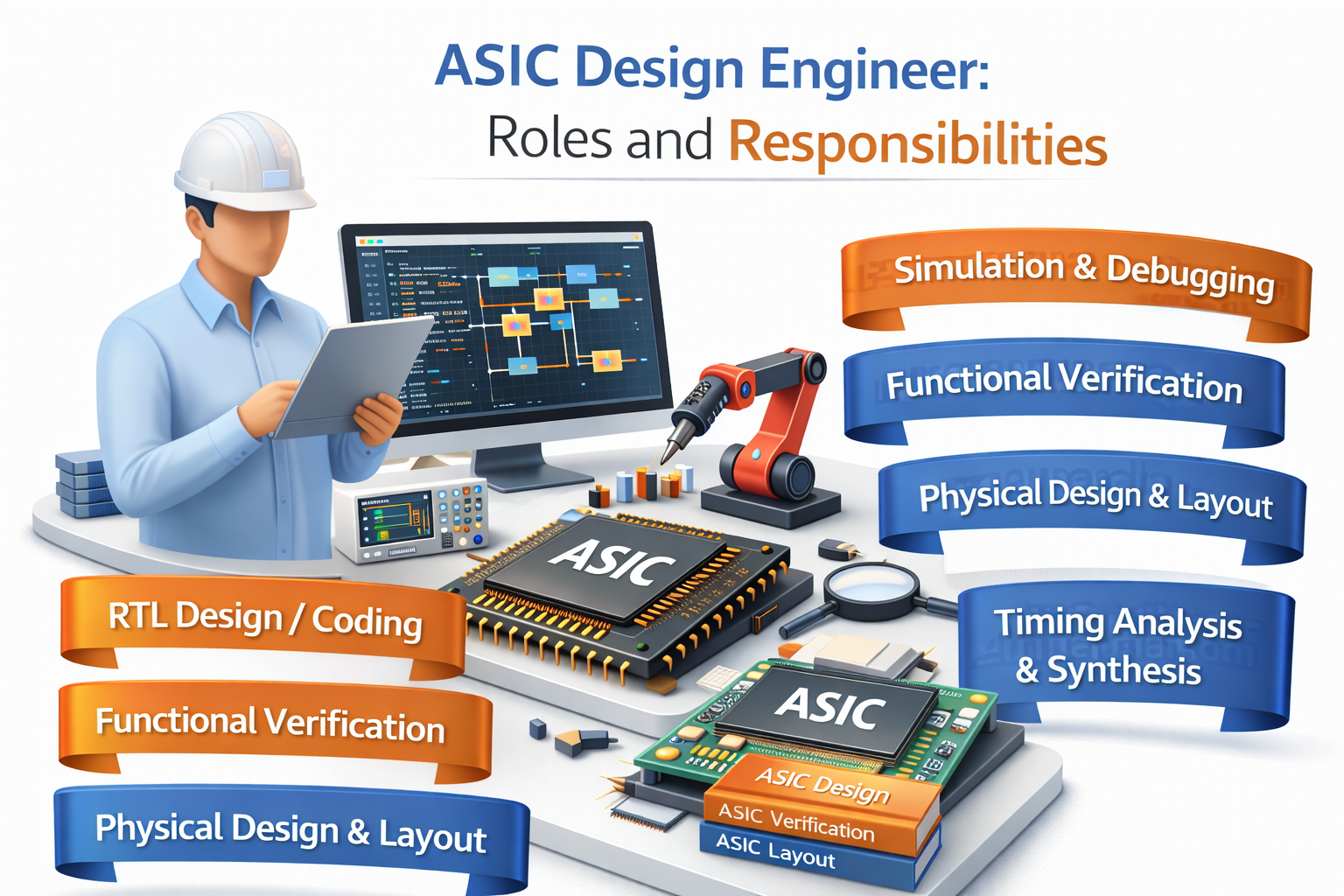
An ASIC Design Engineer is responsible for designing and developing application-specific integrated circuits that perform dedicated functions in electronic systems. The role typically begins with understanding system requirements and translating them into digital logic architecture and RTL (Register Transfer Level) designs using hardware description languages such as Verilog or VHDL. ASIC design engineers focus on creating efficient digital circuits while optimizing important parameters like performance, power consumption, and chip area. They also work closely with system architects and verification engineers to ensure that the design meets functional and technical specifications.
In addition to RTL development, ASIC design engineers participate in multiple stages of the VLSI design flow, including functional simulation, synthesis, timing analysis, and design optimization. They collaborate with verification teams to debug design issues and ensure the correctness of the chip before it moves to the physical design stage. Engineers in this role must also be familiar with industry-standard EDA tools from companies like Synopsys, Cadence, and Siemens EDA, as well as scripting languages such as Python or TCL for automation. With the growing demand for high-performance chips in areas like AI, automotive electronics, and data centers, ASIC design engineers play a crucial role in building the next generation of semiconductor technologies.
FPGA Design Engineer: Roles and Responsibilities
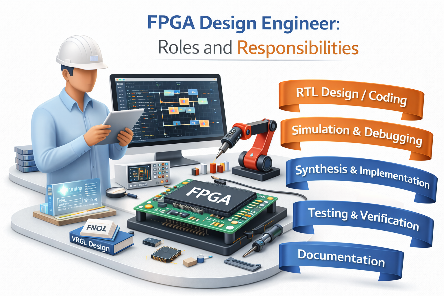
An FPGA Design Engineer specializes in developing digital hardware systems using Field-Programmable Gate Arrays (FPGAs), which are reconfigurable semiconductor devices that allow engineers to implement and modify hardware logic after manufacturing. The primary responsibility of an FPGA engineer is to design and implement digital circuits using hardware description languages (HDLs) such as Verilog or VHDL. They work on tasks such as system architecture design, RTL coding, simulation, and debugging to ensure that the hardware logic performs the intended function. FPGA engineers are often involved in rapid prototyping, hardware acceleration, and system validation before designs move toward ASIC implementation.
In addition to RTL design, FPGA engineers handle tasks like synthesis, place and route, timing analysis, and bitstream generation using specialized FPGA development tools such as Xilinx Vivado or Intel Quartus. They also collaborate with software and hardware teams to integrate FPGA-based systems into larger embedded platforms. FPGA design engineers are commonly involved in industries such as telecommunications, aerospace, defense, data centers, and artificial intelligence, where flexible and high-performance hardware solutions are required. Their role is critical in enabling faster development cycles, hardware testing, and innovation in modern digital systems.
Key Skills Required for ASIC and FPGA Engineers
To succeed as an ASIC or FPGA engineer, a strong foundation in digital electronics and VLSI design principles is essential. Engineers must understand concepts such as combinational and sequential logic, finite state machines, timing analysis, and digital circuit optimization. Knowledge of hardware description languages (HDLs) like Verilog, SystemVerilog, or VHDL is critical because these languages are used to design and describe digital hardware at the RTL (Register Transfer Level). A deep understanding of computer architecture and digital system design also helps engineers build efficient and scalable hardware solutions.
Another important skill for ASIC and FPGA engineers is proficiency with Electronic Design Automation (EDA) tools used throughout the VLSI design flow. Engineers working on ASIC development often use tools from Synopsys, Cadence, and Siemens EDA for tasks such as simulation, synthesis, verification, and physical design. FPGA engineers typically work with platform-specific tools like Xilinx Vivado and Intel Quartus for synthesis, placement, routing, and hardware implementation. In addition, knowledge of scripting languages such as Python, Perl, or TCL is valuable for automating design processes and improving workflow efficiency.
Apart from technical expertise, ASIC and FPGA engineers must also possess problem-solving skills, debugging abilities, and a strong understanding of system-level design. Collaboration and communication skills are equally important because VLSI development involves working with multiple teams including verification engineers, physical design engineers, and system architects. As semiconductor technologies continue to evolve in fields such as AI hardware, 5G communication, automotive electronics, and high-performance computing, engineers who continuously upgrade their skills and stay updated with new design methodologies will have strong career opportunities in the VLSI industry.
Educational Background and Certifications for VLSI Careers
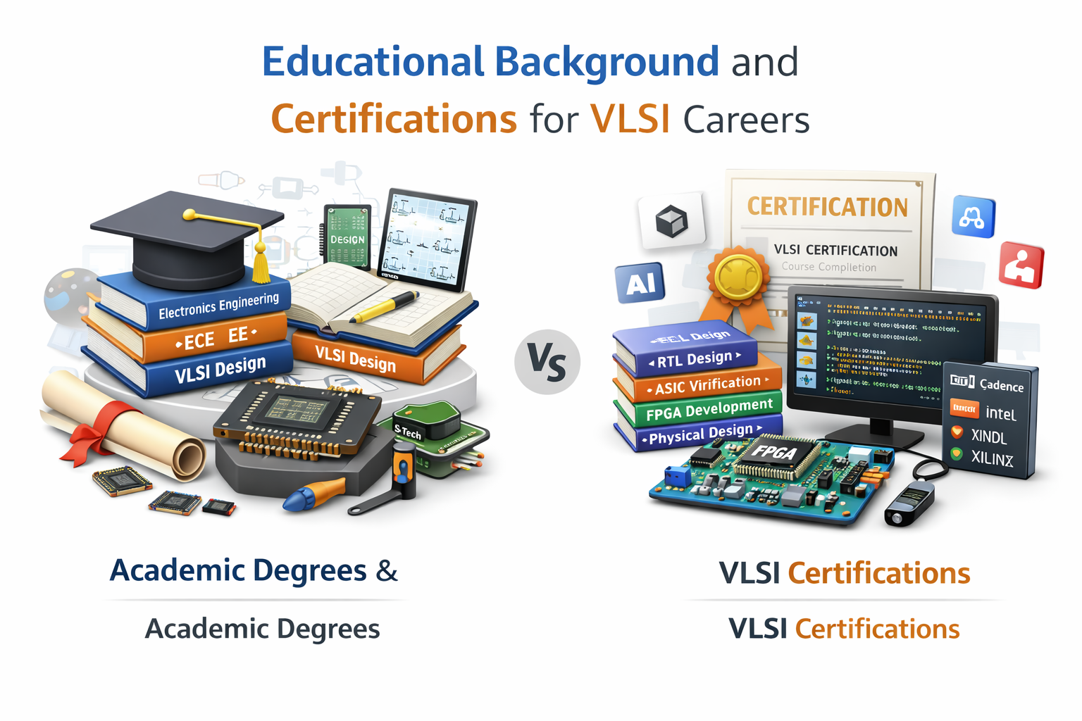
A strong educational foundation is essential for building a successful career in the VLSI (Very Large Scale Integration) industry. Most professionals in this field hold a Bachelor’s degree in Electronics and Communication Engineering (ECE), Electrical Engineering (EE), Electronics Engineering, or related disciplines. During their academic studies, students typically learn important subjects such as digital electronics, semiconductor physics, microelectronics, CMOS technology, computer architecture, and embedded systems, which form the core knowledge required for VLSI design. Many engineers also pursue a Master’s degree (M.Tech or MS) in VLSI Design, Microelectronics, or Semiconductor Technology to gain deeper expertise and improve their chances of securing advanced roles in the semiconductor industry.
In addition to formal education, specialized VLSI training programs and certifications can significantly enhance job prospects and practical skills. Certification courses in areas such as RTL design, ASIC verification, FPGA development, and physical design provide hands-on experience with hardware description languages like Verilog, VHDL, and SystemVerilog, along with exposure to industry-standard EDA tools from Synopsys, Cadence, and Mentor Graphics. Many aspiring engineers also build practical experience by working on FPGA projects, chip design simulations, and open-source hardware platforms. Combining academic knowledge with industry-focused certifications and real-world projects helps candidates build a strong profile and increases their chances of entering the competitive VLSI and semiconductor job market.
Best Projects to Build a Strong ASIC or FPGA Engineer Resume
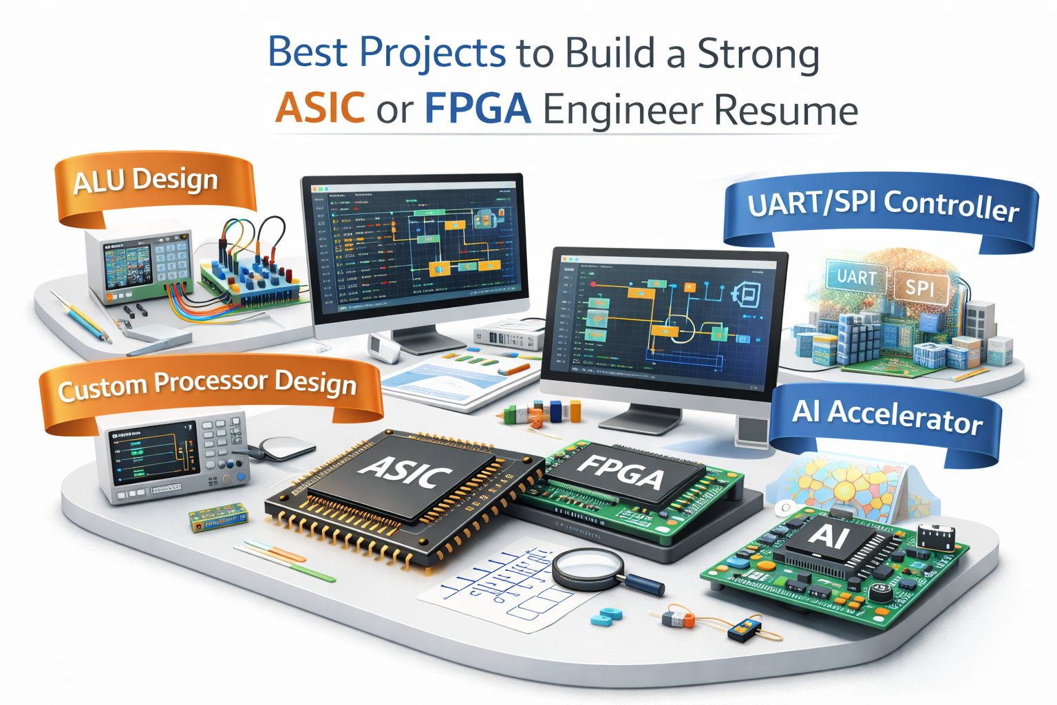
Building practical projects is one of the most effective ways to strengthen an ASIC or FPGA engineer resume and demonstrate real-world design skills to potential employers. Projects allow engineers to apply concepts from digital electronics, RTL design, and hardware description languages such as Verilog or VHDL to create functional hardware systems. Recruiters in the semiconductor industry often look for candidates who have hands-on experience with design, simulation, and debugging. Simple projects like ALU (Arithmetic Logic Unit) design, traffic light controllers, or finite state machine implementations help beginners understand digital logic design and RTL development.
Intermediate-level projects focus on implementing more complex hardware modules that reflect real VLSI design workflows. Examples include designing a UART communication controller, SPI interface, or a simple RISC-based processor using Verilog or VHDL. These projects usually involve multiple stages such as RTL coding, simulation, synthesis, and functional verification using industry-style methodologies. Implementing these designs on an FPGA board allows engineers to gain experience with hardware testing and understand how digital logic interacts with real systems.
Advanced projects can significantly enhance a resume by demonstrating deeper expertise in ASIC or FPGA development. Examples include building an FPGA-based image processing system, AI accelerator module, hardware cryptography engine, or custom digital IP core. These projects often require integration of multiple hardware modules, optimization for performance, and use of EDA tools for synthesis and implementation. Completing such projects not only strengthens technical skills but also shows employers that the candidate has practical experience with real semiconductor design challenges, which is highly valuable in VLSI job roles.
Future Scope of ASIC and FPGA Careers in the Semiconductor Industry
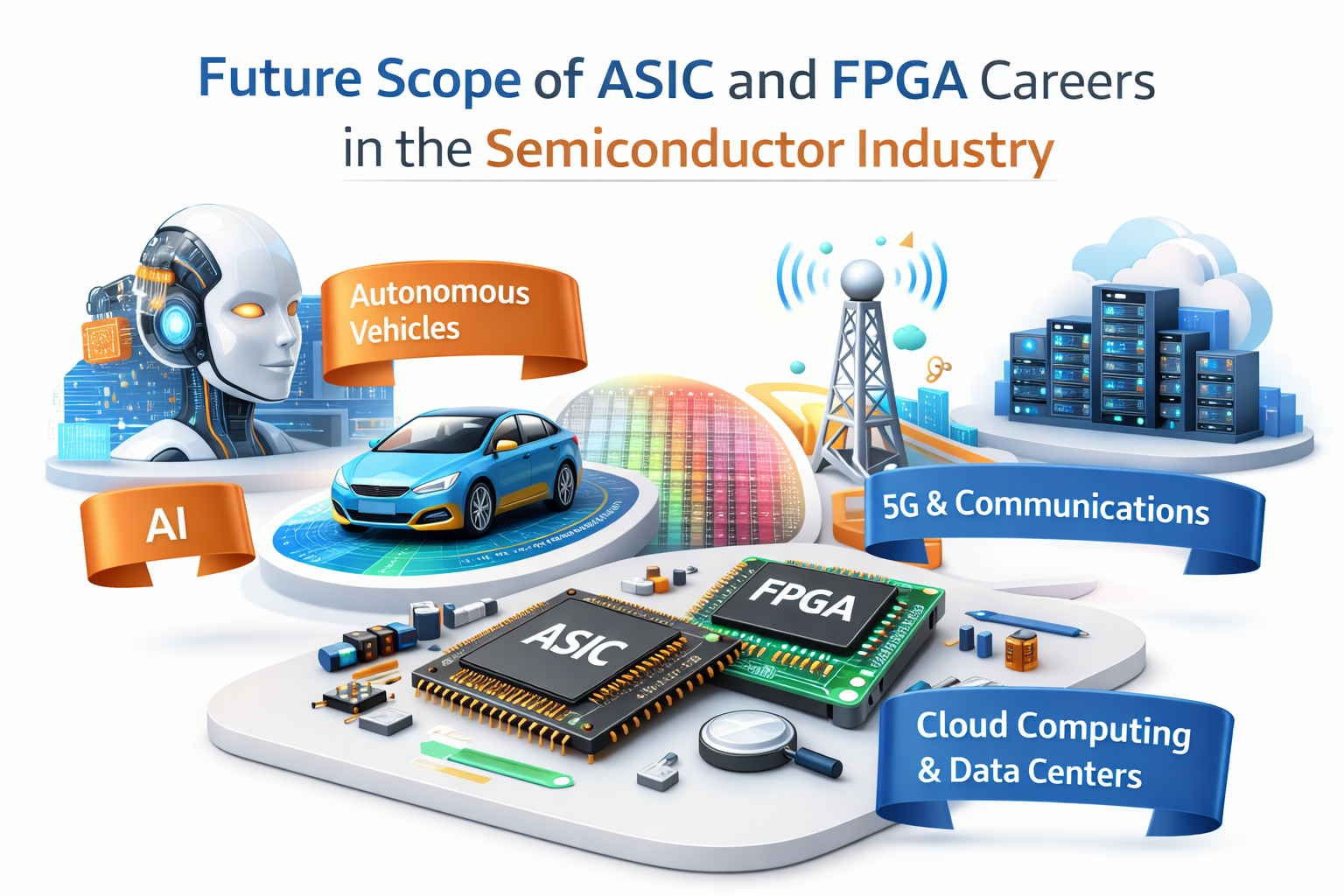
The future of ASIC and FPGA careers in the semiconductor industry is extremely promising as the demand for high-performance and specialized chips continues to grow across multiple technology sectors. Industries such as artificial intelligence (AI), 5G communication, autonomous vehicles, cloud computing, and data centers require advanced semiconductor solutions that deliver higher speed, lower power consumption, and improved efficiency. ASIC engineers play a critical role in designing custom chips optimized for specific applications like AI accelerators, mobile processors, and networking hardware, while FPGA engineers contribute by developing flexible hardware platforms used for rapid prototyping, hardware acceleration, and system validation.
As global investment in semiconductor manufacturing and chip design increases, companies are actively seeking skilled professionals with expertise in VLSI design, RTL development, verification, and hardware architecture. FPGAs are also gaining popularity in fields such as edge computing, defense systems, and real-time data processing, where reconfigurable hardware provides significant advantages. With emerging technologies like advanced node semiconductor fabrication, heterogeneous computing, and AI-driven chip design, the demand for ASIC and FPGA engineers is expected to rise steadily in the coming years. For aspiring engineers, building strong technical skills and hands-on project experience can open doors to highly rewarding and future-proof careers in the semiconductor industry.
Tips for Beginners to Start a Career in ASIC or FPGA Design
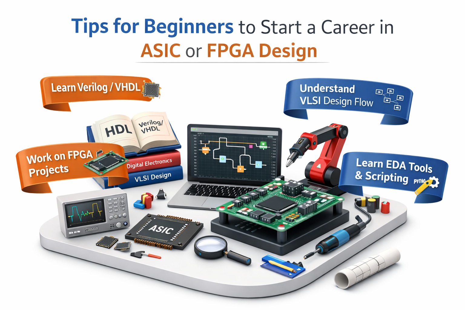
Starting a career in ASIC or FPGA design requires building a strong foundation in digital electronics, computer architecture, and VLSI design fundamentals. Beginners should focus on learning key concepts such as combinational and sequential logic, finite state machines, timing analysis, and hardware architecture. It is also essential to gain proficiency in hardware description languages (HDLs) like Verilog, SystemVerilog, or VHDL, which are widely used for RTL design in semiconductor development. Along with theoretical knowledge, understanding the complete VLSI design flow—from RTL design and simulation to synthesis and implementation— helps beginners develop a clear picture of how digital circuits are transformed into real hardware.
Practical experience plays a crucial role in entering the VLSI industry. Beginners should work on hands-on projects using FPGA boards, build small digital systems such as communication controllers or processors, and practice simulation and debugging using industry tools. Learning to use EDA tools and scripting languages like Python or TCL can also improve productivity and automation skills. Additionally, participating in internships, VLSI training programs, and open-source hardware projects can help build a strong portfolio. By consistently improving technical skills and staying updated with semiconductor technologies, beginners can successfully start and grow a career in ASIC or FPGA design.
Conclusion
The world of VLSI design offers a wide range of specialized career opportunities, and roles in ASIC and FPGA development are among the most important in the semiconductor industry. From designing high-performance custom chips to developing flexible and reconfigurable hardware platforms, these technologies play a crucial role in powering modern electronics such as smartphones, AI systems, automotive electronics, and communication networks. Understanding the differences between ASIC and FPGA technologies, along with the various job profiles associated with them, helps aspiring engineers identify the right specialization and build a clear career path in the VLSI domain.
As the demand for advanced semiconductor solutions continues to grow, professionals with strong skills in digital design, hardware description languages, verification methodologies, and EDA tools will remain highly valuable in the industry. By gaining the right educational background, working on practical projects, and continuously upgrading technical knowledge, beginners can position themselves for successful careers in ASIC and FPGA engineering. With the rapid expansion of technologies like AI, 5G, and high-performance computing, the future of VLSI careers looks promising for engineers ready to innovate and contribute to the next generation of semiconductor technology.