

How AI & Deep Learning can Boosts Advanced Electronics Design and improve performance
Navigate through this article using the table of contents below
Table of Contents
No headings found in this article.
What if your electronic systems could design themselves—faster, smarter, and more efficiently than ever before? How AI & Deep Learning Can Boost Advanced Electronics Design and Improve Performance is no longer a futuristic concept but a transformative reality reshaping the semiconductor and embedded systems landscape. Artificial Intelligence (AI) and Deep Learning (DL) are revolutionizing advanced electronics design by automating complex tasks such as circuit optimization, layout generation, power analysis, and performance validation. From predictive modeling in VLSI design to intelligent simulation workflows, AI-driven methodologies are significantly reducing development cycles while enhancing accuracy and scalability.
In today’s competitive electronics industry, performance, power efficiency, and time-to-market are critical success factors. AI-powered design automation tools leverage data-driven algorithms to optimize RTL architectures, improve signal integrity, enhance thermal management, and minimize power consumption. Deep learning models can analyze massive design datasets, identify hidden patterns, and predict potential failures before fabrication, reducing costly re-spins. By integrating AI into EDA workflows, engineers can achieve higher reliability, faster prototyping, and superior system-level optimization—ultimately driving innovation in advanced electronics systems and next-generation semiconductor technologies.
Introduction to AI and Deep Learning in Electronics Design

Artificial Intelligence (AI) and Deep Learning (DL) are rapidly transforming the landscape of electronics design by introducing data-driven intelligence into traditionally algorithmic workflows. In advanced electronics and semiconductor engineering, design complexity has increased exponentially due to shrinking technology nodes, multi-core architectures, and high-performance computing requirements. Conventional Electronic Design Automation (EDA) approaches rely heavily on rule-based systems and manual optimization, which can be time-consuming and computationally intensive. AI enhances these processes by leveraging machine learning models to analyze vast design datasets, identify optimization opportunities, and automate decision-making in areas such as circuit synthesis, placement, routing, and timing analysis.
Deep learning, a subset of AI that uses neural networks with multiple hidden layers, plays a critical role in predictive modeling and pattern recognition within electronics design. By training on historical silicon data, simulation results, and layout configurations, deep learning models can accurately forecast power consumption, signal integrity issues, thermal hotspots, and performance bottlenecks before fabrication. This predictive capability significantly reduces costly design re-spins and shortens verification cycles. Moreover, AI-driven analytics enable intelligent trade-off analysis between power, performance, and area (PPA), which is a core objective in modern VLSI and SoC development.
The integration of AI and deep learning into electronics design workflows also supports faster innovation and improved scalability. Engineers can now utilize AI-powered tools for automated testbench generation, fault detection, yield prediction, and rapid prototyping. As semiconductor devices continue to scale toward advanced nanometer technologies, the role of AI becomes increasingly strategic rather than supplementary. By embedding intelligence directly into EDA ecosystems, organizations can achieve higher design accuracy, reduced time-to-market, and superior system-level optimization—establishing AI as a foundational technology in next-generation electronics engineering.
How AI is Transforming Advanced VLSI and Chip Design

Artificial Intelligence (AI) is fundamentally transforming advanced VLSI and chip design by introducing intelligent automation into traditionally complex and iterative design flows. In modern nanometer-scale technologies, achieving optimal Power, Performance, and Area (PPA) requires analyzing millions of design variables across RTL coding, logic synthesis, floorplanning, placement, and routing. AI-driven algorithms enhance these stages by learning from historical silicon data and simulation results to predict congestion, timing violations, and power inefficiencies early in the design cycle. Machine learning models can recommend optimized cell placement strategies, improve clock tree synthesis, and accelerate timing closure—significantly reducing manual intervention and engineering turnaround time.
Beyond optimization, AI is enabling predictive and adaptive chip design methodologies. Deep learning models assist in identifying design rule violations, signal integrity risks, and electromigration issues before tape-out, minimizing costly re-spins. AI-powered tools can also automate design space exploration by evaluating thousands of architectural configurations in parallel, selecting the most efficient microarchitecture for specific workloads such as AI accelerators, 5G processors, or automotive SoCs. As chip complexity continues to grow with heterogeneous integration and advanced packaging technologies, AI is shifting VLSI design from a reactive debugging process to a proactive, data-driven engineering discipline that enhances productivity, reliability, and overall silicon performance.
AI-Powered Electronic Design Automation (EDA) Tools
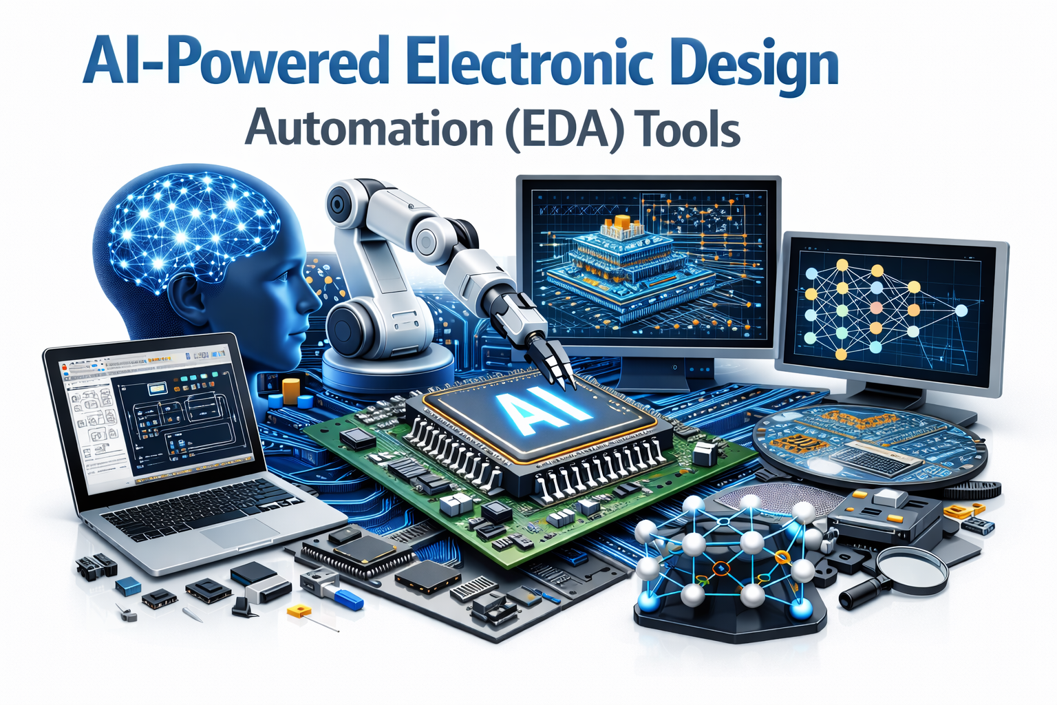
AI-powered Electronic Design Automation (EDA) tools are redefining how complex semiconductor systems are designed, verified, and optimized. Traditional EDA workflows rely on deterministic algorithms and rule-based heuristics to handle synthesis, placement, routing, and verification tasks. However, as technology nodes shrink to advanced nanometer scales and chip architectures grow increasingly heterogeneous, these conventional approaches face scalability and runtime limitations. By integrating Artificial Intelligence (AI) and machine learning models, modern EDA tools can analyze massive historical design datasets, learn from prior silicon implementations, and deliver data-driven optimization strategies that significantly improve efficiency and design accuracy.
One of the most impactful applications of AI in EDA tools is intelligent optimization during physical design and timing closure. Machine learning algorithms can predict routing congestion, power density hotspots, and signal integrity violations early in the design cycle. This predictive capability enables automated floorplanning, adaptive placement strategies, and faster convergence during static timing analysis (STA). AI-powered EDA platforms also enhance verification workflows by detecting functional bugs, generating smarter test patterns, and improving coverage analysis. As a result, engineers experience shorter simulation runtimes, reduced iteration cycles, and improved Power, Performance, and Area (PPA) outcomes.
Furthermore, AI-driven EDA tools are enabling advanced design space exploration and faster time-to-market for complex SoCs and application-specific integrated circuits (ASICs). Instead of manually evaluating multiple architectural trade-offs, AI engines can simultaneously assess thousands of configurations to identify the most optimal solution based on workload requirements. This capability is particularly critical for emerging domains such as AI accelerators, high-speed networking chips, and automotive electronics. By embedding machine learning intelligence directly into EDA ecosystems, semiconductor companies can enhance productivity, reduce costly design re-spins, and maintain competitiveness in an increasingly performance-driven electronics industry.
Deep Learning for Circuit Optimization and Performance Enhancement

Deep learning is playing a transformative role in circuit optimization and performance enhancement by introducing advanced predictive modeling and pattern recognition into the electronics design workflow. Modern integrated circuits contain billions of transistors, making manual optimization across parameters such as timing, power consumption, and area increasingly complex. Deep neural networks (DNNs) can be trained on historical layout data, simulation reports, and silicon validation results to predict circuit behavior under varying operating conditions. This enables early identification of timing violations, voltage drops, leakage currents, and thermal hotspots—allowing engineers to implement corrective measures before physical fabrication. As a result, deep learning significantly improves Power, Performance, and Area (PPA) optimization in advanced VLSI and SoC design.
Beyond predictive analysis, deep learning enhances automated design space exploration and microarchitectural tuning. Instead of relying solely on heuristic-based optimization algorithms, neural networks can evaluate thousands of design configurations in parallel and recommend the most efficient architecture for specific performance targets. For example, deep learning models can optimize transistor sizing, buffer insertion, clock tree balancing, and interconnect routing to minimize latency while maintaining power efficiency. This data-driven approach accelerates convergence during synthesis and physical design stages, reduces costly re-spins, and enables higher overall silicon reliability. By embedding deep learning into circuit design workflows, semiconductor companies can achieve faster innovation cycles and superior system-level performance in next-generation electronics.
AI-Driven Simulation and Verification Techniques

AI-driven simulation and verification techniques are transforming the way modern semiconductor designs are validated before fabrication. As VLSI and SoC architectures grow more complex, traditional verification methodologies—such as constrained random testing and rule-based simulation—struggle to achieve full functional coverage within practical timelines. Artificial Intelligence (AI) enhances these workflows by leveraging machine learning models to analyze historical bug databases, waveform patterns, and regression results. This enables predictive identification of high-risk design areas, allowing verification teams to prioritize critical test scenarios and significantly reduce simulation cycles while improving overall coverage efficiency.
One of the most powerful applications of AI in hardware verification is intelligent testbench generation and automated bug detection. Machine learning algorithms can study previous design failures to generate targeted test vectors that expose corner-case issues more effectively than purely random stimulus methods. AI models can also classify and cluster failure logs, quickly pinpointing root causes such as race conditions, metastability issues, or protocol mismatches. In simulation environments, reinforcement learning techniques are being explored to dynamically adjust test constraints, optimizing coverage closure rates. These capabilities enhance functional verification, formal verification, and regression testing processes, ultimately improving silicon reliability before tape-out.
Additionally, AI-driven verification techniques contribute to faster time-to-market and reduced design re-spins. Predictive analytics can estimate verification completeness and forecast potential post-silicon failures, enabling proactive mitigation strategies. In advanced nodes, where design rule complexity and variability are high, AI-assisted verification helps detect signal integrity concerns, power integrity issues, and timing violations earlier in the development lifecycle. By integrating AI into simulation and verification frameworks, semiconductor organizations can achieve higher confidence in first-silicon success, minimize costly debugging phases, and deliver high-performance, power-efficient chips with greater accuracy and scalability.
Reducing Time-to-Market with AI in Electronics Manufacturing
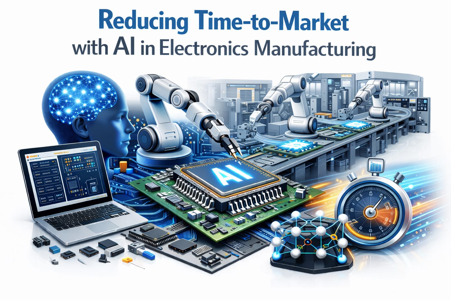
Reducing time-to-market is a critical objective in electronics manufacturing, especially in the highly competitive semiconductor industry where product lifecycles are short and innovation cycles are rapid. Artificial Intelligence (AI) accelerates this process by optimizing design-to-fabrication workflows through predictive analytics and intelligent automation. AI algorithms can forecast manufacturing bottlenecks, predict yield outcomes, and identify potential defects before mass production begins. By analyzing historical fabrication data, process parameters, and equipment performance metrics, machine learning models enable faster process calibration and more accurate production planning. This proactive approach minimizes trial-and-error iterations, shortens validation cycles, and ensures smoother transitions from prototype to high-volume manufacturing.
In addition to yield prediction and defect detection, AI enhances rapid prototyping and supply chain coordination within electronics manufacturing ecosystems. Intelligent scheduling systems optimize production lines by dynamically allocating resources based on demand forecasts and real-time factory data. AI-powered inspection systems using computer vision can detect micro-level defects in wafers and PCBs with higher precision and speed than manual inspection methods. These advancements reduce rework rates, improve production efficiency, and significantly cut down lead times. By embedding AI across manufacturing operations, electronics companies can deliver high-performance products to market faster while maintaining quality, cost efficiency, and competitive advantage.
AI for Power Efficiency and Sustainable Electronics Design

Artificial Intelligence (AI) is playing a pivotal role in improving power efficiency and enabling sustainable electronics design, particularly in advanced semiconductor systems where energy consumption is a primary constraint. As device geometries shrink and transistor density increases, managing dynamic and static power dissipation becomes increasingly complex. AI-driven optimization algorithms analyze switching activity, workload behavior, and architectural configurations to recommend low-power design strategies at the RTL and gate levels. Machine learning models can predict leakage currents, voltage fluctuations, and thermal hotspots early in the design cycle, allowing engineers to implement dynamic voltage and frequency scaling (DVFS), power gating, and clock gating techniques more effectively.
Beyond circuit-level optimization, AI enhances system-level energy management in embedded systems, IoT devices, and high-performance computing platforms. Deep learning models can study real-time usage patterns and adapt hardware resource allocation to minimize unnecessary power consumption. For example, AI-based controllers can intelligently manage processor cores, memory subsystems, and peripheral components based on workload intensity. This adaptive power optimization not only improves battery life in portable electronics but also reduces overall energy demands in data centers and edge computing environments. By integrating predictive analytics into hardware-software co-design, AI ensures that performance targets are met without excessive power overhead.
Sustainable electronics design also benefits from AI-driven lifecycle analysis and green manufacturing practices. Machine learning algorithms assist in selecting energy-efficient materials, optimizing fabrication processes to reduce waste, and improving yield rates to minimize resource consumption. In advanced semiconductor manufacturing, AI-based thermal modeling and energy monitoring systems help reduce carbon footprints while maintaining production efficiency. As environmental regulations and sustainability goals become more stringent, AI emerges as a strategic enabler for designing eco-friendly, power-optimized electronic systems. By combining performance enhancement with responsible energy management, AI supports the development of next-generation electronics that are both technologically advanced and environmentally sustainable.
Real-World Applications of AI in Advanced Electronics

Artificial Intelligence (AI) is driving real-world innovation across multiple domains of advanced electronics, particularly in high-performance and application-specific semiconductor systems. In automotive electronics, AI-enabled chips power Advanced Driver Assistance Systems (ADAS), autonomous driving platforms, and intelligent battery management systems in electric vehicles. These systems rely on AI accelerators and optimized SoCs to process sensor fusion data from LiDAR, radar, and cameras in real time. Similarly, in 5G and next-generation communication infrastructure, AI-optimized RF and baseband processors enhance signal processing efficiency, reduce latency, and improve network reliability. By embedding AI capabilities directly into hardware architectures, manufacturers achieve higher computational throughput while maintaining power efficiency.
AI also plays a significant role in IoT hardware, consumer electronics, and edge computing devices. Smart home controllers, wearable devices, and industrial IoT modules integrate AI-driven microcontrollers capable of on-device inference, reducing dependence on cloud processing and improving response times. In data centers, AI-designed processors and GPUs are optimized for parallel workloads, enabling faster deep learning training and inference operations. Additionally, AI-powered medical electronics—such as diagnostic imaging systems and portable health monitoring devices—leverage intelligent signal processing for accurate real-time analysis. These real-world applications demonstrate how AI is not only optimizing electronics design but also redefining system functionality, performance benchmarks, and industry innovation standards.
Challenges and Limitations of AI in Electronics Design
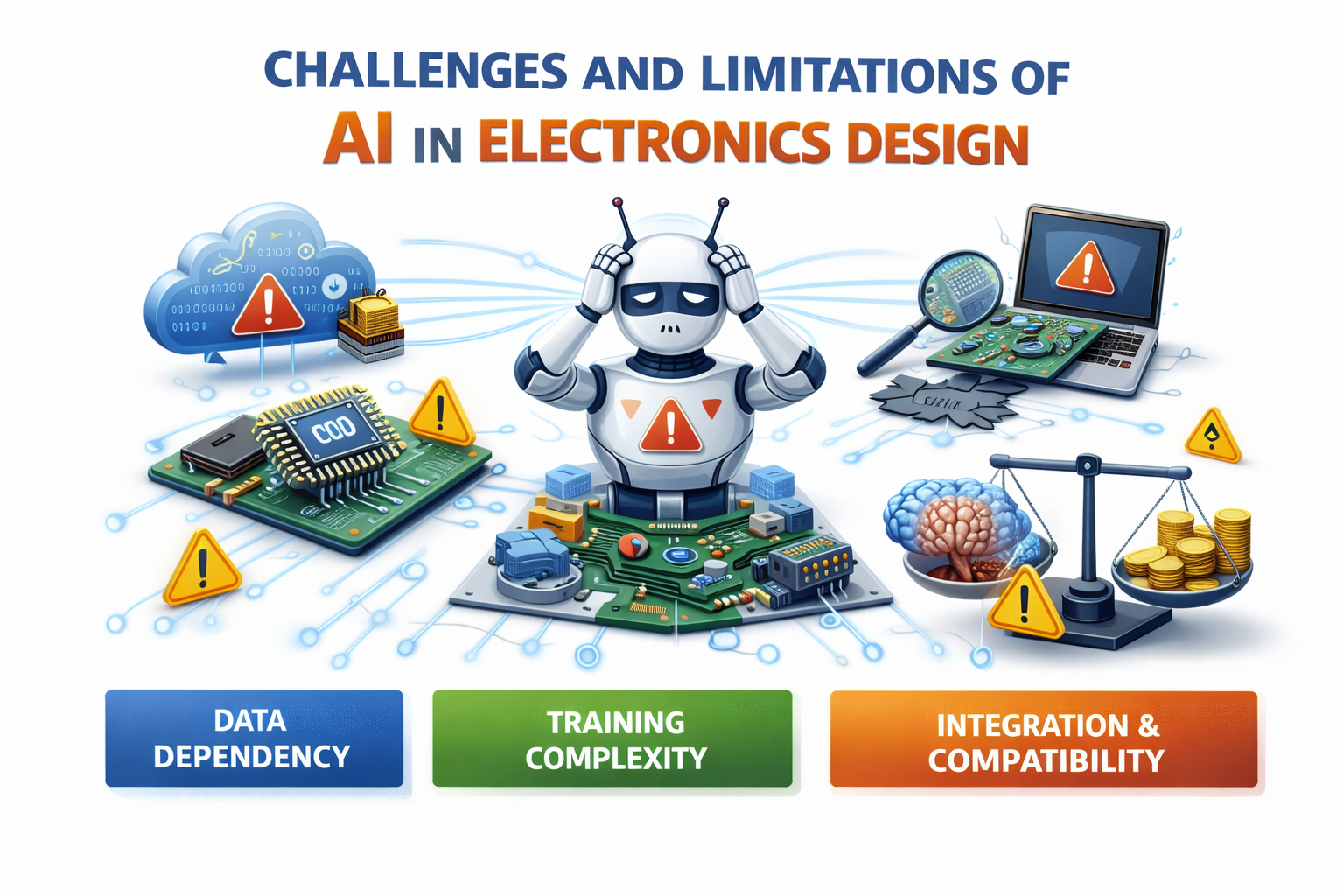
While Artificial Intelligence (AI) is transforming electronics design, it also presents several technical and operational challenges. One major limitation is data dependency. AI and deep learning models require large volumes of high-quality, labeled design and silicon validation data to deliver accurate predictions. In advanced VLSI and semiconductor workflows, such datasets may be proprietary, incomplete, or inconsistent across technology nodes, limiting model generalization. Additionally, training complex neural networks demands substantial computational resources, including high-performance GPUs and large memory capacity, which can increase infrastructure costs. There is also the risk of overfitting, where AI models perform well on historical designs but fail to adapt effectively to new architectures or emerging process technologies.
Another critical challenge lies in integration and interpretability within existing Electronic Design Automation (EDA) environments. Many AI algorithms operate as black-box systems, making it difficult for design engineers to fully understand the reasoning behind optimization decisions. In safety-critical domains such as automotive or aerospace electronics, lack of explainability can hinder adoption due to strict validation and compliance requirements. Furthermore, balancing prediction accuracy with runtime efficiency remains a key trade-off, particularly when AI models are embedded into real-time design flows. To fully realize the benefits of AI in electronics design, organizations must address these limitations through robust data governance, hybrid modeling approaches, and improved explainable AI techniques tailored specifically for semiconductor engineering.
Future Scope of AI and Deep Learning in Semiconductor Industry

The future scope of Artificial Intelligence (AI) and Deep Learning in the semiconductor industry is expansive, with the potential to fundamentally reshape how chips are architected, designed, and manufactured. As technology nodes advance into sub-5nm regimes and chip architectures become increasingly heterogeneous, traditional design methodologies struggle to keep pace with complexity. AI-driven design automation is expected to evolve into fully autonomous optimization systems capable of handling end-to-end chip development—from RTL generation to physical layout and verification. Deep learning models will increasingly support intelligent design space exploration, enabling engineers to evaluate thousands of microarchitectural variations and rapidly converge on optimal Power, Performance, and Area (PPA) targets.
Another major growth area lies in AI-designed and AI-optimized hardware specifically built to accelerate machine learning workloads. Semiconductor companies are investing heavily in domain-specific architectures (DSAs), AI accelerators, neuromorphic chips, and edge AI processors that deliver high computational throughput with minimal power consumption. In addition, AI will play a larger role in advanced packaging technologies such as chiplets and 3D IC integration, where predicting thermal behavior, interconnect latency, and signal integrity becomes more complex. By combining predictive analytics with real-time manufacturing feedback, AI systems will enable adaptive fabrication processes that continuously improve yield and reliability across production cycles.
Looking ahead, the semiconductor industry is likely to transition toward self-learning design ecosystems, where AI models continuously refine themselves based on post-silicon performance data and field deployment feedback. This closed-loop optimization framework will reduce design re-spins, shorten time-to-market, and enhance first-silicon success rates. Moreover, as sustainability becomes a strategic priority, AI will drive energy-efficient chip architectures and environmentally responsible manufacturing practices. With ongoing advancements in machine learning algorithms, computational hardware, and EDA integration, AI and deep learning are set to become foundational pillars of next-generation semiconductor innovation and intelligent electronics development.
Conclusion
Artificial Intelligence and Deep Learning are no longer optional enhancements in advanced electronics design—they are becoming core enablers of innovation across the semiconductor ecosystem. From intelligent RTL optimization and AI-powered EDA tools to predictive verification and smart manufacturing, these technologies are redefining how chips are conceptualized, developed, and delivered. By automating complex design decisions, accelerating simulation cycles, and optimizing Power, Performance, and Area (PPA), AI-driven methodologies significantly reduce time-to-market while improving silicon reliability and efficiency. The integration of data-driven intelligence into VLSI and SoC workflows marks a decisive shift toward smarter, faster, and more scalable electronics engineering practices.
At the same time, the successful adoption of AI in electronics design requires addressing challenges such as data quality, model interpretability, and integration within legacy workflows. As research advances and semiconductor companies continue investing in AI-enabled infrastructure, the industry is moving toward autonomous design ecosystems capable of continuous learning and optimization. Ultimately, AI and Deep Learning will play a strategic role in shaping next-generation semiconductor technologies, enabling sustainable, high-performance, and intelligent electronic systems that meet the growing demands of modern digital applications.