
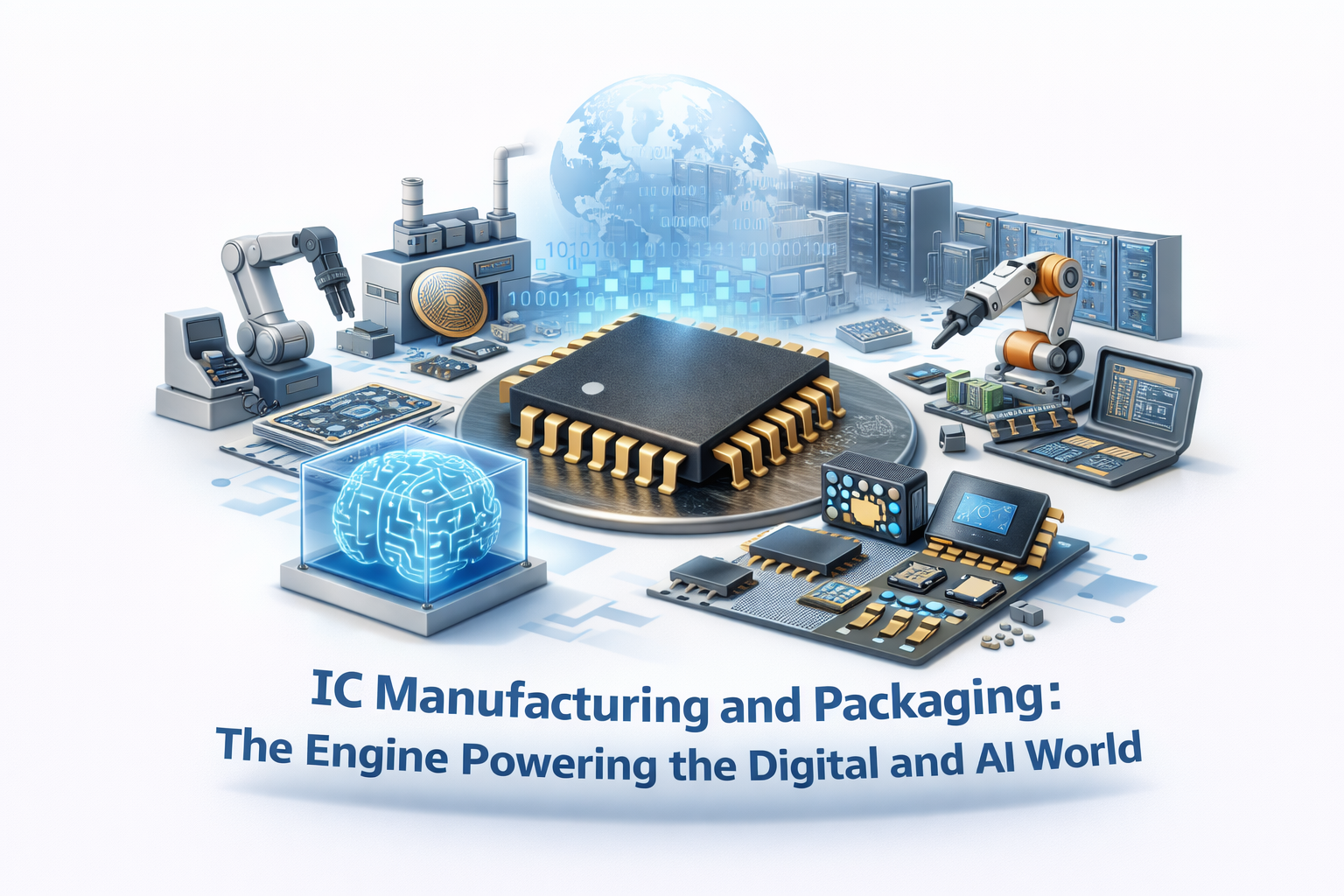
IC Manufacturing and Packaging: The Engine Powering the Digital and AI World
Navigate through this article using the table of contents below
Table of Contents
No headings found in this article.
The digital world we live in today—from smartphones and cloud computing to artificial intelligence and autonomous systems—is powered by one critical technology: integrated circuits (ICs). Behind every powerful processor and intelligent device lies a complex process known as IC manufacturing and semiconductor packaging. These processes transform microscopic electronic designs into physical chips capable of performing billions of operations per second. As industries rapidly adopt AI, 5G, high-performance computing, and IoT technologies, the demand for advanced semiconductor manufacturing and packaging technologies continues to grow, making them the true engine driving the modern digital economy.
IC manufacturing involves a highly sophisticated sequence of steps such as wafer fabrication, photolithography, etching, doping, and testing to create billions of tiny transistors on a silicon wafer. Once fabricated, semiconductor packaging plays a crucial role in protecting the chip, enabling electrical connections, improving thermal performance, and enhancing reliability in real-world applications. Advanced packaging technologies such as 2.5D and 3D packaging, chiplets, and system-in-package (SiP) are becoming essential for modern AI chips and high-performance processors. Together, IC manufacturing and packaging form the backbone of the semiconductor industry, enabling faster, smaller, and more energy-efficient electronic systems that power the digital and AI revolution.
Introduction to IC Manufacturing and Semiconductor Packaging in the AI Era
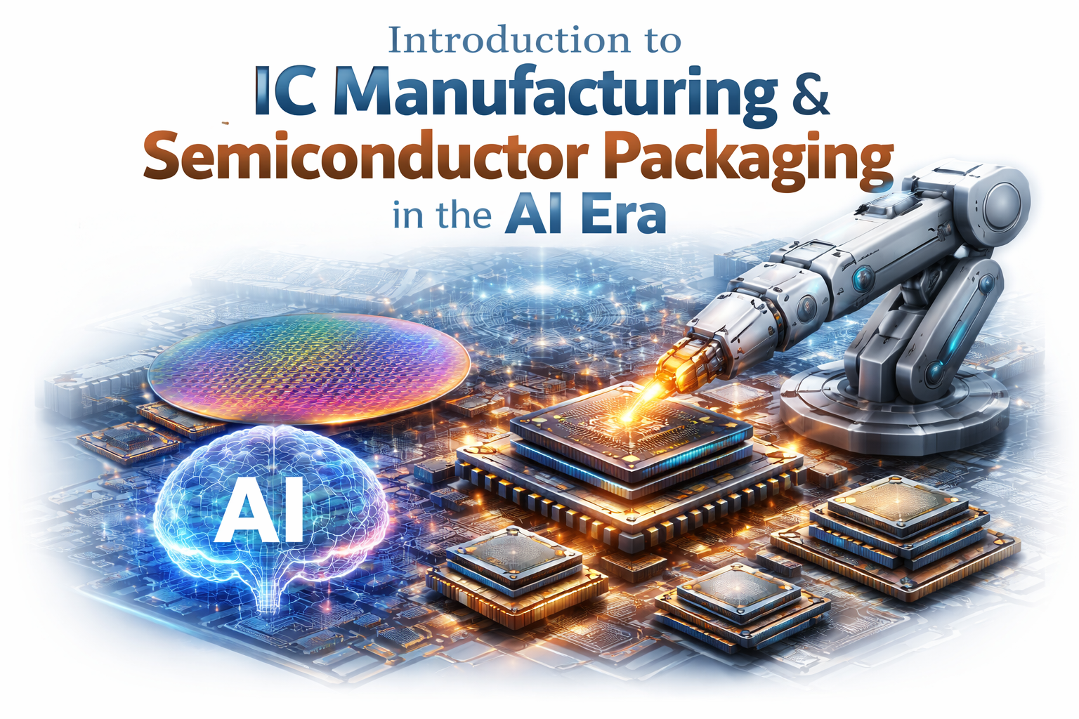
The rapid rise of artificial intelligence, cloud computing, and smart devices has made IC manufacturing and semiconductor packaging more critical than ever before. At the core of every AI-powered system lies a highly sophisticated integrated circuit, designed and fabricated through advanced semiconductor processes. IC manufacturing involves transforming raw silicon into powerful microchips using techniques such as photolithography, etching, deposition, and doping. As AI workloads demand higher performance, lower latency, and improved energy efficiency, modern semiconductor fabrication technologies—especially at advanced nodes like 5nm and 3nm—are evolving rapidly to meet these requirements, making them a cornerstone of the digital transformation era.
Equally important is semiconductor packaging, which goes beyond simply enclosing the chip. Packaging ensures proper electrical connectivity, efficient heat dissipation, and mechanical protection, all of which are crucial for reliable operation in real-world applications. In the AI era, advanced packaging technologies such as 3D ICs, chiplets, and system-in-package (SiP) are enabling higher integration, better performance, and reduced power consumption. Together, IC manufacturing and packaging form a tightly integrated ecosystem that drives innovation across industries, from data centers and autonomous vehicles to consumer electronics, ultimately powering the intelligent systems shaping the future.
Overview of the Semiconductor Manufacturing Process: From Silicon Wafer to Chip
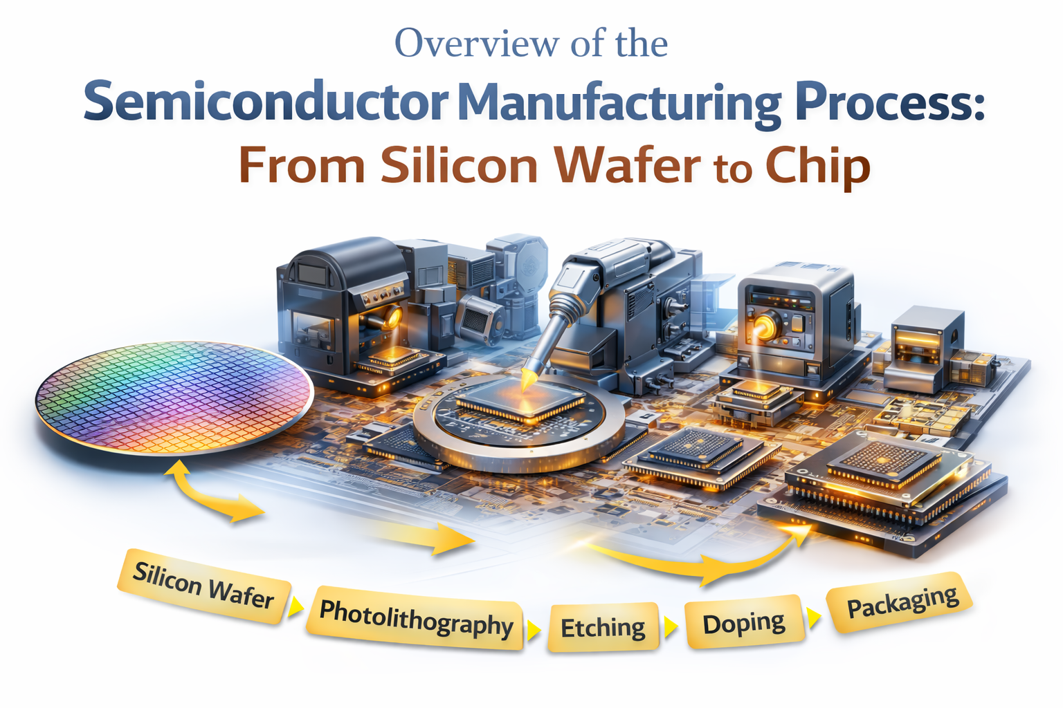
The semiconductor manufacturing process begins with a pure silicon wafer, which serves as the foundation for building integrated circuits. Silicon, derived from sand (silicon dioxide), is refined into a single-crystal structure and sliced into thin wafers with a mirror-like surface. These wafers undergo cleaning and oxidation to prepare them for device fabrication. At this stage, the wafer acts as a blank canvas where billions of transistors will be created, forming the core of modern electronic devices such as processors, memory chips, and AI accelerators.
The next phase involves a series of highly precise fabrication steps, including photolithography, etching, doping, and deposition. Photolithography uses ultraviolet light to transfer intricate circuit patterns onto the wafer, while etching removes unwanted material to define transistor structures. Doping introduces impurities into the silicon to modify its electrical properties, enabling the formation of p-type and n-type regions essential for transistor operation. Deposition techniques, such as chemical vapor deposition (CVD) and physical vapor deposition (PVD), are used to add thin layers of materials, building up complex multi-layered circuit architectures. These steps are repeated multiple times to construct millions or even billions of transistors on a single chip.
Once the wafer fabrication is complete, the process moves to testing, dicing, and packaging. The wafer is tested to identify functional chips, then cut into individual dies. Each die is packaged to protect it from environmental damage and to provide electrical connections to external systems. Advanced packaging techniques also enhance thermal management and performance, especially for high-speed and AI-driven applications. From raw silicon to a fully functional microchip, the semiconductor manufacturing process is a highly controlled and complex workflow that enables the powerful and compact electronics driving today’s digital world.
Key Steps in IC Fabrication: Photolithography, Etching, Doping, and Deposition Explained
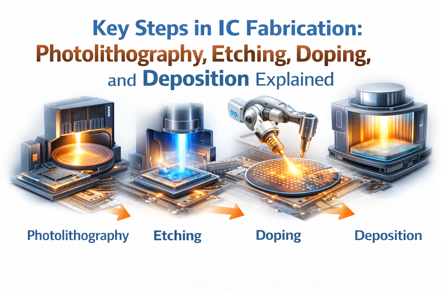
IC fabrication is a highly controlled and repetitive process where multiple patterning and material modification steps are used to build transistors and interconnects on a silicon wafer. One of the most critical steps is photolithography, where ultraviolet (UV) or extreme ultraviolet (EUV) light is used to transfer circuit patterns from a photomask onto a light-sensitive photoresist layer on the wafer. This step defines the geometry of transistors and interconnect layers with nanometer-level precision. Following this, etching is performed to remove unwanted material, either through wet chemical processes or dry plasma etching, creating the physical structures required for device operation.
Another essential step is doping, where controlled amounts of impurities such as boron or phosphorus are introduced into the silicon to modify its electrical properties, forming p-type and n-type regions that are fundamental to transistor functionality. This is typically achieved through ion implantation followed by annealing to activate the dopants. In parallel, deposition processes such as chemical vapor deposition (CVD) and physical vapor deposition (PVD) are used to deposit thin films of materials like silicon dioxide, polysilicon, and metals, which form insulating layers, gate structures, and interconnects. These four key steps—photolithography, etching, doping, and deposition—are repeated multiple times in a precise sequence to build complex, high-performance integrated circuits that power modern electronic and AI-driven systems.
What is Semiconductor Packaging? Types, Techniques, and Importance in Modern Electronics
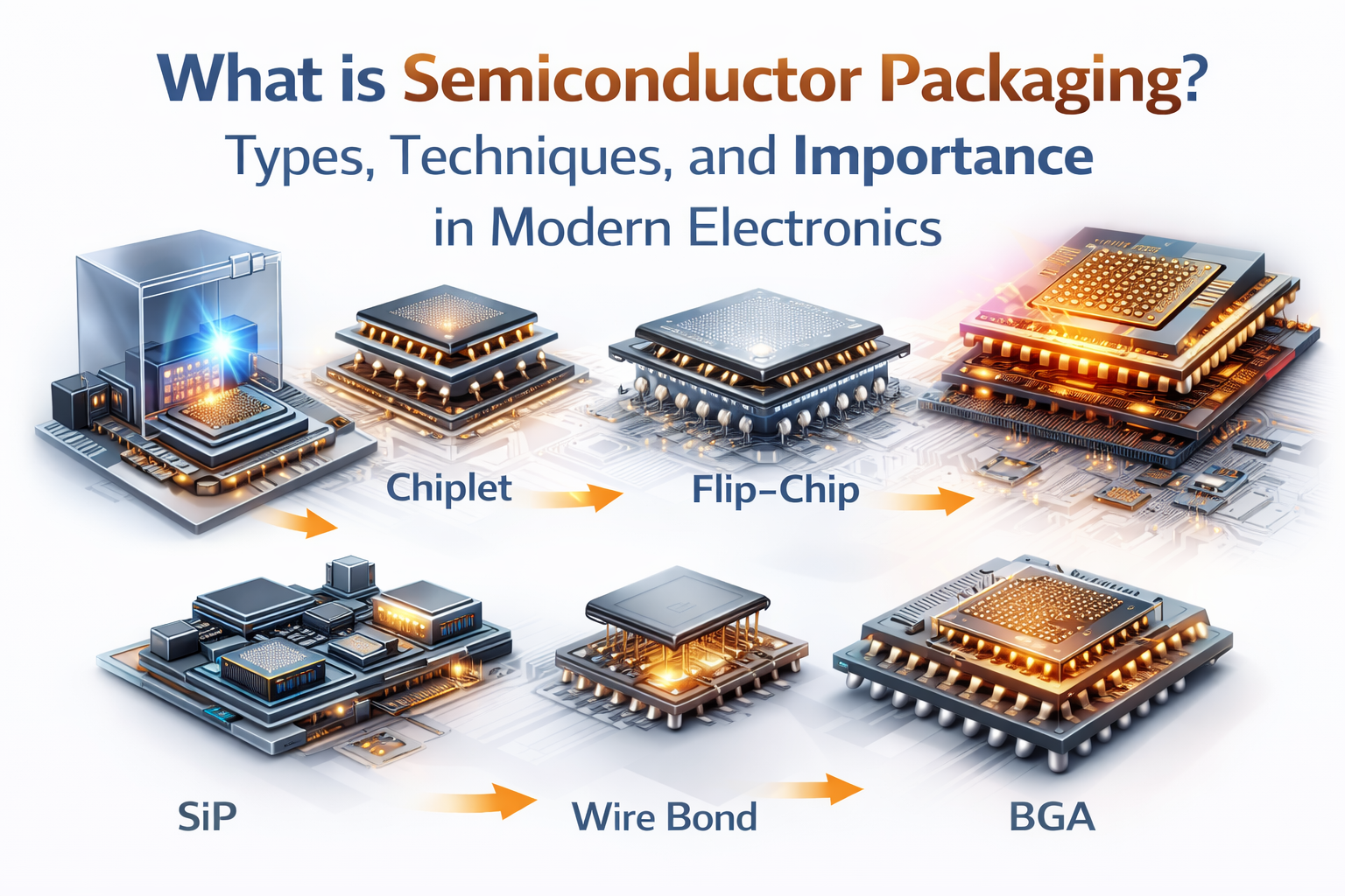
Semiconductor packaging is the final stage of the chip manufacturing process, where a fabricated silicon die is enclosed within a protective structure and connected to the outside world. Its primary purpose is to provide mechanical support, protect the delicate chip from environmental factors such as moisture, heat, and physical damage, and enable electrical connectivity between the chip and the printed circuit board (PCB). Without proper packaging, even the most advanced integrated circuits would be unusable in real-world applications. In modern electronics, packaging has evolved from a simple protective layer to a critical performance enabler that directly impacts speed, power efficiency, and reliability.
There are several types of semiconductor packaging, each designed to meet specific application requirements. Traditional packages include Dual In-line Package (DIP) and Quad Flat Package (QFP), while more advanced solutions include Ball Grid Array (BGA) and Flip-Chip packaging, which offer higher pin density and better electrical performance. Modern techniques such as System-in-Package (SiP) integrate multiple components into a single package, and chiplet-based architectures allow multiple smaller dies to work together as a single system. Additionally, advanced packaging technologies like 2.5D and 3D IC packaging enable vertical stacking of chips, improving performance and reducing interconnect delays, which is especially important for AI and high-performance computing applications.
The importance of semiconductor packaging in modern electronics cannot be overstated, as it directly influences thermal management, signal integrity, and overall system reliability. Efficient heat dissipation mechanisms, such as heat sinks and advanced substrates, are essential for preventing overheating in high-performance chips. Packaging also plays a key role in minimizing signal loss and ensuring high-speed data transmission, which is crucial for applications like 5G, data centers, and autonomous systems. As electronic devices continue to become smaller, faster, and more powerful, semiconductor packaging is emerging as a major innovation driver, bridging the gap between chip design and real-world functionality.
Advanced Packaging Technologies: 2.5D, 3D ICs, Chiplets, and System-in-Package (SiP)
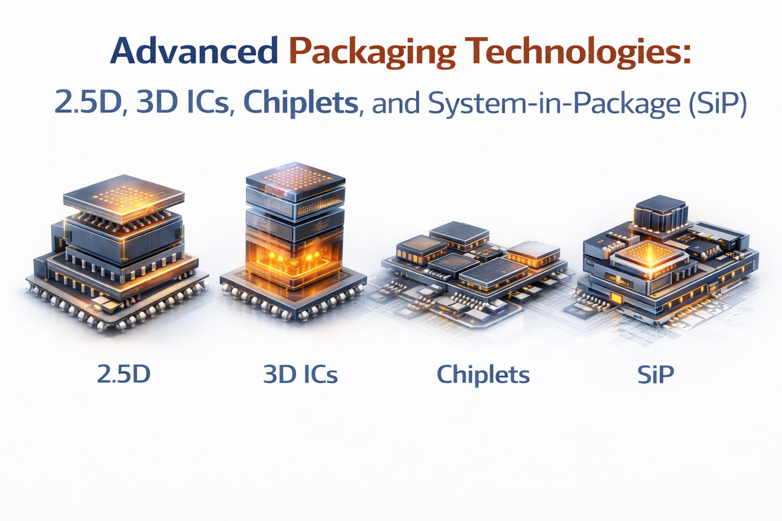
Advanced semiconductor packaging technologies have emerged as a critical solution to overcome the limitations of traditional scaling, especially in the era of AI, high-performance computing, and data-intensive applications. 2.5D packaging uses an interposer (typically silicon or organic) to place multiple dies side-by-side, enabling high-bandwidth communication between chips while maintaining better yield compared to full stacking. In contrast, 3D IC packaging involves vertically stacking multiple dies using technologies like through-silicon vias (TSVs), significantly reducing interconnect length and improving performance, power efficiency, and integration density. These approaches are widely used in advanced processors, GPUs, and memory stacks such as HBM (High Bandwidth Memory).
Another key innovation is the use of chiplet-based architectures, where complex systems are divided into smaller, reusable dies (chiplets) that are interconnected within a single package. This improves design flexibility, reduces manufacturing cost, and allows heterogeneous integration of different process nodes. Similarly, System-in-Package (SiP) integrates multiple components—such as processors, memory, sensors, and passive elements—into a compact package, enabling highly functional and space-efficient electronic systems. Together, these advanced packaging technologies are redefining how modern chips are designed and manufactured, playing a vital role in delivering scalable, high-performance, and energy-efficient solutions for next-generation digital and AI-driven applications.
Role of IC Manufacturing in Powering AI, Machine Learning, and High-Performance Computing
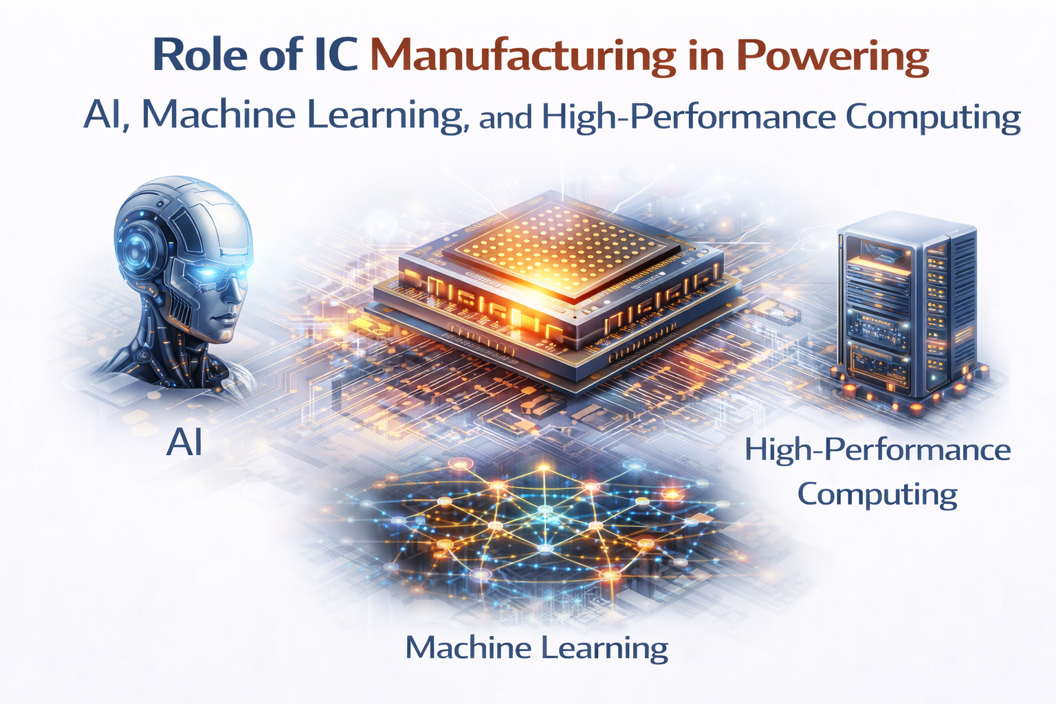
IC manufacturing plays a foundational role in enabling the rapid growth of artificial intelligence (AI), machine learning (ML), and high-performance computing (HPC). These advanced technologies rely on specialized chips—such as GPUs, TPUs, and AI accelerators—that are designed to handle massive parallel computations and data processing workloads. Modern semiconductor manufacturing processes, especially at advanced nodes like 7nm, 5nm, and 3nm, allow for higher transistor density, faster switching speeds, and lower power consumption. This directly translates into improved computational efficiency, making it possible to train complex AI models and run real-time inference in applications such as natural language processing, computer vision, and autonomous systems.
In machine learning and HPC environments, performance is heavily dependent on the ability to process large volumes of data with minimal latency. IC manufacturing innovations such as FinFET and Gate-All-Around (GAA) transistor architectures have significantly enhanced performance while reducing leakage power. Additionally, advanced fabrication techniques enable the integration of high-bandwidth memory (HBM) and specialized interconnects, which are critical for data-intensive workloads. These manufacturing advancements ensure that processors can handle complex algorithms, deep neural networks, and large-scale simulations efficiently, supporting industries ranging from healthcare and finance to automotive and cloud computing.
Furthermore, IC manufacturing is closely linked with advanced packaging technologies, which together enable the next generation of AI and HPC systems. Techniques like 2.5D and 3D integration, along with chiplet-based designs, allow multiple processing units and memory components to be combined within a single package, improving data transfer speeds and overall system performance. As AI models continue to grow in complexity and computational demand, the role of semiconductor manufacturing becomes even more critical. It not only drives innovation in chip design but also ensures scalability, energy efficiency, and reliability, making it the backbone of the digital and AI-powered world.
Importance of Thermal Management and Reliability in IC Packaging
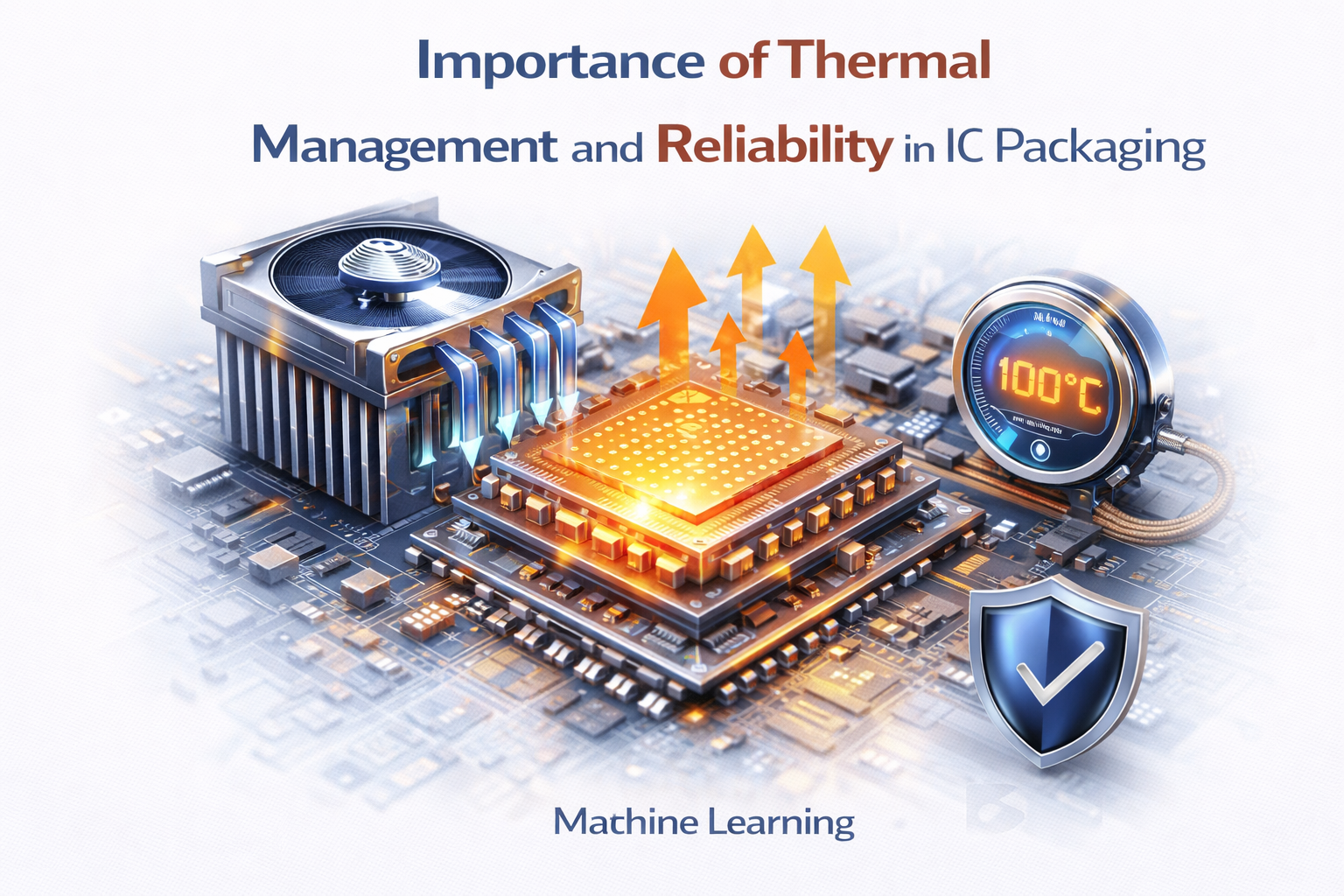
Thermal management is a critical aspect of IC packaging, as modern semiconductor devices generate significant heat due to high transistor density and increased power consumption. Without efficient heat dissipation, excessive temperatures can degrade performance, cause timing failures, and even lead to permanent damage of the chip. IC packaging incorporates various thermal solutions such as heat sinks, thermal interface materials (TIMs), heat spreaders, and advanced substrates to efficiently transfer heat away from the silicon die. In high-performance applications like AI processors, GPUs, and data center chips, effective thermal management is essential to maintain stable operation, prevent thermal throttling, and ensure optimal system performance.
Reliability in IC packaging is equally important, as packaged chips must withstand mechanical stress, temperature variations, and long-term operational wear. Factors such as electromigration, thermal cycling, and material fatigue can impact the lifespan and functionality of semiconductor devices. Advanced packaging techniques are designed to improve reliability by enhancing structural integrity, minimizing signal degradation, and ensuring consistent electrical connections over time. As electronic systems become more compact and powerful, maintaining both thermal efficiency and reliability is crucial for delivering durable, high-performance products across industries such as automotive, telecommunications, healthcare, and consumer electronics.
Challenges in Modern Semiconductor Manufacturing at Advanced Technology Nodes (5nm, 3nm, and Beyond)
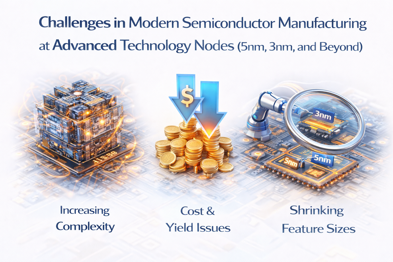
As semiconductor technology advances into 5nm, 3nm, and beyond, manufacturing complexity has increased exponentially, making chip fabrication more challenging than ever. One of the primary challenges is the limitation of traditional scaling, as shrinking transistor dimensions leads to quantum effects such as leakage current and variability. Advanced lithography techniques like Extreme Ultraviolet (EUV) are required to pattern these tiny features, but they come with high equipment costs, process complexity, and stringent defect control requirements. Maintaining precision at the atomic scale while ensuring consistent performance across billions of transistors is a major engineering hurdle in modern semiconductor manufacturing.
Another significant challenge is the rising cost and declining yield associated with advanced nodes. Fabrication facilities (fabs) for 5nm and 3nm technologies require multi-billion-dollar investments, making them accessible only to a few leading semiconductor companies. At these nodes, even minor defects can render chips non-functional, reducing yield and increasing production costs. Additionally, process variations and reliability concerns—such as electromigration, gate oxide breakdown, and thermal effects—become more pronounced, requiring advanced design-for-manufacturability (DFM) techniques and robust testing methodologies to ensure acceptable product quality.
Power consumption and heat dissipation also present major obstacles at advanced technology nodes. As transistor density increases, managing power efficiency while maintaining high performance becomes increasingly difficult. This has led to the adoption of new transistor architectures such as FinFET and Gate-All-Around (GAA) to improve control over current flow and reduce leakage. Furthermore, integration challenges, including interconnect scaling and signal integrity, require innovations in materials and packaging technologies. Addressing these challenges is critical for sustaining the progress of Moore’s Law and enabling next-generation applications in AI, high-performance computing, and advanced digital systems.
Career Opportunities in IC Manufacturing and Semiconductor Packaging Engineering
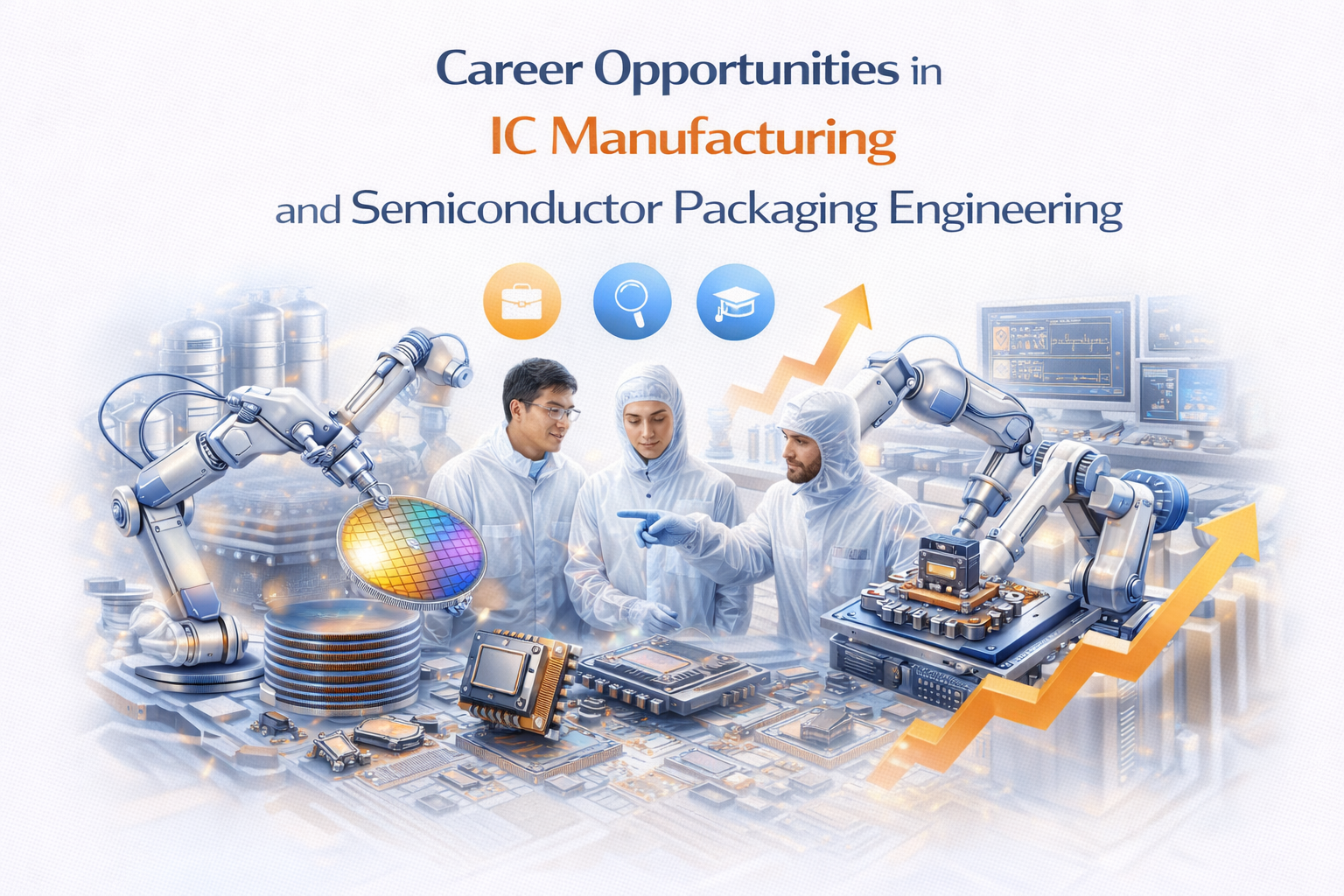
Career opportunities in IC manufacturing and semiconductor packaging engineering are expanding rapidly due to the global demand for advanced chips powering AI, 5G, automotive electronics, and high-performance computing. In IC manufacturing, professionals typically work in roles such as process engineer, equipment engineer, yield engineer, and fabrication (fab) engineer, where they focus on optimizing wafer fabrication processes, improving yield, and maintaining high-precision production environments. On the packaging side, roles like packaging engineer, reliability engineer, and thermal engineer are critical for designing efficient chip packaging solutions that ensure performance, durability, and heat management. These roles require strong knowledge of semiconductor physics, materials science, and hands-on experience with fabrication and testing tools.
With countries like India investing heavily in semiconductor ecosystems, career prospects in this domain are becoming increasingly attractive for electronics and VLSI graduates. Entry-level engineers often start with roles in process integration, testing, or quality control and can progress to senior positions such as process development engineer, packaging architect, or technology lead. Additionally, expertise in advanced packaging technologies like chiplets, 3D ICs, and system-in-package (SiP) can significantly boost career growth and salary potential. As the semiconductor industry continues to evolve, professionals in IC manufacturing and packaging will play a vital role in enabling next-generation technologies, making this field a promising and future-proof career path.
Future Scope of IC Manufacturing and Packaging in the Digital and AI-Driven World
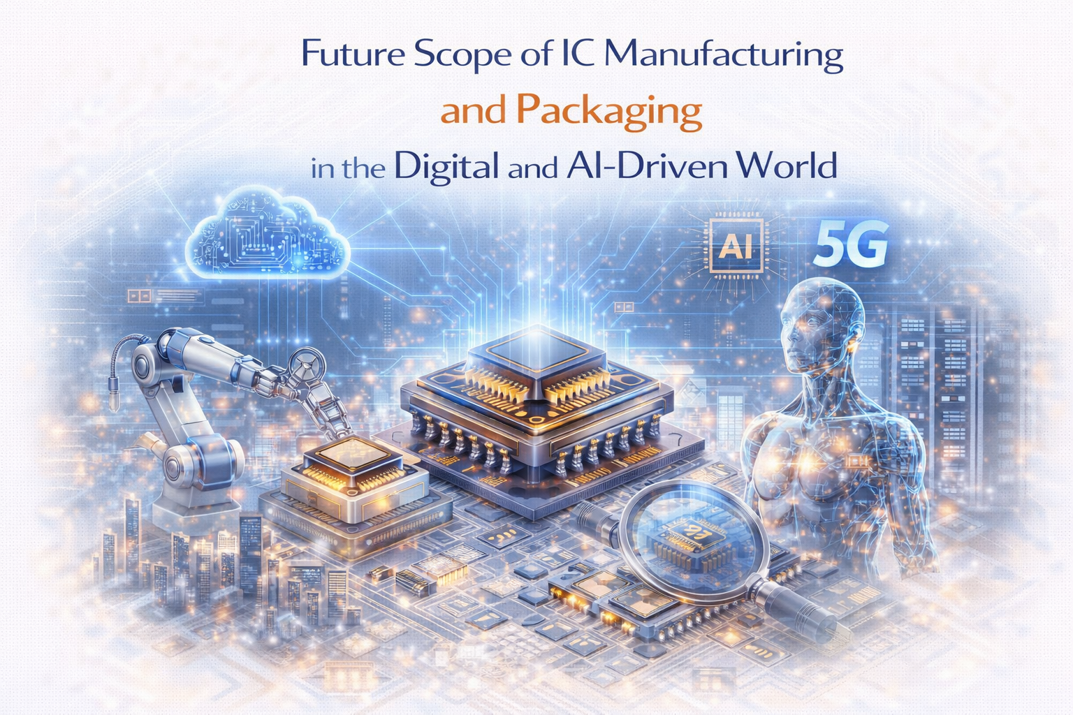
The future of IC manufacturing and semiconductor packaging is closely tied to the rapid expansion of artificial intelligence (AI), edge computing, 5G/6G communication, and high-performance computing systems. As digital technologies become more data-intensive and compute-heavy, there is a growing need for chips that deliver higher performance with lower power consumption. Advanced semiconductor nodes such as 3nm and beyond, along with emerging transistor architectures like Gate-All-Around (GAA), are expected to drive the next wave of innovation. At the same time, the industry is moving beyond traditional Moore’s Law scaling, focusing on system-level integration and co-optimization of design, manufacturing, and packaging to meet future demands.
Semiconductor packaging is set to play an even more critical role in this evolution, particularly with the rise of heterogeneous integration. Technologies such as 2.5D and 3D ICs, chiplets, and system-in-package (SiP) will enable multiple functional components—logic, memory, and accelerators—to be integrated into a single compact package. This approach not only improves performance and bandwidth but also reduces latency and power consumption, which are essential for AI workloads and real-time data processing. Additionally, innovations in advanced materials, thermal solutions, and interconnect technologies will further enhance the efficiency and reliability of next-generation semiconductor systems.
Looking ahead, the global push for semiconductor self-reliance and supply chain resilience—especially in regions like India, the US, and Europe—will create massive opportunities for growth in IC manufacturing and packaging. Government initiatives, investments in fabrication facilities, and increasing demand for indigenous chip design are expected to boost job creation and technological advancements. As industries such as autonomous vehicles, smart cities, healthcare, and IoT continue to expand, IC manufacturing and packaging will remain at the core of innovation, making them indispensable to the future of the digital and AI-driven world.
Conclusion
IC manufacturing and semiconductor packaging form the backbone of today’s digital and AI-driven ecosystem, enabling everything from smartphones and cloud computing to advanced machine learning and high-performance computing systems. As discussed throughout this blog, the journey from raw silicon to a fully functional chip involves highly complex processes, cutting-edge technologies, and continuous innovation. From fabrication techniques like photolithography and doping to advanced packaging solutions such as 3D ICs and chiplets, every stage plays a crucial role in delivering performance, efficiency, and reliability in modern electronic systems.
Looking ahead, the importance of IC manufacturing and packaging will only continue to grow as industries demand faster, smaller, and more power-efficient devices. With emerging trends like heterogeneous integration, advanced nodes, and AI-specific chip architectures, the semiconductor industry is entering a new era of innovation. For aspiring engineers and professionals, this field offers immense career opportunities and long-term growth potential. Ultimately, IC manufacturing and packaging are not just supporting technologies—they are the true engine powering the future of the digital and AI world.