

Semiconductor Design for Electric Vehicles: A Complete Guide of 2026
Navigate through this article using the table of contents below
Table of Contents
No headings found in this article.
The future of mobility is being rewritten at the silicon level. As electric vehicles (EVs) rapidly replace internal combustion engine cars, semiconductor design for electric vehicles has emerged as the backbone of performance, safety, and efficiency. From high-power traction inverters to intelligent battery management systems (BMS) and advanced driver assistance systems (ADAS), modern EVs rely on cutting-edge automotive semiconductor technologies. In 2026, innovations in power electronics, AI-enabled automotive chips, and wide-bandgap materials like SiC and GaN are transforming how electric vehicles are designed, optimized, and manufactured.
This complete guide explores the core aspects of semiconductor design in EVs, including power management ICs, microcontrollers (MCUs), automotive SoCs, sensor integration, thermal design challenges, and functional safety standards such as ISO 26262. Whether you are an electronics engineer, VLSI professional, automotive enthusiast, or student aiming to enter the semiconductor industry, this guide provides a structured and practical overview of EV chip architecture, design methodologies, and future trends shaping the electric mobility ecosystem in 2026 and beyond.
Introduction to Semiconductor Design in Electric Vehicles
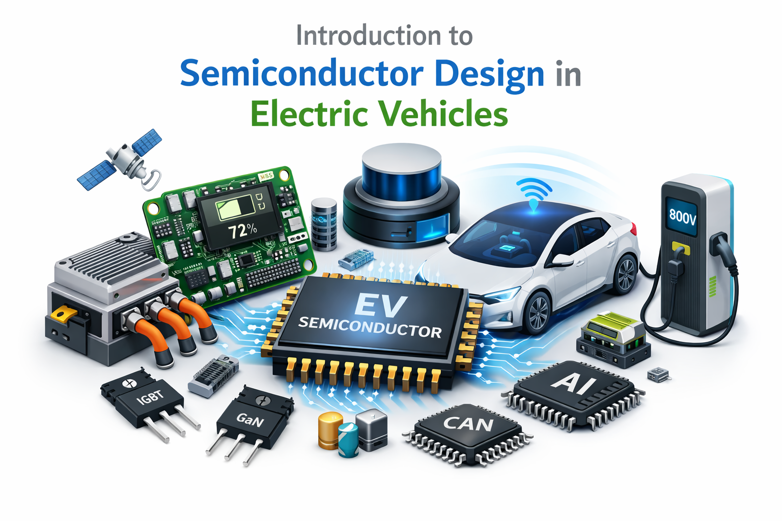
The rapid acceleration of electric mobility has fundamentally transformed automotive engineering, placing semiconductor design in electric vehicles (EVs) at the core of innovation. Unlike traditional internal combustion engine vehicles, EVs depend almost entirely on advanced semiconductor components to manage power conversion, energy storage, motor control, and real-time decision-making systems. From traction inverters and battery management systems (BMS) to onboard chargers and vehicle control units, automotive-grade chips serve as the digital and electrical backbone of modern electric vehicles. As global EV adoption rises in 2026, demand for high-performance, energy-efficient, and safety-compliant semiconductor solutions continues to grow exponentially.
Semiconductor design for EVs differs significantly from consumer electronics due to stringent automotive requirements such as high reliability, extended temperature tolerance, functional safety compliance (ISO 26262), and long lifecycle support. Power semiconductors like IGBTs, MOSFETs, and increasingly Silicon Carbide (SiC) devices are engineered to handle high voltages and currents with minimal switching losses, improving overall vehicle efficiency and driving range. In parallel, automotive microcontrollers (MCUs) and system-on-chips (SoCs) integrate advanced processing capabilities to support regenerative braking systems, torque vector control, and real-time diagnostics. These specialized semiconductor architectures ensure optimal performance while maintaining safety and durability under harsh operating conditions.
In 2026, the evolution of EV semiconductor technology is closely tied to advancements in wide-bandgap materials, AI-enabled automotive chips, and software-defined vehicle architectures. Manufacturers are shifting toward centralized domain controllers and high-performance computing platforms that consolidate multiple electronic control units (ECUs) into fewer, more powerful chips. This transition not only reduces system complexity but also enhances scalability and over-the-air (OTA) update capabilities. As a result, semiconductor design has become a strategic differentiator in the electric vehicle ecosystem, influencing battery efficiency, charging speed, autonomous driving capabilities, and the overall user experience.
Role of Power Electronics in EV Semiconductor Design
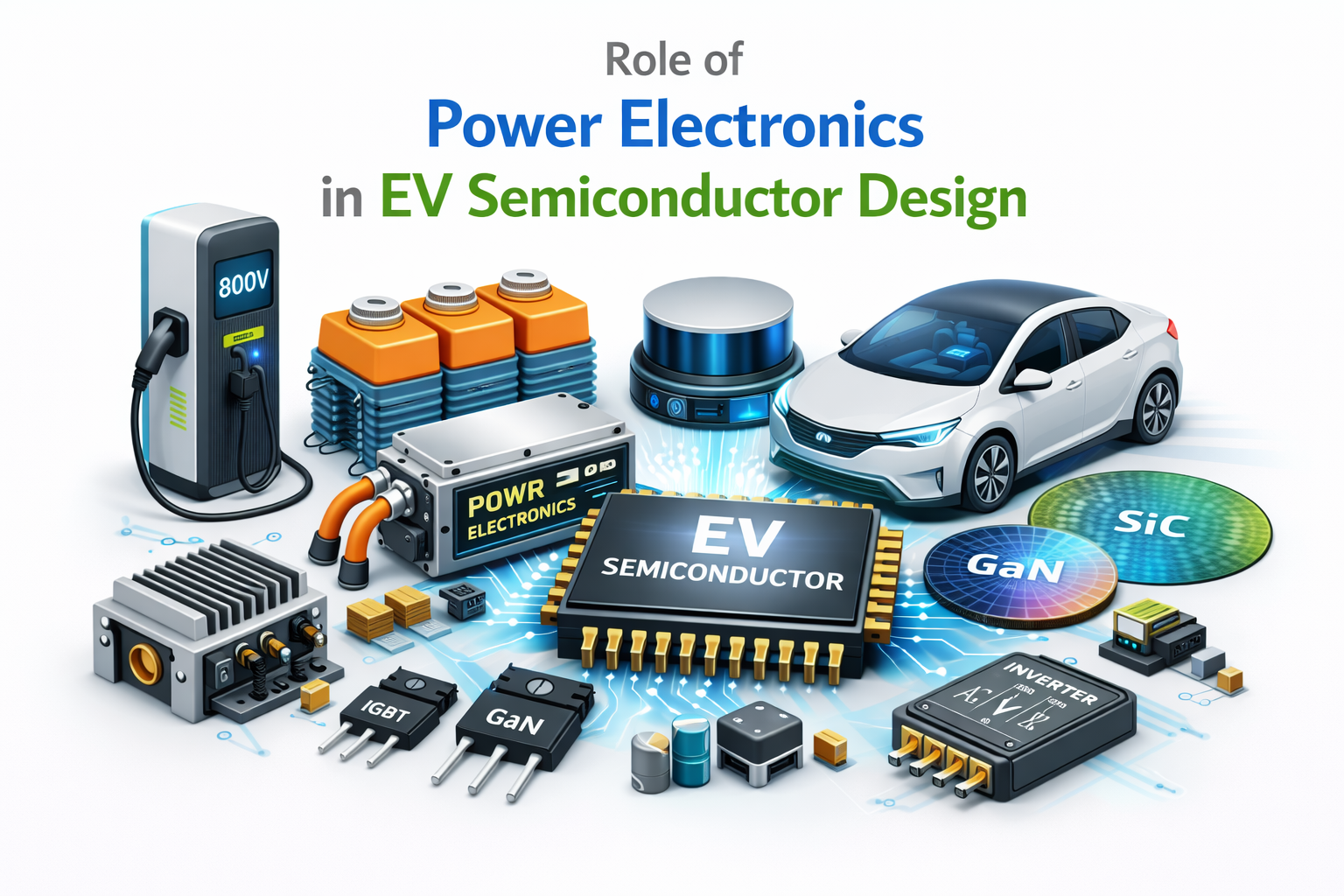
Power electronics form the foundation of EV semiconductor design, as they control the conversion, regulation, and distribution of electrical energy within an electric vehicle. The most critical component is the traction inverter, which converts DC power from the battery into AC power to drive the electric motor with high efficiency and precise torque control. In addition, DC-DC converters regulate voltage levels for auxiliary systems, while onboard chargers manage AC-to-DC conversion during vehicle charging. These systems rely on high-performance power semiconductors such as IGBTs, MOSFETs, and increasingly Silicon Carbide (SiC) devices to handle high voltages and switching frequencies with minimal energy loss, directly impacting vehicle range and performance.
Advanced power semiconductor design in EVs focuses on reducing switching losses, improving thermal efficiency, and ensuring automotive-grade reliability under extreme operating conditions. Wide-bandgap materials like SiC and GaN enable higher efficiency, faster switching speeds, and compact power module designs, which contribute to lighter and more energy-efficient vehicles. Engineers must also address electromagnetic interference (EMI), heat dissipation, and long-term durability to meet strict automotive standards such as ISO 26262. As EV architectures evolve toward 800V platforms and ultra-fast charging systems in 2026, power electronics semiconductor innovation remains central to achieving higher efficiency, improved battery performance, and enhanced overall vehicle reliability.
Battery Management System (BMS) IC Design for EVs
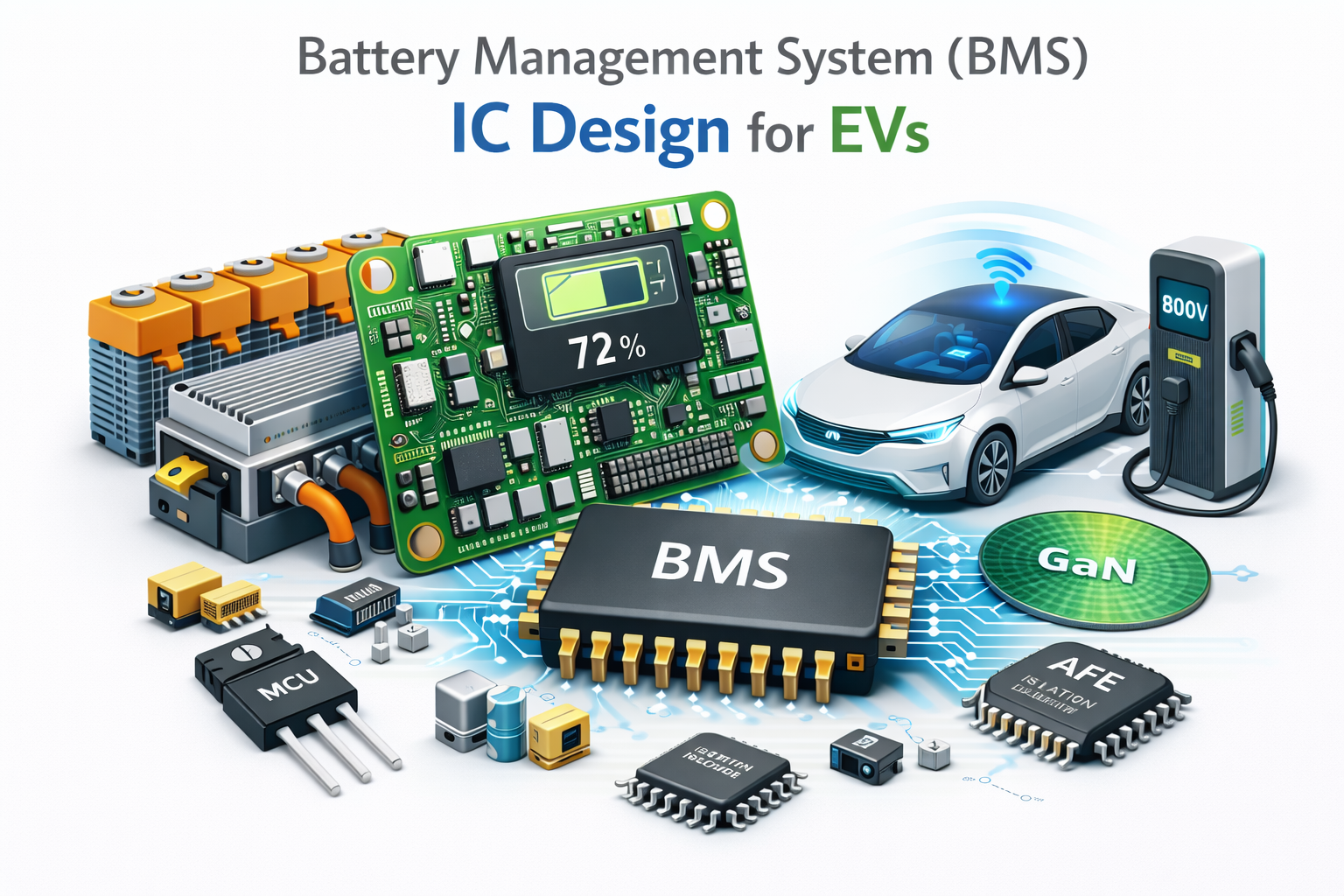
A Battery Management System (BMS) IC is one of the most critical semiconductor components in an electric vehicle, responsible for ensuring battery safety, efficiency, and longevity. In EV semiconductor design, BMS integrated circuits continuously monitor key parameters such as cell voltage, current, temperature, and state of charge (SoC). Since an EV battery pack consists of hundreds or even thousands of lithium-ion cells connected in series and parallel configurations, precise cell-level monitoring is essential to prevent overcharging, deep discharge, and thermal runaway. Advanced BMS ICs incorporate high-accuracy analog front ends (AFEs), data acquisition systems, and embedded microcontrollers to enable real-time diagnostics and predictive battery health analysis.
Modern BMS semiconductor design also focuses heavily on cell balancing techniques and functional safety compliance. Passive and active balancing circuits ensure uniform charge distribution across cells, which improves battery performance and extends lifecycle. Automotive-grade BMS ICs are engineered to meet stringent standards such as ISO 26262, incorporating built-in redundancy, fault detection mechanisms, and self-diagnostic features to maintain safe operation under extreme temperature and load conditions. High-voltage isolation, low-power consumption modes, and robust communication interfaces such as CAN and SPI are also integrated to support reliable system-level integration within the EV architecture.
In 2026, advancements in BMS IC design are increasingly driven by AI-based algorithms and next-generation battery chemistries. Intelligent battery management systems now leverage machine learning models to predict state of health (SoH), optimize charging cycles, and enhance fast-charging performance without compromising safety. Additionally, the shift toward 800V EV platforms and solid-state batteries demands higher precision measurement circuits and improved thermal management strategies. As electric vehicles become more software-defined and energy-dense, BMS semiconductor innovation remains a key enabler of extended driving range, faster charging infrastructure compatibility, and long-term battery reliability.
ADAS and Autonomous Driving Chip Design

ADAS (Advanced Driver Assistance Systems) and autonomous driving chip design represent one of the most performance-intensive domains within EV semiconductor architecture. These automotive chips process massive volumes of real-time data from cameras, LiDAR, radar, ultrasonic sensors, and vehicle dynamics modules to enable features such as adaptive cruise control, lane-keeping assist, automatic emergency braking, and self-parking. High-performance automotive SoCs integrate CPUs, GPUs, AI accelerators, and neural processing units (NPUs) to execute complex perception, sensor fusion, and decision-making algorithms with ultra-low latency. The semiconductor design challenge lies in balancing computational throughput (TOPS), power efficiency, and deterministic real-time performance while meeting automotive-grade reliability standards.
From a design perspective, autonomous driving semiconductor development requires functional safety compliance (ISO 26262 ASIL-D), hardware redundancy, fail-operational architectures, and robust cybersecurity integration. Advanced packaging technologies, high-bandwidth memory interfaces, and automotive Ethernet connectivity are essential to support centralized domain controllers and software-defined vehicle platforms in 2026. Thermal management is also critical, as ADAS processors operate under high workloads in constrained automotive environments. As EVs transition toward higher autonomy levels, chip designers are focusing on scalable AI architectures, over-the-air (OTA) update capability, and edge AI optimization, making ADAS semiconductor innovation a defining factor in next-generation electric mobility systems.
VLSI Design Flow for Automotive Semiconductor Development
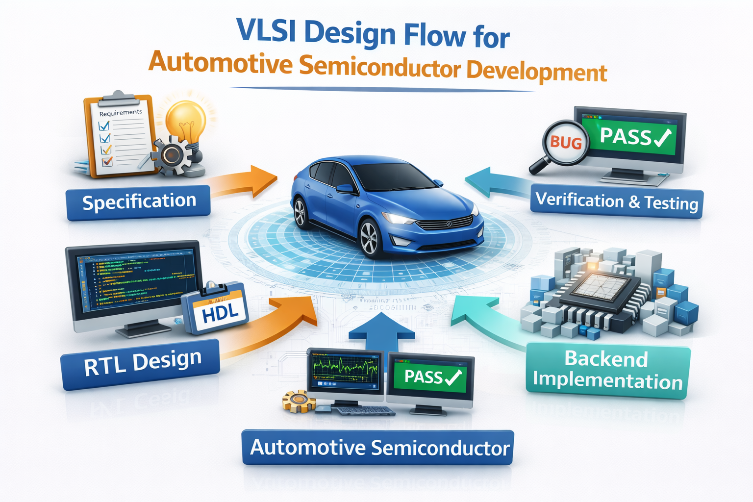
The VLSI design flow for automotive semiconductor development follows a structured, verification-driven methodology to ensure high reliability, functional safety, and long lifecycle support required in electric vehicles. The process begins with system specification and architecture definition, where power, performance, and safety requirements (including ISO 26262 ASIL levels) are defined. This is followed by RTL design using hardware description languages such as Verilog or VHDL, where the functional behavior of automotive SoCs, MCUs, or power management ICs is modeled. Rigorous functional verification—using simulation, constrained random verification, formal verification, and UVM-based environments—is critical at this stage to ensure coverage closure and eliminate design bugs before synthesis. The RTL is then synthesized into gate-level netlists, optimized for timing, power, and area (PPA), and prepared for physical implementation.
During the physical design phase, engineers perform floorplanning, placement, clock tree synthesis (CTS), routing, and signoff checks including static timing analysis (STA), signal integrity, IR drop, and electromigration analysis. Automotive semiconductor development requires additional reliability validation such as fault injection testing, design-for-test (DFT) insertion, and compliance with AEC-Q100 qualification standards. Post-silicon validation further ensures the chip operates correctly under extreme temperature ranges and high-voltage conditions typical in EV environments. In 2026, advanced nodes, chiplet architectures, and AI-assisted EDA tools are increasingly integrated into the automotive VLSI workflow, enabling scalable, high-performance, and safety-compliant semiconductor solutions for next-generation electric vehicles.
Automotive Communication Protocols and Networking ICs
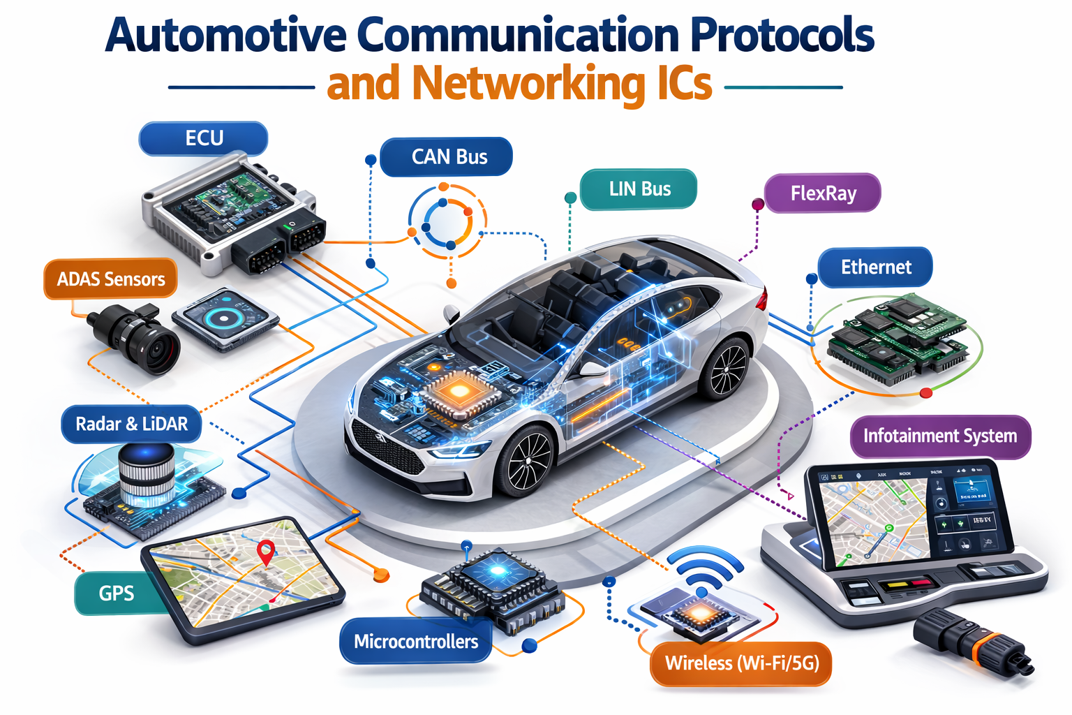
Automotive communication protocols and networking ICs are essential for enabling reliable data exchange between electronic control units (ECUs) in modern electric vehicles. As EV architectures evolve toward software-defined and centralized domain controller models, the need for high-speed, low-latency, and fault-tolerant communication networks has become critical. Traditional protocols such as Controller Area Network (CAN) and Local Interconnect Network (LIN) are widely used for body electronics and low-speed control applications, while more advanced systems like FlexRay and Automotive Ethernet support higher bandwidth requirements for powertrain control, ADAS, and infotainment systems. Networking ICs designed for these protocols ensure deterministic communication, error detection, and robust performance under harsh automotive conditions.
From a semiconductor design perspective, automotive networking ICs must meet stringent requirements for electromagnetic compatibility (EMC), temperature tolerance, and functional safety compliance (ISO 26262). These integrated circuits include transceivers, network controllers, and gateway processors that manage data routing between multiple in-vehicle networks. With the growing complexity of EV systems, secure communication has become a primary design focus. Modern automotive communication chips integrate hardware-based encryption, secure boot mechanisms, and intrusion detection support to protect against cyber threats, particularly as vehicles increasingly rely on over-the-air (OTA) software updates and cloud connectivity.
In 2026, Automotive Ethernet is emerging as the backbone of next-generation EV networking due to its scalability and high data throughput, supporting advanced driver assistance systems and autonomous driving platforms. Time-Sensitive Networking (TSN) capabilities further enhance real-time data synchronization across distributed vehicle systems. Additionally, zonal architectures are reducing wiring complexity by consolidating communication nodes, increasing the demand for high-performance gateway ICs. As electric vehicles become more connected and data-driven, semiconductor innovation in automotive networking remains fundamental to ensuring performance, safety, cybersecurity, and system-level integration.
EV Charging Infrastructure Semiconductor Requirements
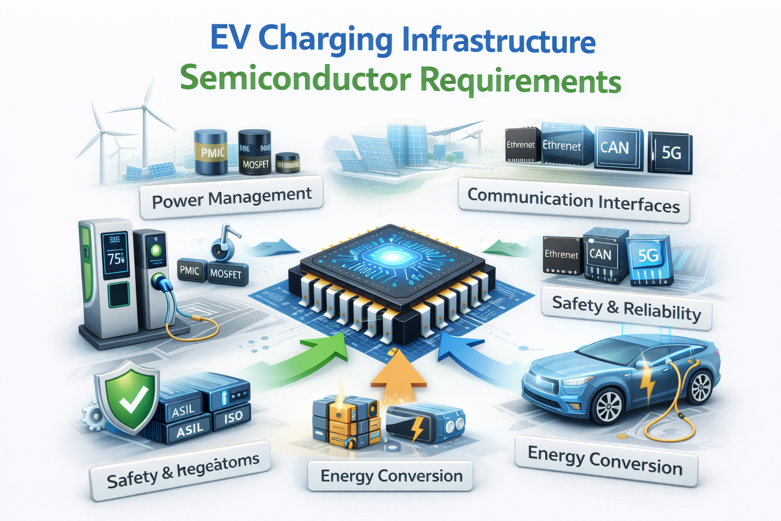
EV charging infrastructure semiconductor requirements are centered on high-efficiency power conversion, fast-switching capability, and grid-level reliability. Fast chargers—especially DC fast-charging systems—depend on advanced power semiconductors such as IGBTs, Silicon MOSFETs, and increasingly Silicon Carbide (SiC) and Gallium Nitride (GaN) devices to handle high voltages and currents with minimal switching losses. These components are used in AC-DC rectification, DC-DC conversion stages, and power factor correction (PFC) circuits to ensure maximum energy transfer efficiency and reduced thermal stress. As charging stations move toward ultra-fast 350 kW and 800V architectures in 2026, semiconductor devices must support higher switching frequencies, improved thermal conductivity, and compact power module integration to reduce system size and energy loss.
Beyond power devices, EV charging infrastructure also requires specialized control ICs, microcontrollers, isolation components, and secure communication chips. Smart charging systems integrate metering ICs, grid-monitoring semiconductors, and communication protocols such as PLC and Ethernet to enable real-time energy management and load balancing. Cybersecurity-enabled semiconductor solutions are critical to protect against grid vulnerabilities, especially in bidirectional charging applications like Vehicle-to-Grid (V2G). Additionally, robust semiconductor design must ensure compliance with safety standards, electromagnetic compatibility (EMC) requirements, and long operational lifecycles, making advanced semiconductor innovation a cornerstone of reliable, scalable EV charging networks.
Semiconductor Supply Chain and Manufacturing Trends in 2026

The semiconductor supply chain and manufacturing landscape in 2026 is undergoing structural transformation driven by rising demand from electric vehicles, AI computing, and advanced automotive electronics. EV semiconductor design increasingly depends on mature nodes such as 28nm, 40nm, and 65nm for power management ICs and microcontrollers, while high-performance ADAS and autonomous driving SoCs leverage advanced nodes like 7nm and below. Foundries are expanding automotive-grade production capacity with enhanced quality control, extended product lifecycles, and AEC-Q100 qualification processes. Additionally, geopolitical factors and lessons from recent chip shortages have accelerated regional manufacturing investments, promoting supply chain diversification and localized fabrication ecosystems to reduce dependency risks.
Manufacturing trends in 2026 also highlight the growing adoption of wide-bandgap semiconductor fabrication, particularly Silicon Carbide (SiC) wafer production, to meet EV power electronics demand. Advanced packaging technologies—such as chiplets, system-in-package (SiP), and 3D integration—are becoming mainstream to improve performance, thermal efficiency, and scalability without solely relying on node shrinkage. Automotive OEMs are increasingly collaborating directly with semiconductor companies to secure long-term supply agreements and co-develop custom chips for software-defined vehicles. As EV production scales globally, supply chain resilience, wafer capacity expansion, and innovation in semiconductor manufacturing processes remain critical to sustaining growth in the automotive electronics sector.
Future Trends in EV Semiconductor Design

The future of EV semiconductor design is being shaped by the rapid transition toward software-defined vehicles (SDVs), where centralized computing platforms replace distributed electronic control units (ECUs). In 2026 and beyond, high-performance automotive SoCs integrate multiple domains—powertrain control, ADAS, infotainment, and connectivity—into scalable chip architectures. This consolidation reduces system complexity, wiring weight, and latency while enabling over-the-air (OTA) software updates and feature upgrades. As a result, semiconductor designers are prioritizing heterogeneous computing architectures that combine CPUs, GPUs, NPUs, and dedicated accelerators to support real-time AI workloads with optimized power efficiency.
Another major trend is the expansion of wide-bandgap semiconductor technologies such as Silicon Carbide (SiC) and Gallium Nitride (GaN), particularly in EV power electronics. These materials enable higher switching frequencies, lower conduction losses, and improved thermal performance compared to traditional silicon-based devices. With the shift toward 800V and higher voltage EV platforms, next-generation power modules are becoming more compact, efficient, and capable of supporting ultra-fast charging infrastructure. Additionally, advanced packaging techniques—including chiplet integration and 3D IC stacking—are improving performance density and system-level reliability without relying solely on aggressive process node scaling.
Artificial intelligence is also transforming semiconductor design methodologies themselves. AI-driven electronic design automation (EDA) tools are accelerating RTL optimization, floorplanning, and verification workflows, reducing time-to-market for complex automotive chips. At the same time, enhanced cybersecurity hardware, real-time functional safety monitoring, and predictive reliability analytics are becoming embedded design requirements in EV semiconductors. As electric vehicles evolve toward higher autonomy levels and deeper connectivity, future semiconductor innovation will focus on scalability, energy efficiency, safety compliance, and intelligent system integration—making chip design a strategic differentiator in the global EV ecosystem.
Career Opportunities in EV Semiconductor Design
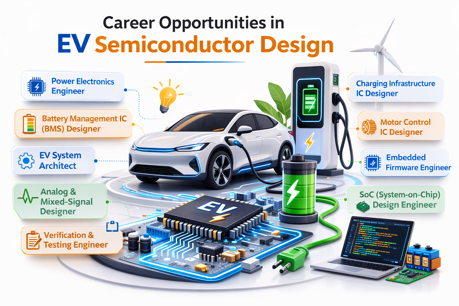
Career opportunities in EV semiconductor design are expanding rapidly as electric vehicle adoption accelerates worldwide. The growing complexity of automotive electronics—ranging from power management ICs and battery management systems (BMS) to ADAS processors and automotive networking chips—has created strong demand for skilled VLSI engineers, power electronics specialists, embedded system developers, and functional safety experts. Roles such as RTL Design Engineer, Physical Design Engineer, Verification Engineer, Analog/Mixed-Signal IC Designer, and Automotive SoC Architect are increasingly focused on EV-specific applications. Professionals with expertise in wide-bandgap semiconductors (SiC, GaN), high-voltage power device design, and ISO 26262 compliance are particularly valuable in 2026’s competitive semiconductor job market.
Beyond core chip design roles, EV semiconductor careers also extend into validation, reliability engineering, cybersecurity hardware design, and system-level integration. Engineers with knowledge of automotive communication protocols (CAN, Automotive Ethernet), battery modeling, thermal management, and AI accelerator design have strong growth prospects. As automotive OEMs collaborate more closely with semiconductor companies to develop custom chips for software-defined vehicles, interdisciplinary skills combining electronics, embedded software, and system architecture are becoming highly desirable. With increasing investments in EV manufacturing and semiconductor fabs globally, career pathways in EV semiconductor design offer long-term stability, competitive salaries, and opportunities to contribute to next-generation sustainable mobility technologies.
Conclusion
The rapid evolution of electric mobility has firmly established semiconductor design as the technological backbone of modern EVs. From power electronics and battery management systems to ADAS processors and high-speed automotive networking ICs, semiconductors directly influence vehicle efficiency, safety, performance, and connectivity. Innovations in wide-bandgap materials like SiC and GaN, centralized computing architectures, and AI-driven chip design methodologies are redefining how electric vehicles are engineered in 2026. As EV platforms shift toward higher voltage systems, ultra-fast charging, and software-defined architectures, advanced semiconductor solutions remain the key enabler of scalable, energy-efficient, and intelligent mobility.
Looking ahead, the synergy between automotive engineering and semiconductor innovation will continue to accelerate industry transformation. Strengthened supply chains, advanced packaging technologies, and AI-assisted VLSI workflows are reducing time-to-market while improving reliability and functional safety compliance. At the same time, expanding career opportunities in EV semiconductor design reflect the sector’s long-term growth potential. Ultimately, organizations and professionals that invest in next-generation automotive chip technologies will play a decisive role in shaping the future of sustainable transportation and intelligent electric vehicles.