
Top VLSI Backend Design Roles and Career Opportunities in 2026.
Navigate through this article using the table of contents below
Table of Contents
No headings found in this article.
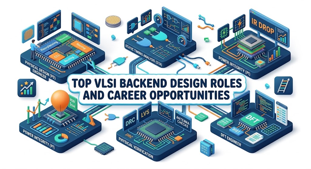
The semiconductor industry is evolving faster than ever, and VLSI backend design roles are becoming some of the most in-demand careers in the tech world. As chip complexity increases and advanced nodes like 5nm and 3nm become mainstream, companies are actively searching for skilled engineers who can handle physical design, timing closure, power optimization, and chip layout implementation. In 2026, the demand for VLSI backend design engineers is expected to grow significantly as industries such as AI, automotive electronics, IoT, and high-performance computing continue to rely on advanced semiconductor technologies.
From Physical Design Engineers and STA Engineers to DFT and Physical Verification specialists, VLSI backend design offers a wide range of high-paying and future-proof career opportunities. Professionals in these roles play a crucial part in transforming RTL designs into manufacturable silicon chips while ensuring performance, reliability, and efficiency. This blog explores the top VLSI backend design roles and career opportunities in 2026, highlighting the skills required, industry demand, and growth prospects for engineers aiming to build a successful career in the semiconductor industry.
What is VLSI Backend Design? Understanding the Physical Design Flow
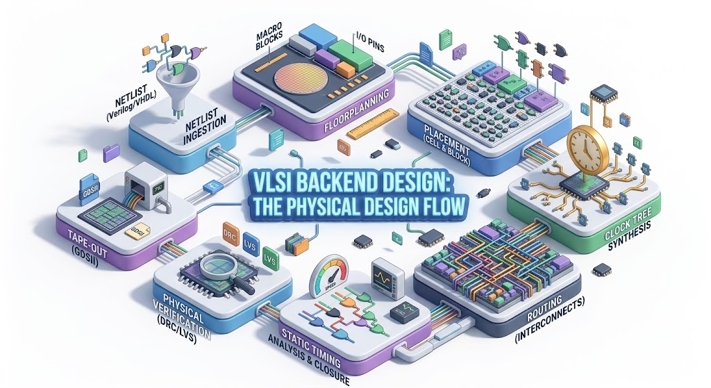
VLSI backend design is a critical stage in the semiconductor chip development process where the logical circuit design is transformed into a physical layout that can be manufactured on silicon. After the front-end design team completes the RTL design and functional verification, the backend design process begins with converting the synthesized netlist into an optimized chip layout. This stage focuses on implementing the design physically while ensuring timing, power, signal integrity, and area constraints are met. As modern chips become increasingly complex, VLSI backend design plays a vital role in ensuring that integrated circuits function efficiently and meet performance targets in real-world applications.
The physical design flow in VLSI backend design consists of several important stages, including floorplanning, placement, clock tree synthesis (CTS), routing, and physical verification. Floorplanning defines the chip’s structural layout and placement of major blocks, while placement arranges standard cells in optimal positions to minimize delays. Clock tree synthesis ensures proper distribution of the clock signal across the chip, and routing connects all the components using metal layers. Finally, physical verification steps such as Design Rule Check (DRC) and Layout vs. Schematic (LVS) ensure the layout meets manufacturing requirements. Understanding this physical design flow is essential for engineers who want to build a successful career in VLSI backend design and semiconductor engineering.
Why VLSI Backend Design Engineers Are in High Demand in 2026

The demand for VLSI backend design engineers is rapidly increasing in 2026 due to the growing complexity of semiconductor chips used in modern technologies. Industries such as artificial intelligence, high-performance computing, automotive electronics, 5G communication, and Internet of Things (IoT) devices require highly efficient and power-optimized integrated circuits. As chip designs move toward advanced process nodes like 5nm and 3nm, ensuring proper physical implementation, timing closure, and signal integrity becomes extremely challenging. This makes backend engineers essential because they convert logical designs into manufacturable silicon layouts while meeting strict performance, power, and area constraints.
Another major reason for the rising demand is the global expansion of the semiconductor ecosystem. Governments and technology companies are investing heavily in chip manufacturing and design to reduce supply chain dependencies and support emerging technologies. As a result, semiconductor companies are actively hiring physical design engineers, STA engineers, DFT specialists, and physical verification engineers to accelerate chip development cycles. Skilled backend engineers who can work with industry-standard tools and understand the full physical design flow are becoming highly valuable assets for semiconductor organizations.
Additionally, the shortage of experienced VLSI professionals has created significant career opportunities for engineers entering the field. Many semiconductor companies struggle to find engineers with strong expertise in timing analysis, floorplanning, routing optimization, and chip sign-off processes. This talent gap has led to competitive salaries, strong career growth, and global job opportunities in the semiconductor industry. For aspiring engineers, building expertise in VLSI backend design tools, scripting languages, and advanced physical design concepts can open the door to a stable and rewarding career in one of the fastest-growing technology sectors.
Physical Design Engineer: Roles, Responsibilities, and Skills Required
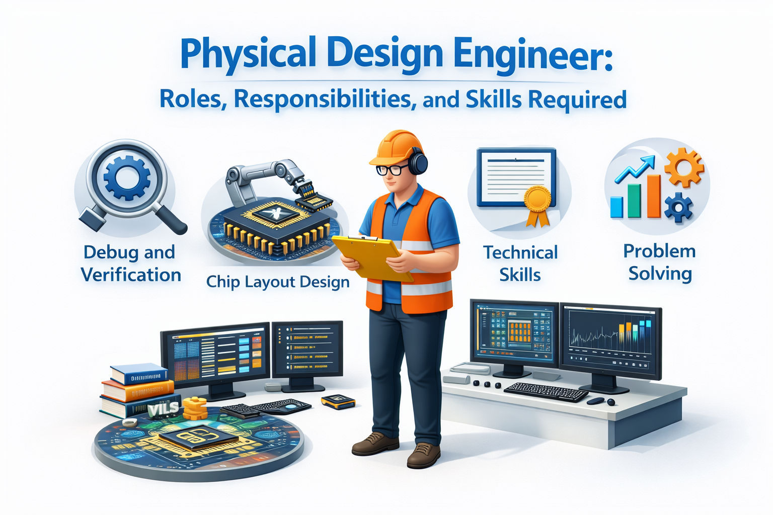
A Physical Design Engineer plays a crucial role in the VLSI backend design process by converting synthesized netlists into a complete physical layout that can be manufactured on silicon. Their primary responsibility is to implement the chip design while meeting strict constraints related to performance, power consumption, and chip area. The work typically involves several stages of the physical design flow, including floorplanning, placement, clock tree synthesis (CTS), routing, and timing optimization. Physical design engineers must also ensure that the design meets timing closure and signal integrity requirements while maintaining efficient power distribution and minimizing routing congestion across the chip.
To perform these tasks effectively, a physical design engineer must possess a combination of technical knowledge and practical tool expertise. Strong understanding of VLSI concepts such as timing analysis, clock distribution, parasitic effects, and power optimization is essential. Engineers also need hands-on experience with industry-standard EDA tools from major vendors such as Synopsys, Cadence Design Systems, and Siemens EDA (formerly Mentor Graphics). In addition, proficiency in scripting languages like Tcl, Python, or Perl is often required to automate design tasks and improve workflow efficiency. With the rapid advancement of semiconductor technologies, physical design engineers who develop strong problem-solving skills and stay updated with modern design methodologies can build a highly rewarding career in the semiconductor industry.
Essential Skills Required to Become a Successful VLSI Backend Engineer
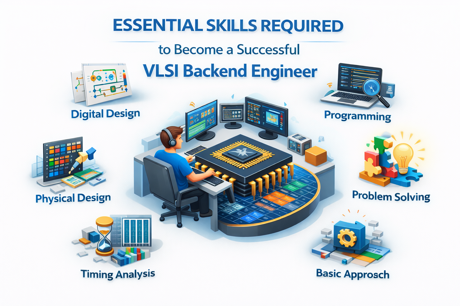
To become a successful VLSI backend engineer, a strong foundation in semiconductor fundamentals and digital design concepts is essential. Engineers must understand the complete physical design flow, including floorplanning, placement, clock tree synthesis (CTS), routing, and timing closure. Knowledge of important concepts such as setup and hold timing, signal integrity, power optimization, and parasitic effects is critical for ensuring that chip designs meet performance and reliability requirements. A deep understanding of CMOS technology, standard cell libraries, and advanced semiconductor nodes also helps engineers effectively implement complex integrated circuits in modern chip designs.
In addition to theoretical knowledge, backend engineers must develop strong expertise in industry-standard Electronic Design Automation (EDA) tools. Tools provided by companies like Synopsys, Cadence Design Systems, and Siemens EDA are widely used for physical design, timing analysis, and chip verification. Engineers should be comfortable working with tools for placement, routing, and static timing analysis, as well as performing physical verification checks such as Design Rule Check (DRC) and Layout vs. Schematic (LVS). Practical experience with these tools, often gained through academic projects, internships, or training programs, significantly increases employability in the semiconductor industry.
Another key requirement for VLSI backend engineers is strong programming and problem-solving ability. Scripting languages such as Tcl, Python, and Perl are commonly used to automate repetitive tasks, analyze design data, and improve workflow efficiency. Engineers also need analytical thinking skills to debug timing violations, optimize chip performance, and resolve design rule issues during the physical implementation process. Along with technical expertise, continuous learning and staying updated with evolving semiconductor technologies are important for long-term career growth in the highly competitive VLSI backend design field.
VLSI Backend Design Salary Trends in India and Globally (2026)

The salary trends for VLSI backend design engineers in 2026 remain highly competitive due to the growing demand for semiconductor professionals across the world. In India, entry-level backend engineers such as Physical Design, STA, or DFT engineers typically earn around ₹4 LPA to ₹6 LPA, while engineers with 2–5 years of experience can earn between ₹6 LPA and ₹15 LPA depending on their expertise and the company they work for. Senior engineers with more than five years of experience can command salaries ranging from ₹15 LPA to ₹35 LPA or more, especially in major semiconductor hubs like Bengaluru, Hyderabad, Pune, and Noida. Salaries also vary based on skills in timing closure, floorplanning, routing optimization, and proficiency with industry-standard EDA tools. (VLSI WEB)
At the entry level, fresh graduates entering the semiconductor industry in India are increasingly receiving competitive offers compared to many traditional engineering roles. Reports indicate that freshers working in semiconductor design roles can receive offers ranging from ₹6 LPA to ₹12 LPA, particularly from product-based semiconductor companies and global chip design firms. As engineers gain hands-on experience with backend design flows and tools, their earning potential increases significantly. The rapid expansion of India’s semiconductor ecosystem and government initiatives supporting chip manufacturing are also contributing to higher salaries and more job opportunities in this field. (The Times of India)
Globally, VLSI backend design engineers earn even higher salaries due to the strong demand for semiconductor expertise. In countries like the United States, experienced engineers working in physical design, STA, or ASIC implementation roles can earn between $100,000 and $170,000 per year, depending on experience and specialization. Engineers with advanced skills in advanced-node chip design, timing analysis, and physical verification often receive premium compensation packages that include bonuses and stock options. As technologies such as artificial intelligence, high-performance computing, and automotive electronics continue to grow, the global demand for skilled VLSI backend design professionals is expected to keep salaries rising in the coming years. (mosartlabs.com)
Career Path in VLSI Backend Design: Entry-Level to Senior Roles
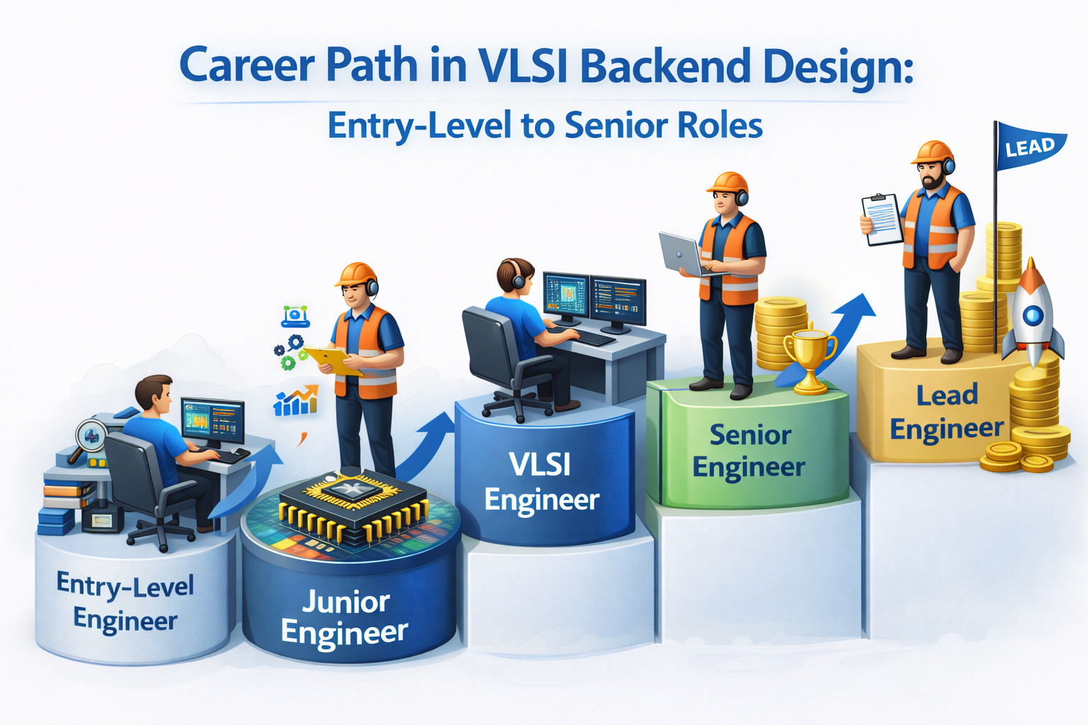
The career path in VLSI backend design typically begins with entry-level roles where engineers learn the fundamentals of the physical design flow and semiconductor implementation processes. Fresh graduates usually start as Junior Physical Design Engineers, Layout Engineers, or Physical Design Trainees, where they gain hands-on experience in tasks such as floorplanning, placement, routing, and basic timing analysis. At this stage, engineers work closely with senior team members while learning to use industry-standard EDA tools and understanding concepts like timing closure, signal integrity, and power optimization. Building strong technical skills and gaining practical project experience during this phase is essential for progressing in the semiconductor industry.
As engineers gain experience, they move into mid-level roles such as Physical Design Engineer, Static Timing Analysis (STA) Engineer, or DFT Engineer, where they handle more complex chip design tasks and contribute directly to chip implementation and optimization. With several years of experience, professionals can advance to senior positions like Senior Physical Design Engineer, Physical Design Lead, or ASIC Implementation Engineer, where they manage critical design blocks and mentor junior engineers. Eventually, experienced professionals may progress to leadership roles such as Physical Design Manager, VLSI Architect, or Technical Director, overseeing entire chip development projects and guiding the backend design strategy for advanced semiconductor products.
Best Projects to Build a Strong VLSI Backend Design Resume
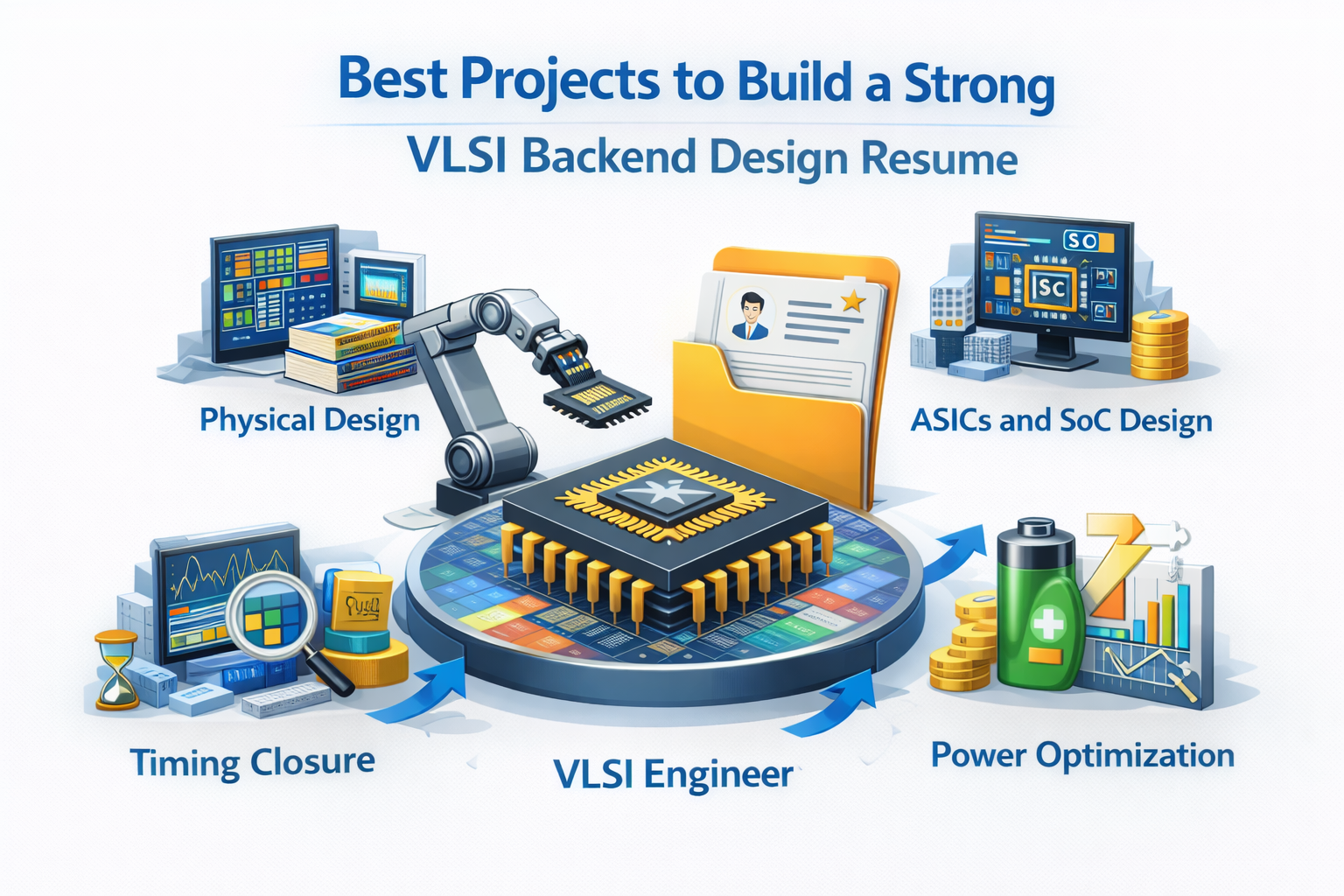
Building a strong VLSI backend design resume requires practical project experience that demonstrates your understanding of the physical design flow and semiconductor implementation concepts. One of the most valuable projects is implementing a complete ASIC physical design flow for a simple digital block, such as an ALU, multiplier, or RISC-based processor module. In this type of project, engineers perform key stages including floorplanning, placement, clock tree synthesis (CTS), routing, and timing analysis. Completing a full physical design project shows recruiters that you understand how to convert a synthesized netlist into a manufacturable chip layout while meeting performance, power, and area constraints.
Another highly recommended project involves Static Timing Analysis (STA) and timing closure optimization. In this project, engineers analyze timing reports, identify setup and hold violations, and apply optimization techniques to meet timing requirements. This helps demonstrate expertise in critical backend concepts such as clock skew, propagation delay, and timing constraints. Learning to use professional Electronic Design Automation (EDA) tools from companies like Synopsys and Cadence Design Systems during these projects adds significant value to a resume because these tools are widely used across the semiconductor industry.
Additionally, projects focused on physical verification and design rule checking can greatly strengthen a VLSI backend portfolio. For example, performing Design Rule Check (DRC), Layout vs. Schematic (LVS), and parasitic extraction on a chip layout helps engineers understand the manufacturing constraints involved in semiconductor fabrication. Such projects highlight a candidate’s ability to ensure layout accuracy and reliability before tape-out. By including multiple hands-on projects that cover different stages of the backend design flow, aspiring engineers can create a compelling resume that demonstrates both technical knowledge and practical experience in the VLSI backend design domain.
Future Scope of VLSI Backend Design in the Semiconductor Industry

The future scope of VLSI backend design in the semiconductor industry looks extremely promising as the demand for advanced chips continues to grow across multiple technology sectors. Industries such as artificial intelligence, autonomous vehicles, high-performance computing, 5G communication, and Internet of Things (IoT) devices rely heavily on highly optimized semiconductor chips. As chip designs move toward advanced technology nodes and become more complex, the role of backend engineers becomes increasingly critical. They are responsible for ensuring that chip layouts meet strict performance, power, and manufacturing requirements, making VLSI backend design an essential and future-proof career path in the semiconductor ecosystem.
In addition, global investments in semiconductor manufacturing and chip design are creating new opportunities for skilled backend professionals. Many technology companies and semiconductor firms are expanding their research and development centers to accelerate chip innovation and reduce supply chain dependencies. As a result, engineers with expertise in physical design, timing analysis, and physical verification will continue to be in high demand worldwide. With continuous advancements in chip architecture and semiconductor technologies, professionals who develop strong backend design skills and stay updated with modern design tools can expect long-term career growth and exciting opportunities in the evolving VLSI and semiconductor industry.
Tips to Start a Career in VLSI Backend Design for Beginners
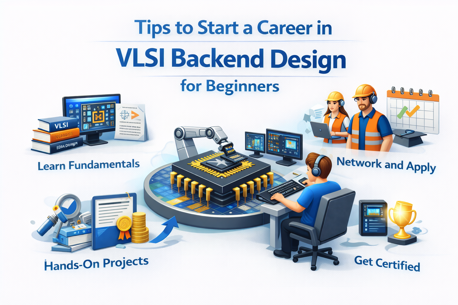
Starting a career in VLSI backend design requires a strong understanding of digital electronics, semiconductor fundamentals, and the physical design flow. Beginners should first focus on learning core concepts such as CMOS technology, standard cell libraries, timing analysis, and chip layout fundamentals. Understanding the stages of the backend flow—floorplanning, placement, clock tree synthesis (CTS), routing, and physical verification—is essential for building a solid foundation. Students and aspiring engineers can strengthen their knowledge through online courses, university labs, and technical resources that cover modern VLSI design methodologies used in the semiconductor industry.
In addition to theoretical learning, gaining hands-on experience with industry-standard Electronic Design Automation (EDA) tools is crucial for entering this field. Tools from companies like Synopsys, Cadence Design Systems, and Siemens EDA are widely used for physical design and chip verification. Beginners should also work on practical projects, learn scripting languages such as Tcl or Python, and practice analyzing timing and layout reports. Building a strong portfolio of VLSI projects and staying updated with the latest semiconductor technologies can significantly improve job prospects and help beginners successfully start a career in VLSI backend design.
Conclusion
A career as a VLSI Verification Engineer plays a crucial role in the semiconductor industry, ensuring that complex chip designs function correctly before they are manufactured. As modern electronic devices become more advanced, the demand for skilled verification engineers continues to grow across global semiconductor companies. By understanding the VLSI design flow, mastering verification methodologies, and developing strong debugging and analytical skills, aspiring engineers can build a solid foundation in this highly specialized field. With the right educational background and hands-on project experience, entering the VLSI verification domain can open doors to exciting opportunities in cutting-edge technology development.
In addition to strong technical knowledge, continuous learning and practical exposure are essential for long-term success in this career path. Engineers who stay updated with emerging verification tools, methodologies like SystemVerilog and UVM, and evolving semiconductor technologies can significantly enhance their professional growth. With competitive salaries, clear career progression, and increasing demand in areas such as AI hardware, automotive electronics, and advanced SoC design, VLSI verification offers a promising and rewarding career for electronics and semiconductor engineers worldwide.