

Ultimate Guide to RTL Design Engineer Training: Skills, Syllabus & Job Scope
Navigate through this article using the table of contents below
Table of Contents
No headings found in this article.
The semiconductor industry is evolving at an unprecedented pace—and at the heart of every high-performance chip lies a skilled RTL Design Engineer. If you’re aiming to build a career in VLSI or digital IC design, mastering Register Transfer Level (RTL) design is the critical first step. This Ultimate Guide to RTL Design Engineer Training: Skills, Syllabus & Job Scope will walk you through everything you need to know, from core technical competencies to structured learning paths and real-world career opportunities in the semiconductor domain. To build a strong foundation in modern chip design, you can start with an industry-focused RTL Design Engineer Training program.
RTL Design Engineer training focuses on building strong fundamentals in digital electronics, Verilog/SystemVerilog coding, simulation, synthesis, timing analysis, and FPGA/ASIC design flow. A well-structured syllabus not only covers HDL programming and RTL coding guidelines but also emphasizes industry tools, debugging methodologies, and project-based learning aligned with current semiconductor standards. In this guide, you will explore essential RTL design skills, detailed course modules, job roles, salary scope, and future growth opportunities—helping you make informed decisions and strategically plan your career in VLSI and chip design.
What is RTL Design? Understanding Register Transfer Level in VLSI
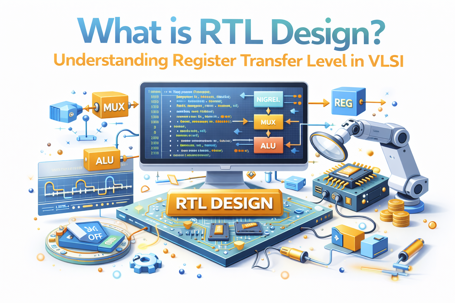
RTL (Register Transfer Level) Design is a hardware abstraction methodology used in VLSI (Very Large Scale Integration) to model digital circuits in terms of data flow between registers and the logical operations performed on that data. At the RTL level, designers describe how data moves between registers on clock edges and how combinational logic transforms that data. This abstraction sits between high-level behavioral design and gate-level implementation, making it a critical stage in the digital IC design flow. RTL design is typically written using Hardware Description Languages (HDLs) such as Verilog or SystemVerilog, allowing engineers to simulate, verify, and synthesize digital systems before physical implementation.
In the VLSI design flow, RTL serves as the foundation for ASIC and FPGA development. Once the design specification is defined, engineers create RTL code that represents the intended functionality of the chip. This code is then verified through simulation, synthesized into gate-level netlists, and later passed to physical design stages. A well-written RTL design ensures optimal timing, area efficiency, and power consumption, directly impacting chip performance and manufacturability. Understanding RTL design is essential for anyone pursuing a career as an RTL Design Engineer, as it bridges theoretical digital electronics concepts with real-world semiconductor product development.
Who is an RTL Design Engineer? Roles and Responsibilities

An RTL Design Engineer is a semiconductor professional responsible for designing and implementing digital hardware systems at the Register Transfer Level (RTL) using Hardware Description Languages such as Verilog or SystemVerilog. Working within the VLSI design domain, RTL engineers translate architectural specifications into synthesizable RTL code that defines how data flows between registers and how logical operations are executed on clock cycles. Their work forms the functional backbone of ASIC and FPGA designs, making them a core part of any chip development team.
The primary roles and responsibilities of an RTL Design Engineer include writing clean, efficient, and synthesizable RTL code, designing modules such as controllers, datapaths, finite state machines (FSMs), and memory interfaces, and ensuring compliance with timing, power, and area constraints. They perform functional simulation, debug design issues, analyze waveforms, and collaborate closely with verification engineers to validate functionality. RTL engineers also work with synthesis and static timing analysis (STA) tools to ensure that the design meets performance targets and integrates correctly within the larger SoC architecture.
Beyond coding, RTL Design Engineers participate in design reviews, micro-architecture discussions, and cross-functional coordination with physical design, DFT, and verification teams. They are responsible for maintaining coding standards, resolving clock domain crossing (CDC) issues, optimizing resource utilization, and ensuring that the design is scalable and reusable. Strong analytical skills, deep knowledge of digital electronics, and proficiency in EDA tools are essential for excelling in this role and building a successful career in VLSI and semiconductor design.
Why Choose a Career as an RTL Design Engineer in 2026?

Choosing a career as an RTL Design Engineer in 2026 offers strong long-term growth due to the rapid expansion of the global semiconductor industry. With increasing demand for AI accelerators, automotive electronics, 5G infrastructure, IoT devices, and high-performance computing systems, companies are investing heavily in custom chip development. RTL design sits at the core of digital IC development, making skilled RTL engineers essential for translating system architecture into silicon-ready implementations. As nations prioritize semiconductor self-reliance and chip innovation, career stability and global opportunities in VLSI design continue to expand. Training institutes like JastTech are also helping aspiring engineers build industry-ready RTL design skills aligned with current market demands.
From a technical perspective, RTL Design Engineering provides deep exposure to digital system architecture, micro-architecture development, and ASIC/FPGA design flows. Engineers gain expertise in Verilog/SystemVerilog coding, simulation, synthesis, timing analysis, and design optimization—skills that are highly valued across product-based semiconductor companies. Unlike some software roles that evolve rapidly with frameworks and platforms, RTL design is grounded in strong digital fundamentals, making it a technically resilient and future-proof career path. The role also offers opportunities to transition into advanced domains such as SoC architecture, low-power design, or design leadership.
Financially and professionally, RTL Design Engineers benefit from competitive salary packages, especially in semiconductor hubs such as India, the United States, and Europe. With experience, professionals can move into senior design roles, chip architects, or technical leads within leading fabless and product companies. As semiconductor complexity increases with advanced nodes and heterogeneous integration, the demand for high-quality RTL talent is expected to remain strong beyond 2026. For individuals passionate about hardware, digital logic, and chip design, RTL engineering represents a high-impact and future-oriented career choice.
Core Skills Required for RTL Design Engineers
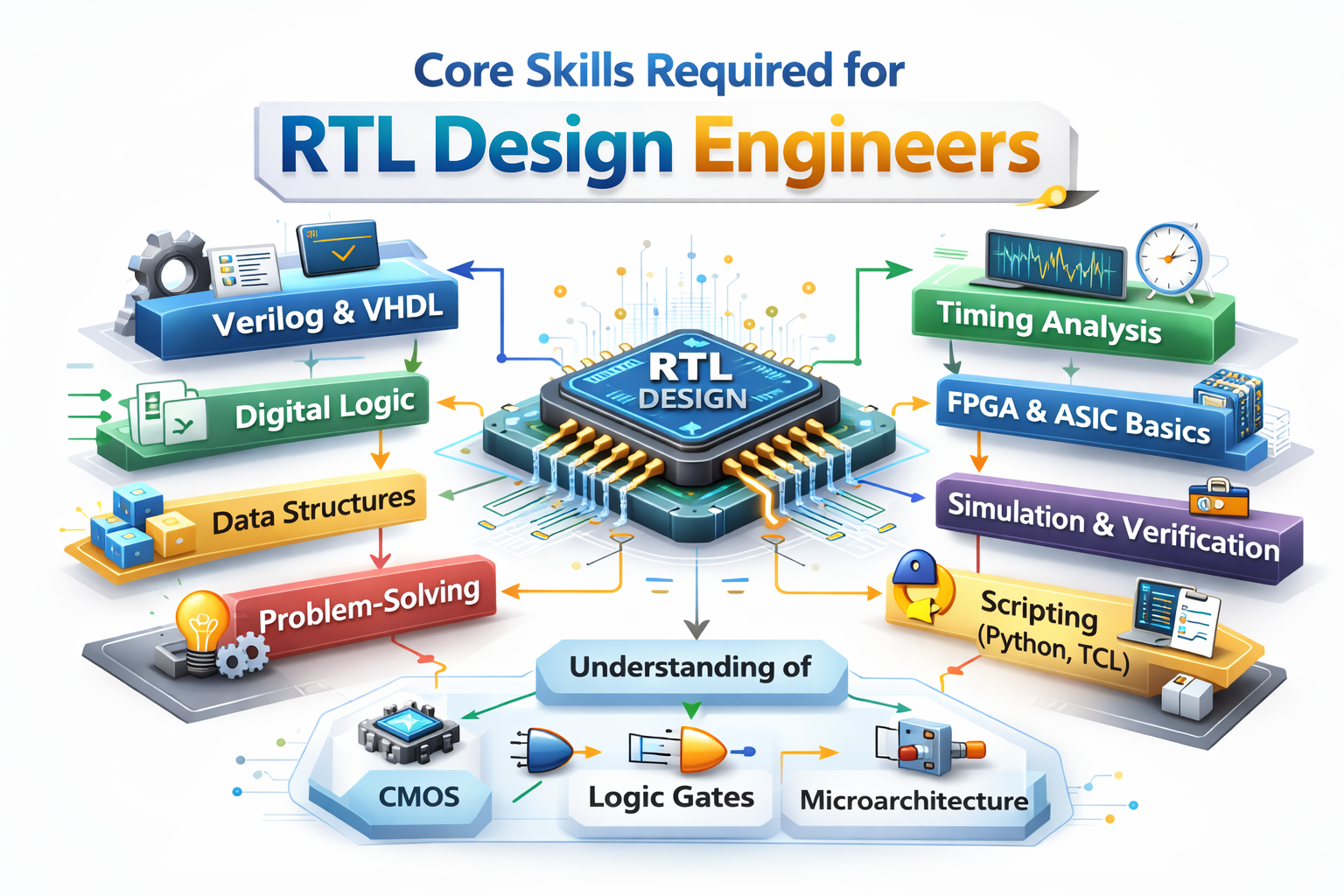
To succeed as an RTL Design Engineer, a strong foundation in digital electronics is essential. Engineers must thoroughly understand combinational and sequential logic, flip-flops, multiplexers, encoders, decoders, counters, and finite state machines (FSMs). Concepts such as setup and hold time, clocking mechanisms, metastability, and timing diagrams are critical for writing reliable and synthesizable RTL code. A deep grasp of Boolean algebra, number systems, and micro-architecture principles enables engineers to translate functional specifications into efficient hardware implementations aligned with ASIC and FPGA design methodologies.
Proficiency in Hardware Description Languages (HDLs) such as Verilog and SystemVerilog is a core technical requirement. RTL Design Engineers must be skilled in writing synthesizable RTL, developing parameterized modules, handling clock domain crossing (CDC) scenarios, and following industry-standard coding guidelines. Expertise in simulation, waveform debugging, and testbench basics is equally important to validate functionality before synthesis. Additionally, familiarity with EDA tools for simulation, synthesis, and static timing analysis (STA) allows engineers to optimize designs for performance, power, and area constraints.
Beyond technical knowledge, strong analytical thinking and problem-solving skills are vital in RTL design. Engineers must interpret design specifications accurately, identify corner-case scenarios, debug functional mismatches, and collaborate effectively with verification, physical design, and DFT teams. Understanding design for scalability, low-power techniques, and reusable IP development further enhances career prospects. Combining solid digital fundamentals with practical tool experience and structured debugging skills ensures long-term success in the competitive VLSI and semiconductor industry.
RTL Design Flow: From Specification to Silicon
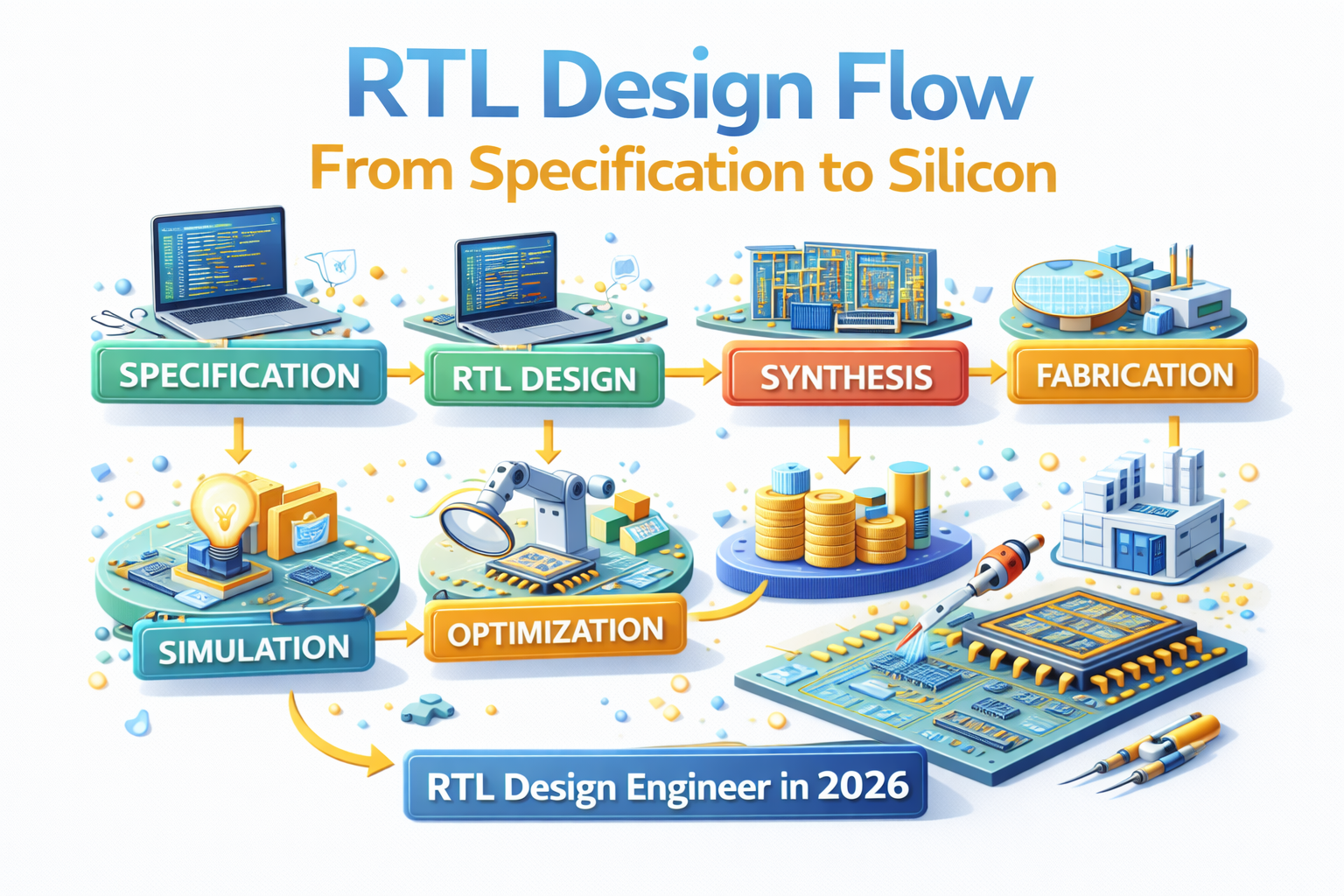
The RTL design flow begins with a detailed functional specification that defines the architecture, performance targets, power constraints, and interface requirements of the digital system. Based on this specification, RTL Design Engineers develop the micro-architecture and write synthesizable RTL code using Verilog or SystemVerilog. The design is then validated through functional simulation, where testbenches are used to verify correctness and identify corner-case bugs. Once the RTL passes verification, it is synthesized into a gate-level netlist using synthesis tools, ensuring that timing, area, and power constraints are met. Static Timing Analysis (STA) is performed to validate timing closure before moving to the physical implementation stage.
After synthesis, the design proceeds to physical design, which includes floorplanning, placement, clock tree synthesis (CTS), routing, and physical verification checks such as DRC and LVS. Post-layout simulations and timing analysis ensure that the design maintains functional integrity under real silicon conditions. Once all sign-off criteria are satisfied, the design moves to tape-out, where the final GDSII file is sent for fabrication. This complete journey—from specification to silicon—requires close collaboration between RTL, verification, physical design, and DFT teams, making the RTL stage a foundational pillar in successful ASIC and FPGA development.
Difference Between RTL Design and Verification
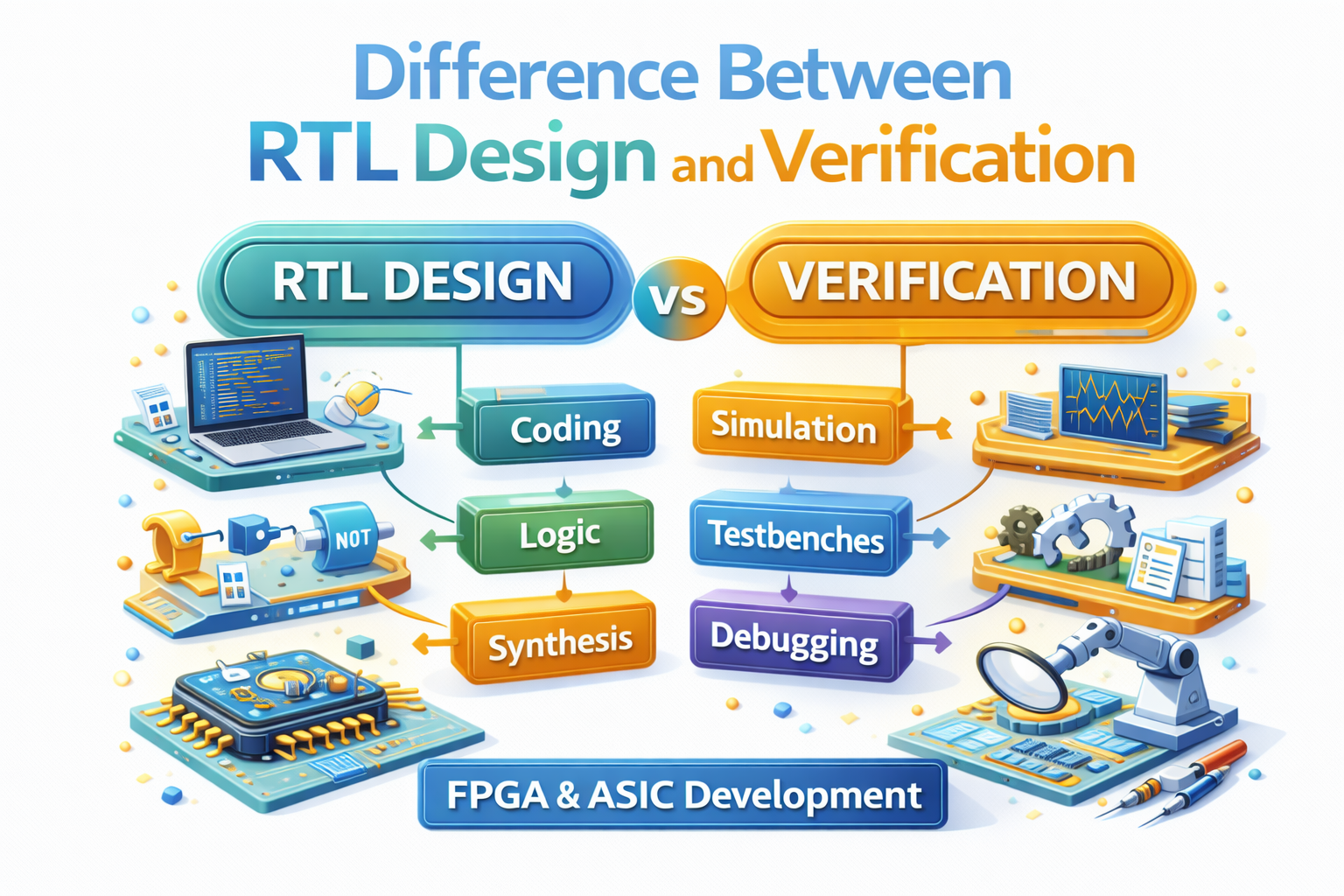
The primary difference between RTL Design and Verification lies in their core objectives within the VLSI design flow. RTL Design focuses on creating the hardware functionality by writing synthesizable code in Verilog or SystemVerilog that defines how data moves between registers and how logic operates on clock cycles. In contrast, Verification ensures that the RTL implementation behaves exactly as intended according to the design specification. While RTL engineers build the digital architecture, verification engineers validate its correctness, reliability, and compliance before the design moves to synthesis and physical implementation.
From a skill-set perspective, RTL Design Engineers require strong knowledge of digital electronics, micro-architecture development, timing analysis, and synthesis concepts. Their work emphasizes writing optimized, clean, and hardware-efficient RTL code that meets power, performance, and area (PPA) constraints. Verification Engineers, on the other hand, specialize in advanced simulation methodologies, testbench development, SystemVerilog assertions, coverage analysis, and often use frameworks such as UVM (Universal Verification Methodology). Their goal is to detect design bugs, validate corner cases, and ensure functional completeness before silicon fabrication.
Career growth and work dynamics also differ between the two roles. RTL Design is closely tied to architecture decisions and hardware implementation, making it ideal for individuals passionate about digital circuit creation and chip design. Verification typically involves extensive debugging, stimulus generation, and coverage-driven validation, offering broader exposure to system-level behavior and advanced verification methodologies. Both roles are critical in semiconductor development, and the choice between RTL Design and Verification depends on whether one prefers building digital hardware logic or rigorously testing and validating complex designs.
RTL Design Engineer Salary in India and Globally
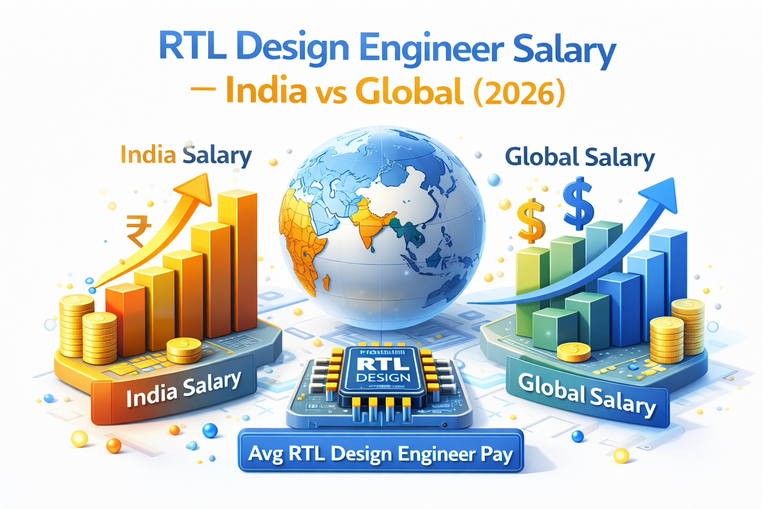
RTL Design Engineer salaries in India reflect the strong demand for skilled semiconductor professionals in major tech hubs such as Bangalore, Hyderabad, Pune, and Noida. Entry-level RTL engineers with 0–2 years of experience typically earn competitive packages compared to other engineering disciplines, with salaries increasing significantly as they gain proficiency in HDL coding, synthesis, and timing analysis. Mid-level engineers with 3–6 years of experience often move into senior design roles or technical leads, commanding higher compensation due to their practical expertise in ASIC/FPGA flows and EDA tools. In India, additional benefits such as performance bonuses, stock options (in product companies), and relocation support further enhance total remuneration for experienced RTL design talent.
Globally, RTL Design Engineers are among the better-paid professionals in the semiconductor sector, especially in regions with a deep presence of chip design and fabless companies such as the United States, Germany, Taiwan, South Korea, and Japan. In North America and Europe, senior RTL engineers and architects working on advanced nodes (5 nm, 3 nm) or specialized domains like high-speed IO, low-power design, or AI accelerators often receive premium compensation packages, including base salary, bonuses, and equity. Global mobility, expertise in industry tools (e.g., Synopsys, Cadence), and experience with complex SoC designs contribute to higher earning potential. Overall, mastering RTL design skills can open doors to lucrative career opportunities both within India and internationally as semiconductor demand continues its long-term upward trajectory.
How to Become an RTL Design Engineer: Step-by-Step Roadmap
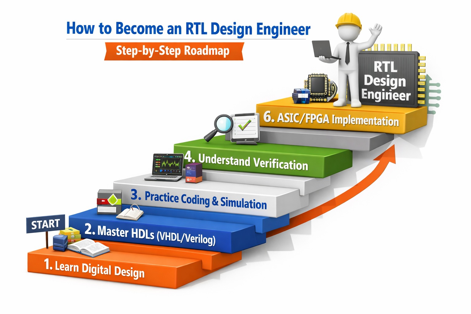
Becoming an RTL Design Engineer requires a structured learning approach starting with strong fundamentals in digital electronics and computer architecture. The first step is mastering core concepts such as combinational and sequential circuits, flip-flops, finite state machines (FSMs), number systems, and timing analysis. A solid understanding of microprocessors, memory architecture, and digital system design builds the conceptual base needed for RTL development. Students pursuing Electronics, ECE, or related engineering degrees should focus on subjects aligned with VLSI and semiconductor design while strengthening problem-solving and analytical skills.
The second step is gaining hands-on expertise in Hardware Description Languages (HDLs) such as Verilog and SystemVerilog. Learn how to write synthesizable RTL code, design modular architectures, and follow industry-standard coding guidelines. Practical exposure to simulation tools, waveform debugging, and synthesis flows is critical. Work on projects like UART, FIFO, SPI controller, or simple RISC processor design to build a strong portfolio. Understanding the RTL design flow—from specification to simulation, synthesis, and static timing analysis (STA)—is essential for real-world readiness in ASIC or FPGA development environments.
The final step involves industry preparation and career positioning. Gain internship experience in semiconductor or VLSI companies to understand collaborative workflows between RTL, verification, and physical design teams. Prepare for technical interviews by revising digital concepts, HDL coding patterns, and debugging scenarios. Stay updated with semiconductor trends such as low-power design, clock domain crossing (CDC), and SoC integration. With consistent practice, project experience, and tool proficiency, aspiring engineers can successfully transition into entry-level RTL Design Engineer roles and build a long-term career in the semiconductor industry.
Best Projects for RTL Design Engineer Resume
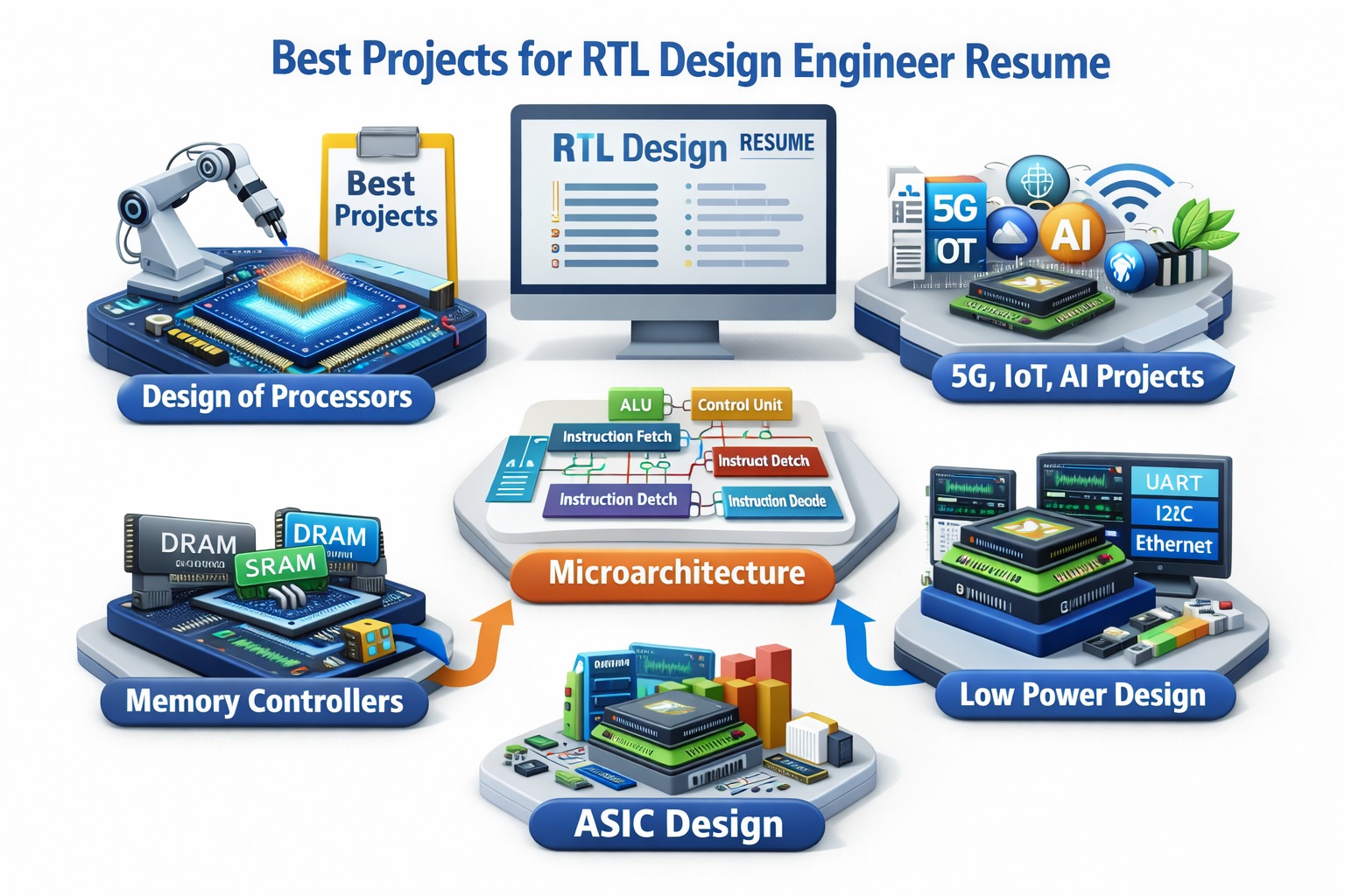
Including strong, implementation-focused projects on an RTL Design Engineer resume significantly increases your credibility in the VLSI job market. Ideal projects should demonstrate your ability to write synthesizable Verilog/SystemVerilog code, design modular architectures, and validate functionality through simulation. High-impact RTL projects include UART design, SPI/I2C controller implementation, FIFO memory design with proper clock domain handling, ALU design, and finite state machine (FSM)-based controllers. These projects showcase your understanding of sequential logic, data path design, and timing concepts—core competencies required in ASIC and FPGA development roles.
For advanced differentiation, consider implementing a simple RISC processor, pipelined CPU architecture, or cache controller with basic memory interfacing. Projects that include synthesis reports, timing analysis, and FPGA prototyping demonstrate practical exposure to the complete RTL design flow. Clearly mention design specifications, challenges faced (such as setup/hold violations or CDC issues), and how you optimized for performance, power, or area. Recruiters in semiconductor companies value candidates who can move beyond theoretical knowledge and prove hands-on RTL coding, debugging, and hardware validation experience through well-documented, industry-relevant projects.
Future Scope of RTL Design Engineering in the Semiconductor Industry
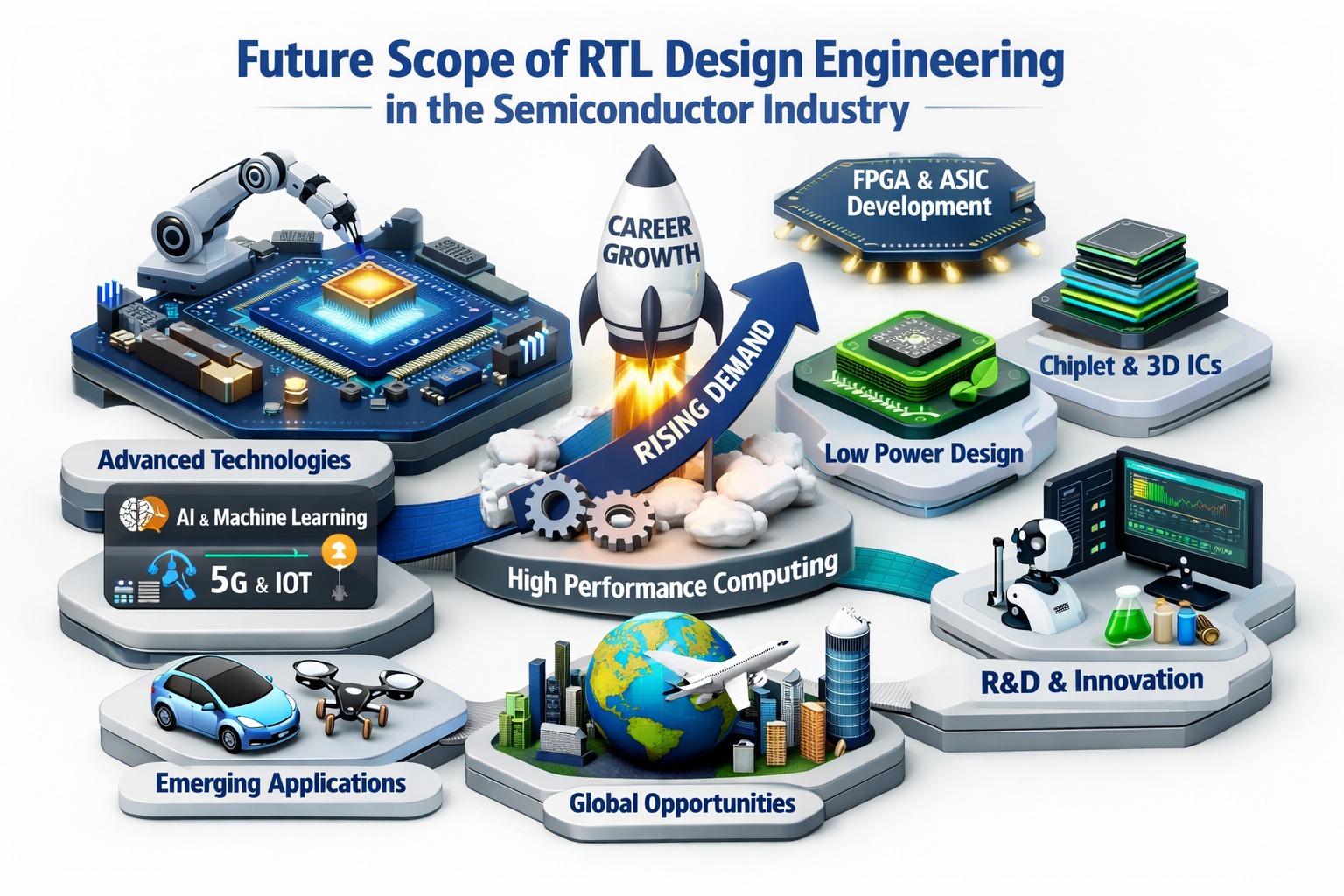
The future scope of RTL Design Engineering in the semiconductor industry remains highly promising as global demand for advanced chips continues to accelerate. Emerging technologies such as artificial intelligence accelerators, autonomous vehicles, 5G/6G communication systems, IoT devices, and high-performance computing platforms rely heavily on complex digital architectures implemented at the RTL level. As chip designs grow more sophisticated with heterogeneous integration and advanced process nodes, the need for skilled RTL engineers who can develop optimized, power-efficient, and high-performance digital logic is steadily increasing across global semiconductor hubs.
Technological advancements are further expanding the role of RTL engineers beyond traditional ASIC development. Modern System-on-Chip (SoC) designs integrate CPUs, GPUs, AI engines, memory subsystems, and high-speed interfaces, all of which require precise RTL implementation and integration. Low-power design techniques, clock domain crossing management, design for testability (DFT), and performance-driven micro-architecture optimization are becoming critical competencies. Engineers who continuously upgrade their skills in SystemVerilog, synthesis methodologies, and advanced design flows will remain highly competitive in the evolving semiconductor ecosystem.
From a career growth perspective, RTL Design Engineering offers long-term stability and upward mobility. Professionals can transition into senior design roles, SoC architecture, technical leadership, or specialized domains such as high-speed interface design and AI hardware acceleration. As countries invest heavily in domestic semiconductor manufacturing and chip innovation, opportunities in both India and international markets are expected to expand. With the semiconductor industry projected to grow significantly over the next decade, RTL design expertise will continue to be a cornerstone skill driving next-generation silicon development.
Conclusion
RTL Design Engineering stands at the core of modern semiconductor innovation, forming the critical bridge between digital architecture and physical silicon implementation. From understanding RTL fundamentals and mastering Verilog/SystemVerilog to learning synthesis, timing analysis, and real-world design flow, the journey to becoming a successful RTL Design Engineer requires structured training and consistent hands-on practice. As discussed throughout this guide, building strong digital fundamentals, developing practical project experience, and understanding industry tools are essential steps toward establishing a rewarding career in VLSI and chip design.
With the semiconductor industry expanding rapidly across AI, automotive electronics, 5G, IoT, and high-performance computing, the demand for skilled RTL professionals continues to rise globally. Competitive salaries, long-term career stability, and opportunities to work on cutting-edge silicon technologies make RTL Design Engineering a highly promising career path. By following a clear roadmap, continuously upgrading technical skills, and staying aligned with industry trends, aspiring engineers can position themselves strongly for success in the evolving world of semiconductor design.