

VLSI CAD Engineer Career Guide: Tools, Skills, and Industry Scope
Navigate through this article using the table of contents below
Table of Contents
No headings found in this article.
The semiconductor industry is evolving rapidly, and behind every successful chip design lies a powerful set of tools and experts who manage them. VLSI CAD engineers play a crucial role in enabling efficient chip development by building, maintaining, and optimizing Electronic Design Automation (EDA) tools used throughout the VLSI design flow. From RTL development and synthesis to physical design and verification, CAD engineers ensure that design teams can work faster, automate complex processes, and achieve high-quality silicon. As semiconductor companies continue to push toward smaller technology nodes and more complex chip architectures, the demand for skilled VLSI CAD engineers is growing rapidly across the global semiconductor ecosystem.
In this VLSI CAD Engineer Career Guide, we explore the essential tools, technical skills, and industry opportunities that define this specialized role in the semiconductor industry. CAD engineers act as the bridge between design engineers and EDA tools, helping optimize workflows, develop automation scripts, and improve productivity across large chip design projects. Understanding the responsibilities, required programming knowledge, and commonly used tools such as Synopsys, Cadence, and Mentor Graphics can help aspiring engineers build a strong career path in this field. This guide will help you understand the scope, career growth, and future opportunities for VLSI CAD engineers in the rapidly expanding semiconductor industry.
What is a VLSI CAD Engineer? Understanding the Role in Chip Design

A VLSI CAD (Computer-Aided Design) Engineer is a specialized professional in the semiconductor industry who develops, maintains, and optimizes the software tools and automation flows used in chip design. In modern VLSI design, engineers rely heavily on Electronic Design Automation (EDA) tools to handle complex processes such as RTL design, synthesis, verification, timing analysis, and physical layout. A VLSI CAD engineer ensures that these tools work efficiently across the design flow, helping design teams improve productivity, reduce errors, and accelerate chip development cycles. By creating automated scripts, integrating new EDA tools, and optimizing design workflows, CAD engineers play a crucial role in enabling large-scale semiconductor projects.
In the chip design process, VLSI CAD engineers act as the bridge between hardware design engineers and EDA software tools. They support multiple teams—including RTL designers, verification engineers, and physical design engineers—by developing automated flows, debugging tool-related issues, and ensuring smooth tool integration across complex design environments. Their work often involves programming and scripting using languages such as Python, TCL, Perl, and Shell to automate repetitive tasks and improve design efficiency. As semiconductor designs become more complex with advanced technology nodes and large system-on-chip (SoC) architectures, the role of VLSI CAD engineers has become increasingly important in ensuring reliable, scalable, and high-performance chip development.
Importance of CAD Engineering in the VLSI Design Flow
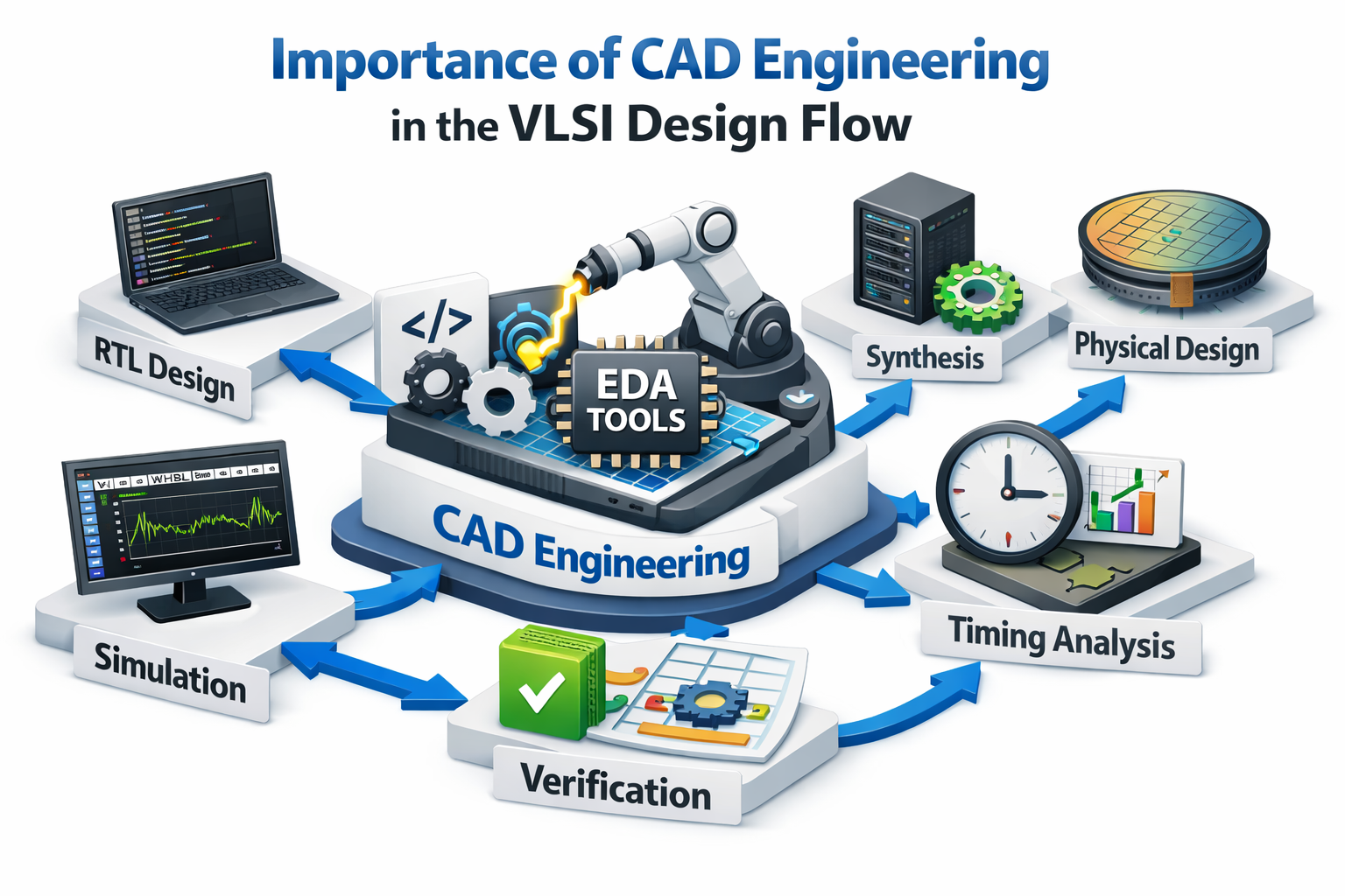
CAD engineering plays a critical role in the VLSI design flow, enabling semiconductor companies to design complex integrated circuits efficiently and accurately. Modern chip development involves multiple stages such as RTL design, simulation, synthesis, timing analysis, physical design, and verification. Each of these stages depends heavily on Electronic Design Automation (EDA) tools to manage billions of transistors and highly complex architectures. VLSI CAD engineers ensure that these tools are properly configured, integrated, and optimized so that design teams can execute their workflows smoothly without delays or technical bottlenecks.
One of the most important contributions of CAD engineering is automation of design flows. VLSI design projects involve repetitive and computationally intensive tasks that must be executed with precision. CAD engineers create automated scripts and workflows using languages such as Python, TCL, and Shell scripting to streamline these processes. Automation not only reduces manual effort but also improves consistency, reduces human errors, and accelerates the chip development cycle. This efficiency is crucial for semiconductor companies that must meet tight deadlines while maintaining high design quality.
Additionally, CAD engineering ensures scalability and tool optimization in large semiconductor projects. As chips move to advanced technology nodes like 5nm, 3nm, and beyond, the complexity of design and verification increases significantly. CAD engineers work to optimize tool performance, manage large datasets, and integrate multiple EDA tools across the design environment. Their expertise helps design teams handle large-scale System-on-Chip (SoC) designs more effectively, making CAD engineering an essential component of the modern semiconductor design ecosystem.
Essential Programming Skills Required for VLSI CAD Engineers
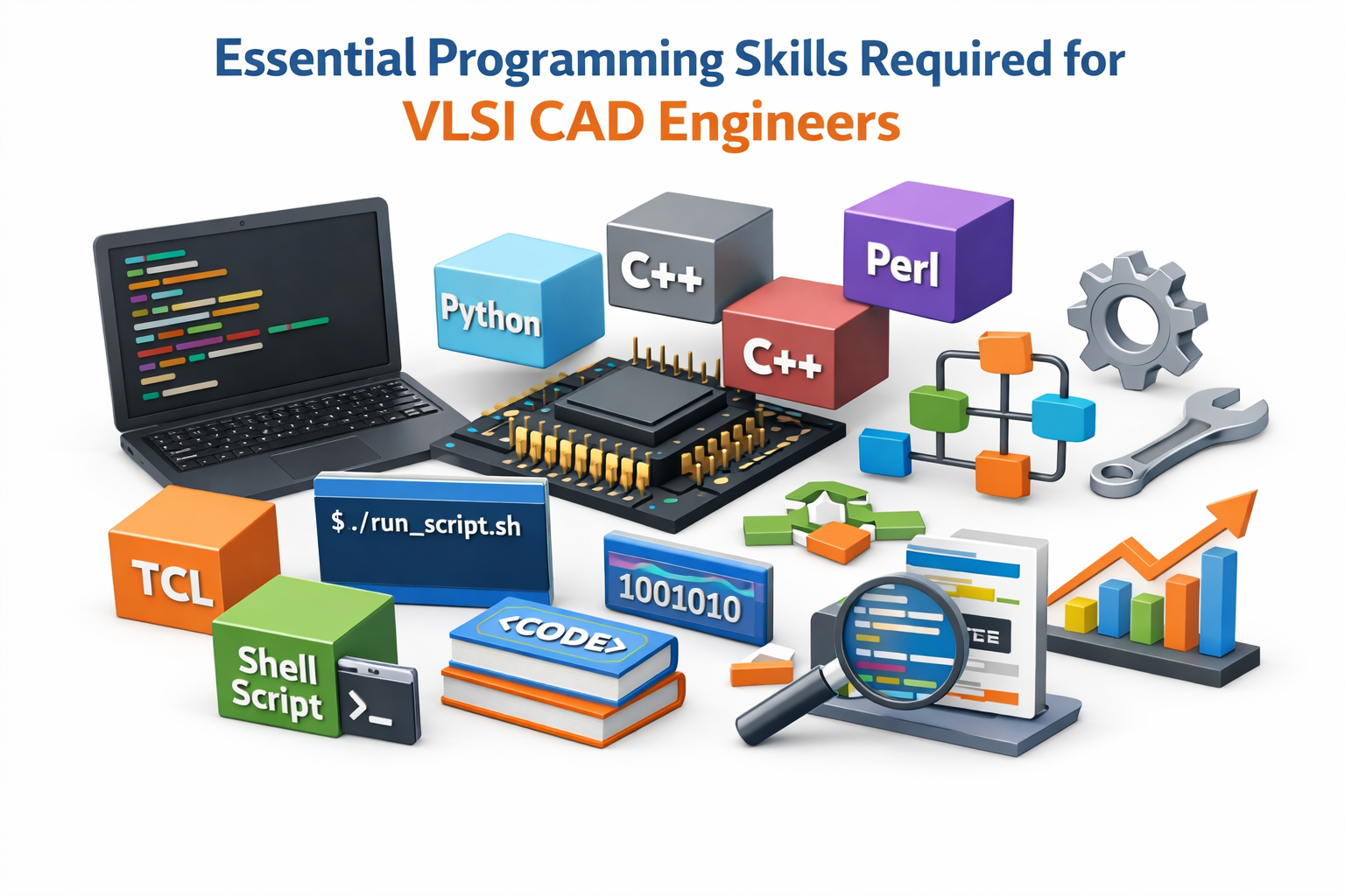
Programming skills are fundamental for VLSI CAD engineers because their primary responsibility is to automate, customize, and optimize Electronic Design Automation (EDA) tools used in semiconductor design. One of the most important scripting languages in the VLSI industry is TCL (Tool Command Language), which is widely used to control and automate EDA tools from companies like Cadence, Synopsys, and Siemens EDA. CAD engineers use TCL scripts to automate design flows, manage tool configurations, and execute repetitive tasks across large chip design projects. Additionally, Shell scripting is commonly used in Linux-based design environments to manage workflows, run batch processes, and integrate different stages of the VLSI design flow.
Beyond scripting, high-level programming languages such as Python, Perl, and C/C++ are also essential for VLSI CAD engineers. Python is increasingly popular for developing automation frameworks, data analysis scripts, and workflow management systems within semiconductor design teams. Perl has traditionally been used for text processing and automation in many existing EDA flows, while C/C++ is often required for developing performance-critical tools or extending EDA functionalities. Strong programming knowledge enables CAD engineers to build efficient automation systems, troubleshoot tool-related issues, and improve overall productivity in complex chip design environments.
Popular EDA Tools Used by VLSI CAD Engineers
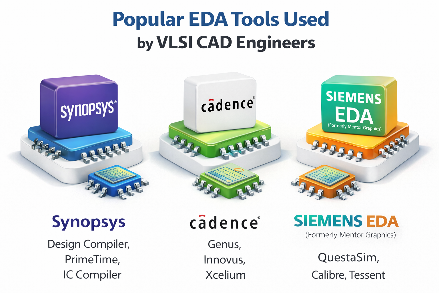
Electronic Design Automation (EDA) tools are essential for designing, verifying, and optimizing modern integrated circuits, and VLSI CAD engineers play a key role in managing these tools within the semiconductor design environment. These tools support various stages of the VLSI design flow, including RTL design, functional verification, synthesis, static timing analysis, and physical design. CAD engineers ensure that these tools are properly integrated into automated workflows, allowing design teams to handle complex chip architectures efficiently. As semiconductor designs continue to grow in complexity with billions of transistors, the importance of powerful and reliable EDA tools has become critical for successful chip development.
Some of the most widely used EDA tools come from major vendors such as Synopsys, Cadence, and Siemens EDA (formerly Mentor Graphics). Synopsys provides industry-leading tools like Design Compiler for logic synthesis, PrimeTime for static timing analysis, and IC Compiler for physical design. Cadence offers tools such as Genus for synthesis, Innovus for physical design, and Xcelium for simulation and verification. Siemens EDA provides tools like QuestaSim for verification and Calibre for physical verification and design rule checking. VLSI CAD engineers often work closely with these tools to maintain tool environments, optimize performance, and ensure seamless integration across the design flow.
In addition to core design tools, CAD engineers also manage automation frameworks and tool infrastructure that support large semiconductor projects. This includes setting up tool environments on Linux servers, managing licenses, maintaining design databases, and developing scripts that connect multiple EDA tools into a unified design flow. By optimizing tool usage and automating repetitive processes, VLSI CAD engineers help design teams reduce development time, improve productivity, and achieve high-quality silicon designs. Their expertise in handling EDA tools makes them a crucial part of modern semiconductor design organizations.
Educational Background and Qualifications for Becoming a CAD Engineer

A strong educational foundation in electronics and computer engineering is essential for becoming a VLSI CAD engineer. Most professionals in this field hold a Bachelor’s degree in Electronics and Communication Engineering (ECE), Electrical Engineering, Computer Engineering, or a related semiconductor discipline. These programs provide fundamental knowledge of digital electronics, semiconductor physics, computer architecture, and VLSI design principles. Understanding concepts such as CMOS technology, digital logic design, and the complete VLSI design flow is important because CAD engineers work closely with tools that support these stages of chip development. Many candidates also pursue postgraduate specialization in VLSI Design or Microelectronics to gain deeper technical expertise and improve their chances of entering the semiconductor industry.
In addition to formal education, aspiring CAD engineers benefit from developing strong programming and scripting skills along with hands-on experience with EDA tools. Knowledge of languages such as Python, TCL, Perl, and Shell scripting is highly valuable for automating design flows and customizing tool environments. Many universities and training institutes also offer specialized courses in VLSI design, EDA tools, and semiconductor technology, which help students gain practical exposure to industry workflows. Certifications or project experience involving design automation, Linux-based development environments, and chip design workflows can further strengthen a candidate’s profile and prepare them for a successful career as a VLSI CAD engineer.
Difference Between VLSI CAD Engineer, Design Engineer, and Verification Engineer
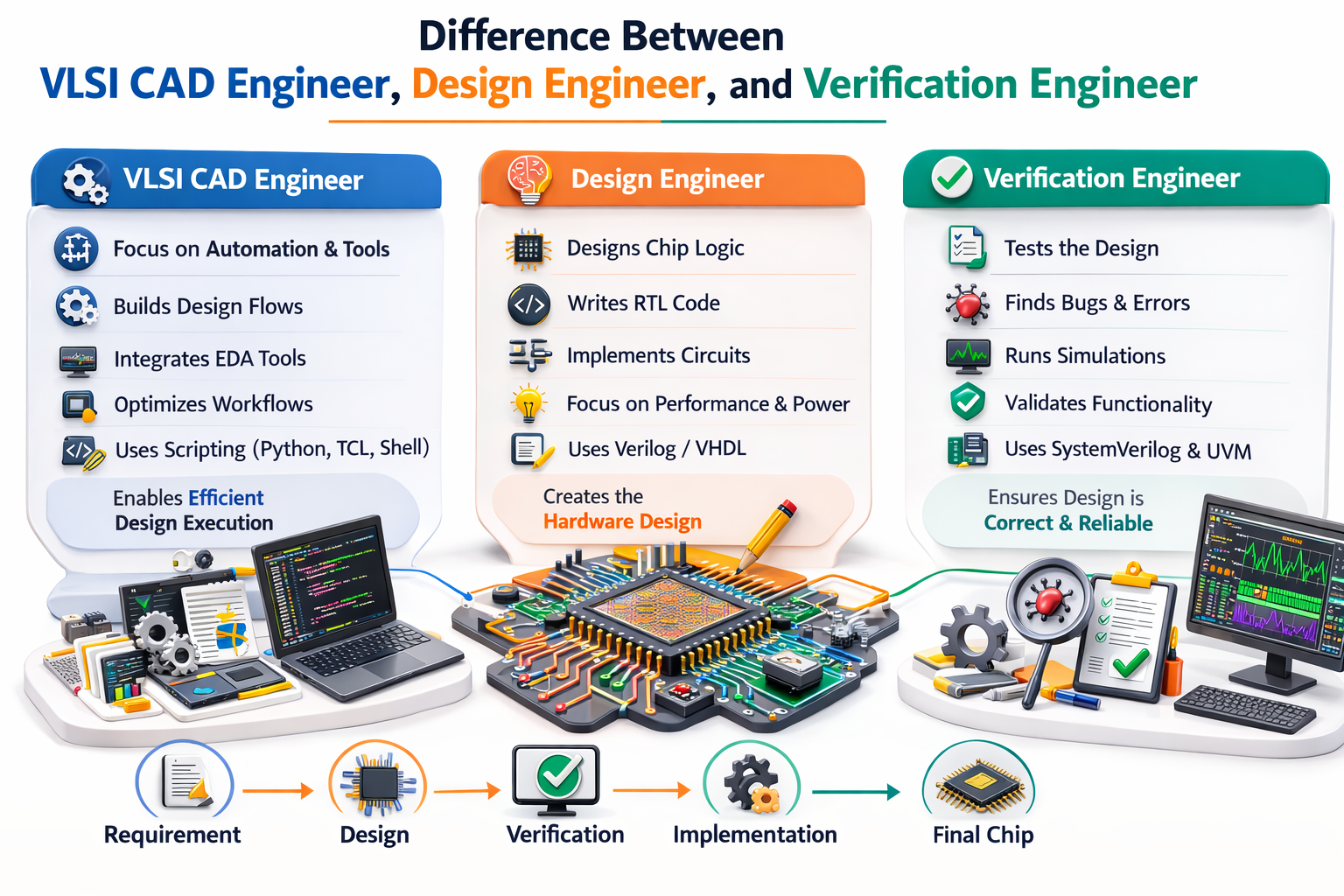
In the semiconductor industry, VLSI CAD engineers, design engineers, and verification engineers perform distinct but closely connected roles within the chip design process. A VLSI design engineer focuses on creating the actual hardware logic of the integrated circuit using hardware description languages such as Verilog or VHDL. Their main responsibility is to convert system-level specifications into RTL (Register Transfer Level) designs that define how the digital circuit will function. Design engineers also optimize logic for performance, power, and area while ensuring that the design meets the required functional and architectural specifications.
A VLSI verification engineer, on the other hand, is responsible for ensuring that the RTL design behaves exactly as intended before it moves to silicon fabrication. Verification engineers develop test environments, write testbenches, and simulate the design to detect bugs and functional errors. They use advanced verification methodologies such as SystemVerilog and UVM (Universal Verification Methodology) along with simulation and debugging tools to validate complex chip designs. Since design errors discovered after fabrication can be extremely costly, verification plays a crucial role in maintaining the quality and reliability of semiconductor products.
A VLSI CAD engineer supports both design and verification teams by managing and optimizing the Electronic Design Automation (EDA) tools and automation flows used throughout the chip development process. Instead of designing or verifying hardware directly, CAD engineers focus on building automated workflows, integrating tools, managing computing environments, and improving design efficiency through scripting and software development. They work closely with design and verification engineers to ensure that the tools used in RTL design, synthesis, simulation, and physical design run smoothly and efficiently, making them an essential part of the modern VLSI development ecosystem.
Best Projects to Build a Strong VLSI CAD Engineer Resume
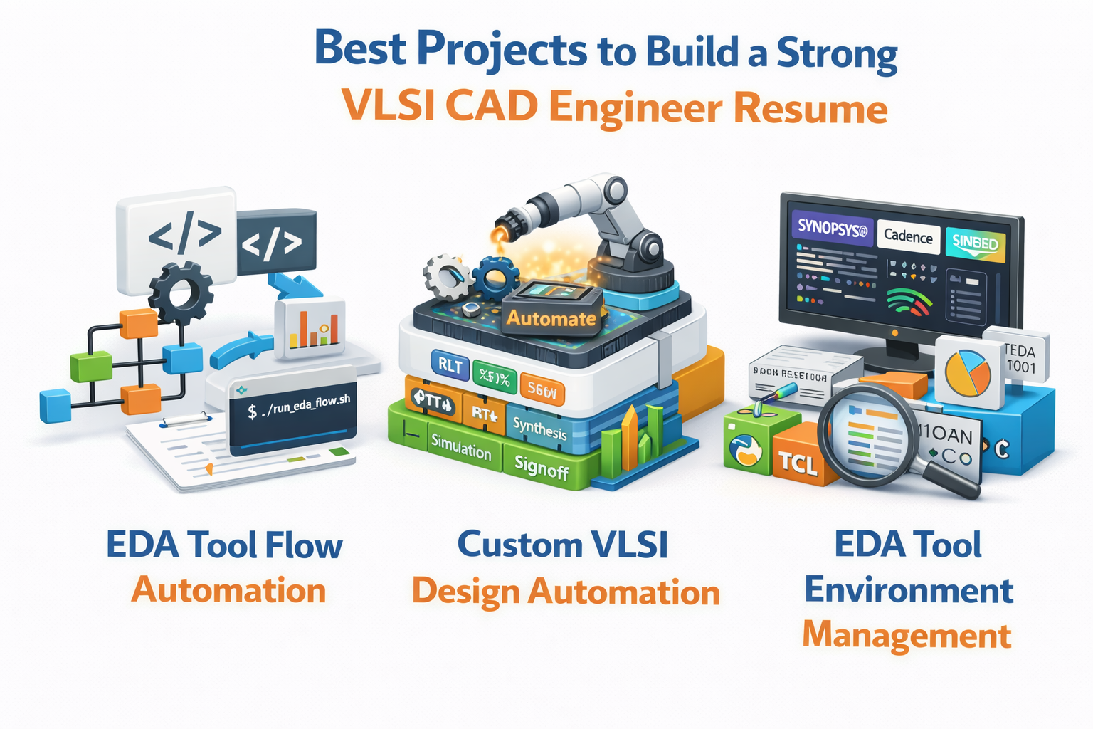
Building strong projects is one of the most effective ways to showcase practical skills required for a VLSI CAD engineer role. Since CAD engineers focus on automation and tool integration, projects related to EDA flow automation and scripting are highly valuable. For example, beginners can create automation scripts using Python, TCL, or Shell scripting to automate tasks such as running synthesis, managing simulation jobs, or organizing design reports. These projects demonstrate the ability to improve design productivity and reduce manual work in the VLSI design environment, which is a key responsibility of CAD engineers in semiconductor companies.
Another valuable project idea is developing a custom VLSI design flow automation framework that integrates multiple stages of the chip design process. This could include automating RTL compilation, simulation, synthesis, and report generation using scripting languages. Such projects help demonstrate an understanding of the complete VLSI design flow and show how automation can connect different EDA tools into a unified workflow. Implementing automation pipelines that run multiple design steps sequentially and generate performance reports can highlight problem-solving skills and practical experience with semiconductor design processes.
In addition, projects focused on EDA tool environment management and data analysis can further strengthen a VLSI CAD engineer resume. For example, candidates can develop scripts that analyze timing reports, optimize design performance metrics, or manage tool environments in a Linux-based system. Creating dashboards or automated report generators for design metrics can also demonstrate strong programming and analytical skills. These types of projects not only show technical expertise but also prove the ability to enhance design efficiency, making them highly attractive to semiconductor companies looking for skilled VLSI CAD engineers.
Future Scope of VLSI CAD Engineering in the Semiconductor Industry

The future scope of VLSI CAD engineering is expanding rapidly as the semiconductor industry continues to evolve with advanced technologies and increasingly complex chip architectures. Modern integrated circuits now contain billions of transistors, and designing these chips efficiently requires highly sophisticated Electronic Design Automation (EDA) tools and automation frameworks. VLSI CAD engineers play a vital role in developing and maintaining these automated design flows, ensuring that engineering teams can handle large-scale System-on-Chip (SoC) designs efficiently. As semiconductor companies move toward advanced technology nodes such as 5nm, 3nm, and beyond, the demand for skilled CAD engineers who can optimize tool performance and automate complex workflows will continue to grow.
Another major factor driving the future of CAD engineering is the integration of Artificial Intelligence (AI) and machine learning into EDA tools. Semiconductor companies are increasingly using AI-driven automation to improve chip design optimization, timing analysis, and layout generation. VLSI CAD engineers are at the forefront of implementing these advanced technologies by developing intelligent automation systems that enhance design productivity and reduce development time. This shift toward AI-assisted chip design will create new opportunities for CAD engineers who possess strong programming, data analysis, and software development skills.
In addition, emerging technologies such as chiplet architectures, heterogeneous integration, and advanced packaging techniques are transforming the semiconductor landscape. These innovations require more sophisticated design environments and improved tool integration, which further increases the importance of CAD engineering expertise. As industries such as AI computing, electric vehicles, 5G communication, and IoT devices continue to demand more powerful and energy-efficient chips, VLSI CAD engineers will remain essential in enabling faster, more reliable semiconductor design processes. This makes CAD engineering a promising and future-proof career path within the global semiconductor industry.
Tips to Start a Career as a VLSI CAD Engineer for Beginners

Starting a career as a VLSI CAD engineer requires a strong combination of semiconductor fundamentals and programming expertise. Beginners should first build a solid understanding of digital electronics, VLSI design flow, and semiconductor fundamentals, as these concepts form the foundation of chip design automation. Learning how the complete design process works—from RTL design and synthesis to verification and physical design—will help aspiring CAD engineers understand where automation and EDA tools are used. Along with theoretical knowledge, beginners should focus on developing strong scripting and programming skills, especially in languages such as Python, TCL, Perl, and Shell scripting, which are widely used for automating design flows and managing tool environments in semiconductor companies.
Another important step is gaining hands-on exposure to EDA tools and Linux-based development environments, since most semiconductor design workflows operate on Linux platforms. Beginners can strengthen their profile by working on projects related to design flow automation, tool integration, and scripting-based workflow optimization. Participating in VLSI training programs, internships, or open-source semiconductor projects can also help build practical experience and industry-relevant skills. By combining technical knowledge, programming expertise, and practical project experience, aspiring engineers can position themselves for rewarding opportunities as VLSI CAD engineers in the rapidly growing semiconductor industry.
Conclusion
The role of a VLSI CAD engineer has become increasingly important in the modern semiconductor industry as chip designs grow more complex and technology continues to advance. By developing and maintaining automation frameworks, integrating EDA tools, and optimizing design workflows, CAD engineers enable design and verification teams to work more efficiently throughout the VLSI design flow. Their expertise in programming, tool management, and design automation helps semiconductor companies accelerate chip development while maintaining high quality and reliability.
As the semiconductor industry expands with innovations in AI computing, electric vehicles, 5G, and advanced SoC architectures, the demand for skilled VLSI CAD engineers is expected to grow significantly. For aspiring engineers, building a strong foundation in VLSI concepts, programming languages, and EDA tools can open the door to exciting career opportunities in this field. With continuous learning and hands-on experience, a career in VLSI CAD engineering offers long-term growth, technical challenges, and the opportunity to contribute to the future of semiconductor technology.