

VLSI Design Fundamentals : Everything You Need to Start a Career in VLSI
Navigate through this article using the table of contents below
Table of Contents
No headings found in this article.
The semiconductor revolution is powering everything from smartphones and AI processors to electric vehicles—and at the heart of this transformation lies VLSI Design. VLSI Design Fundamentals: Everything You Need to Start a Career in VLSI is your gateway to understanding how millions (and even billions) of transistors are integrated onto a single chip. As the global demand for skilled chip designers grows, mastering VLSI (Very Large Scale Integration) has become one of the most promising and high-paying career paths in the electronics and semiconductor industry. Whether you are an engineering student or a working professional aiming to enter chip design, understanding the core principles of semiconductor physics, CMOS technology, and digital circuit design is the first crucial step.
This comprehensive guide explores the essential building blocks of VLSI design, including CMOS logic design, hardware description languages (HDL) such as Verilog and VHDL, VLSI design flow, physical design, verification, and fabrication processes. You will gain insights into front-end and back-end design methodologies, EDA tools, and industry-relevant skills required to secure a job in top semiconductor companies. By building a strong foundation in VLSI fundamentals, you position yourself for career opportunities in chip design, FPGA development, ASIC design, and semiconductor research—making this field a future-proof choice in today’s technology-driven world.
Introduction to VLSI Design and the Semiconductor Industry
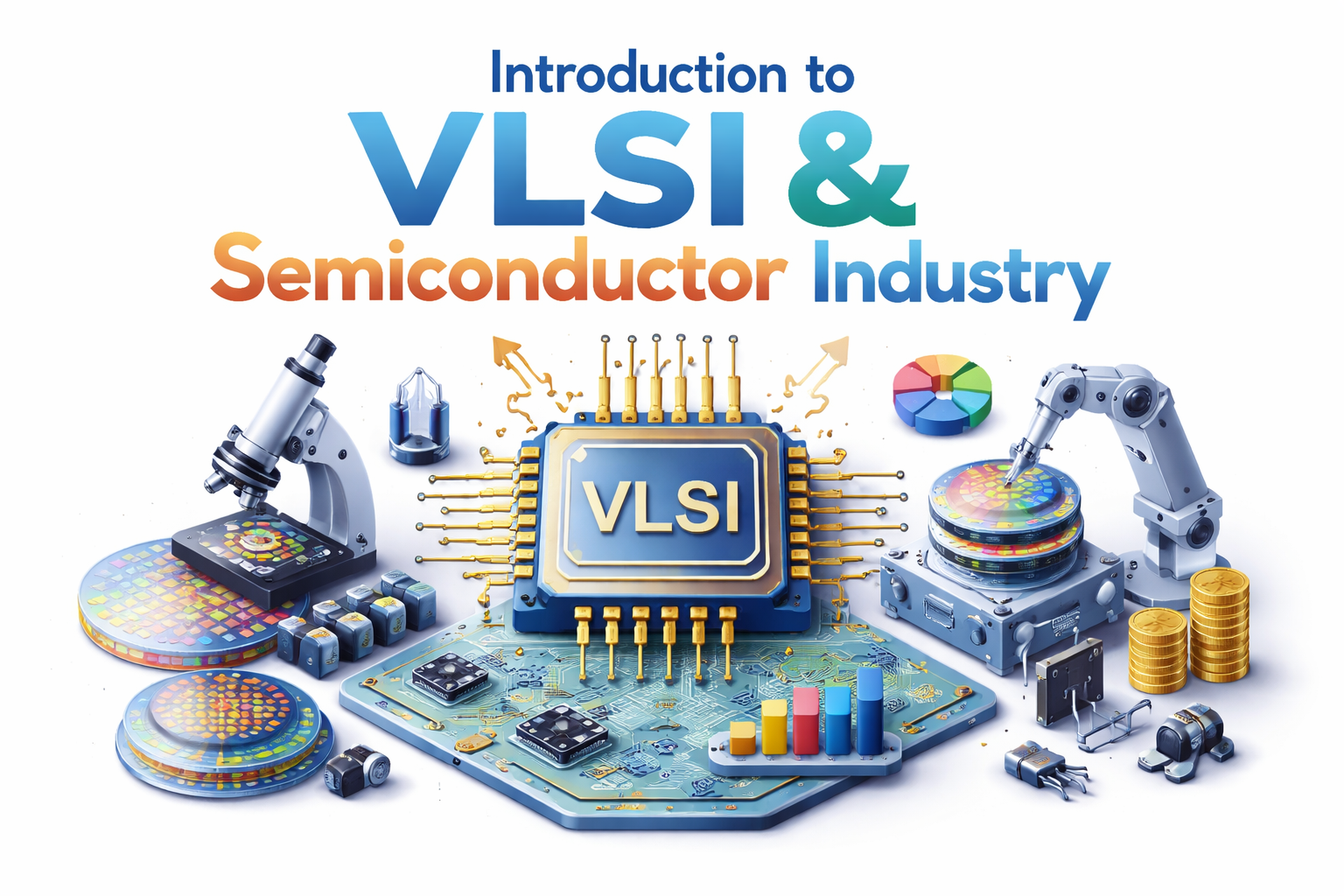
Very Large Scale Integration (VLSI) design is the process of integrating millions to billions of transistors onto a single silicon chip to create complex integrated circuits (ICs). From microprocessors and memory chips to system-on-chip (SoC) architectures, VLSI technology forms the backbone of modern electronics. The evolution of integrated circuits—from Small-Scale Integration (SSI) to Ultra-Large-Scale Integration (ULSI)—has enabled powerful computing devices, artificial intelligence accelerators, and high-speed communication systems. At the core of VLSI lies CMOS (Complementary Metal-Oxide-Semiconductor) technology, which offers high performance with low power consumption, making it the industry standard for chip fabrication. Understanding VLSI design fundamentals is essential for engineers aiming to build scalable, efficient, and high-speed semiconductor solutions.
The global semiconductor industry has experienced rapid growth due to increasing demand for smartphones, electric vehicles, IoT devices, and data centers. Leading semiconductor companies such as Intel, TSMC, and Samsung Electronics are driving innovation in advanced process nodes and chip manufacturing technologies. With nations investing heavily in semiconductor ecosystems, the demand for skilled VLSI engineers in areas like RTL design, physical design, verification, and chip testing continues to rise. As digital transformation accelerates worldwide, VLSI design remains one of the most promising and future-proof career paths within the semiconductor industry.
Basics of Semiconductor Physics

Semiconductor physics forms the theoretical foundation of VLSI design, enabling engineers to understand how electronic devices operate at the atomic and carrier-transport level. Semiconductors such as silicon exhibit electrical conductivity between conductors and insulators, which can be precisely controlled through doping. Intrinsic semiconductors become extrinsic when doped with pentavalent (n-type) or trivalent (p-type) impurities, creating free electrons and holes as charge carriers. The formation of a PN junction—by joining p-type and n-type materials—leads to the creation of a depletion region and built-in potential, which is fundamental to diode and transistor operation. Mastery of energy band theory, carrier mobility, drift and diffusion mechanisms, and recombination processes is essential for analyzing device behavior in integrated circuits.
For VLSI engineers, the most critical device derived from semiconductor physics is the MOSFET (Metal-Oxide-Semiconductor Field-Effect Transistor), the building block of CMOS technology. The operation of a MOSFET depends on threshold voltage, channel formation, oxide capacitance, and current-voltage (I–V) characteristics. Parameters such as leakage current, short-channel effects, and scaling limitations directly influence power consumption, switching speed, and overall chip performance. A strong understanding of these physical principles allows engineers to design low-power, high-speed circuits and optimize transistor-level implementations in advanced semiconductor nodes. In modern VLSI systems, semiconductor physics is not merely theoretical—it directly impacts reliability, efficiency, and manufacturability of integrated circuits.
CMOS Technology and CMOS Logic Design

Complementary Metal-Oxide-Semiconductor (CMOS) technology is the dominant fabrication technology used in modern VLSI design due to its low power consumption, high noise immunity, and scalability. CMOS circuits are built using complementary pairs of p-type MOS (PMOS) and n-type MOS (NMOS) transistors, which work together to achieve efficient switching behavior. Unlike earlier logic families, CMOS significantly reduces static power dissipation because current flows only during switching transitions. This makes CMOS ideal for high-density integrated circuits such as microprocessors, memory chips, and system-on-chip (SoC) devices. The scalability of CMOS technology has enabled the semiconductor industry to follow Moore’s Law, integrating billions of transistors on a single silicon die while maintaining performance efficiency.
At the core of CMOS logic design is the CMOS inverter, the fundamental building block of digital circuits. A CMOS inverter consists of one PMOS transistor connected to VDD (power supply) and one NMOS transistor connected to ground. When the input is low, the PMOS conducts and the NMOS turns off, producing a high output; when the input is high, the NMOS conducts and the PMOS turns off, producing a low output. This complementary switching mechanism ensures minimal static power consumption and strong logic levels. Building upon the inverter, engineers design complex combinational logic gates such as NAND, NOR, XOR, and sequential elements like flip-flops and registers, forming the basis of digital integrated circuit design.
In advanced VLSI systems, CMOS logic design must consider critical performance parameters such as propagation delay, dynamic power dissipation, leakage currents, and noise margins. Power consumption in CMOS circuits is primarily dynamic, driven by switching activity, capacitive load, and supply voltage. As device dimensions shrink in deep submicron technologies, challenges such as short-channel effects, threshold voltage variations, and increased leakage current become significant design constraints. Therefore, modern CMOS design techniques focus on low-power optimization, transistor sizing, clock gating, and multi-threshold voltage strategies. A solid understanding of CMOS technology and logic design principles enables VLSI engineers to develop energy-efficient, high-performance semiconductor chips for next-generation applications.
Digital Electronics Fundamentals for VLSI
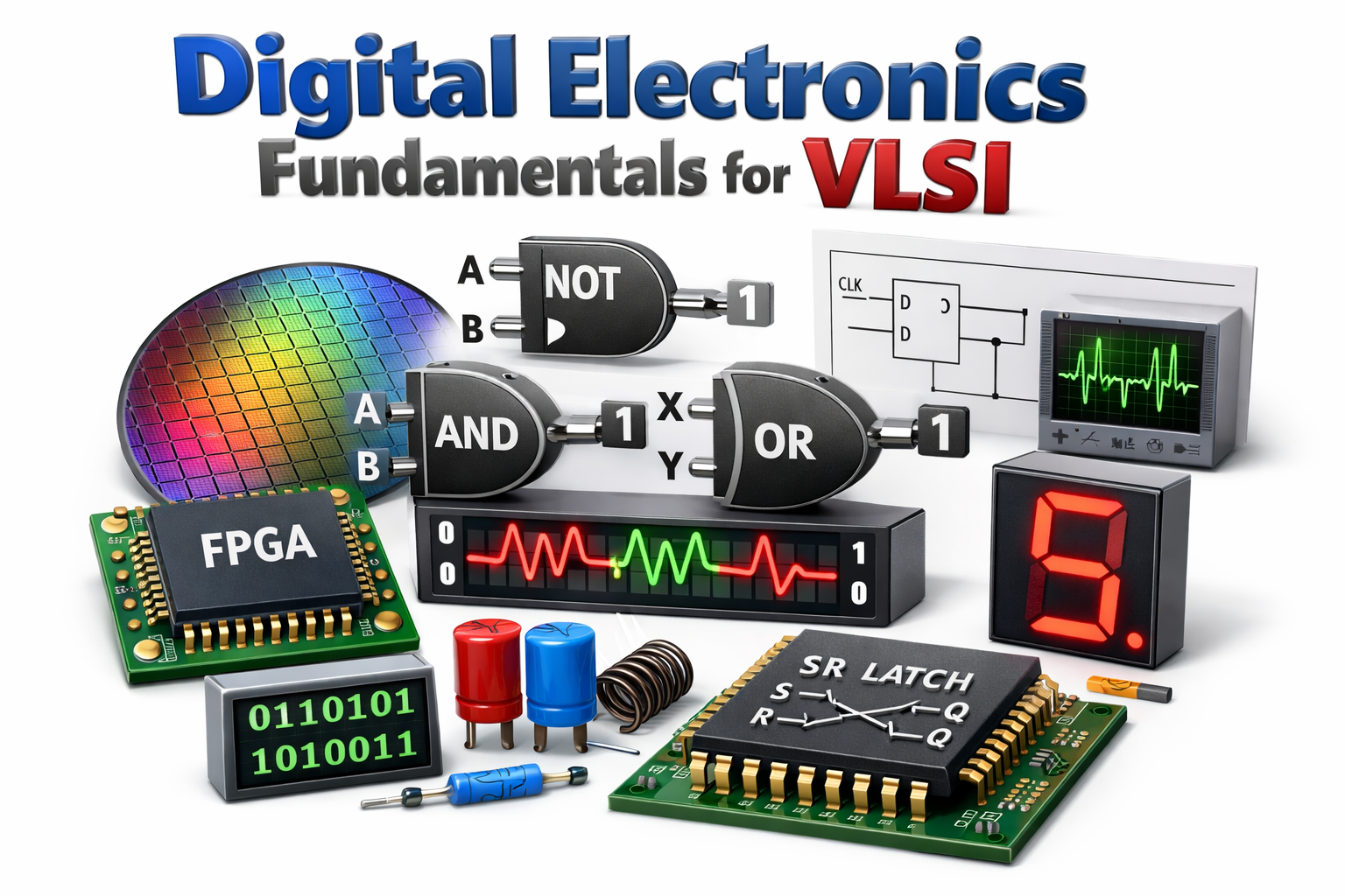
Digital electronics is the backbone of VLSI design, providing the logical and architectural framework required to build integrated circuits. At its core, digital design is based on binary logic, Boolean algebra, and logic gates such as AND, OR, NOT, NAND, and NOR. These gates are combined to form combinational circuits, where outputs depend solely on present inputs, and sequential circuits, where outputs depend on both current inputs and past states. Key building blocks such as multiplexers, decoders, adders, flip-flops, registers, and counters form the foundation of complex digital systems including microprocessors and memory units. A strong understanding of logic minimization techniques, Karnaugh maps (K-maps), and finite state machines (FSMs) is essential for designing optimized and area-efficient VLSI circuits.
In practical VLSI implementation, timing analysis and clocking concepts play a critical role in ensuring reliable circuit operation. Parameters such as propagation delay, setup time, hold time, clock skew, and metastability directly impact performance and stability. Synchronous design methodology, which relies on clock-driven sequential elements, is widely adopted in modern chip design to maintain predictable timing behavior. Engineers must also understand hazards, glitches, and race conditions to prevent functional errors in high-speed circuits. Mastery of digital electronics fundamentals enables VLSI engineers to design scalable, high-performance, and timing-accurate integrated circuits suitable for ASIC and FPGA development. To master core concepts like logic gates, circuits, and CMOS design, you should explore a detailed Analog & Digital Electronics course.
Complete VLSI Design Flow (Front-End to Back-End)
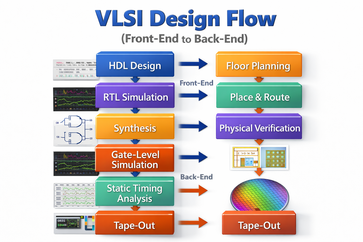
The VLSI design flow is a structured, multi-stage process that transforms a system specification into a manufacturable integrated circuit. It begins with requirement analysis and architectural design, where system-level functionality, performance targets, power budgets, and area constraints are defined. This is followed by RTL (Register Transfer Level) design using hardware description languages such as Verilog or VHDL. Functional verification ensures that the RTL code meets design specifications through simulation and testbenches. Once verified, the RTL is synthesized into a gate-level netlist using standard cell libraries, optimizing for timing, power, and area constraints. This phase, commonly referred to as the front-end design flow, focuses on logical correctness and design intent.
After synthesis, the process transitions into the back-end or physical design flow, where the logical netlist is transformed into a physical layout. Key stages include floorplanning, power planning, placement of standard cells, clock tree synthesis (CTS), and routing of interconnections. Engineers perform static timing analysis (STA) to verify timing closure and ensure that setup and hold requirements are met across all process, voltage, and temperature (PVT) corners. Additional checks such as signal integrity analysis, electromigration (EM) analysis, and IR drop analysis are conducted to guarantee reliability. Design for Testability (DFT) structures are also inserted to facilitate post-fabrication testing.
The final stage involves physical verification processes such as Design Rule Check (DRC), Layout Versus Schematic (LVS), and parasitic extraction to ensure manufacturability and accuracy. Once all checks are cleared, the design proceeds to tape-out, where the layout data is sent to the semiconductor foundry for fabrication. Throughout the entire VLSI design flow, Electronic Design Automation (EDA) tools play a critical role in automating complex tasks and ensuring precision. A comprehensive understanding of both front-end and back-end VLSI design processes enables engineers to develop high-performance, low-power ASIC and SoC solutions ready for silicon implementation.
VLSI Verification and Testing Fundamentals

VLSI verification is a critical phase in the chip design lifecycle that ensures the functional correctness and reliability of an integrated circuit before fabrication. Since manufacturing errors are extremely costly, verification aims to identify and eliminate logical, timing, and structural bugs at early stages. The process begins at the RTL level with functional verification, where simulation-based methodologies and testbenches validate that the design behaves according to its specifications. Advanced verification techniques include constrained random testing, assertion-based verification, and coverage-driven verification to measure test completeness. Static Timing Analysis (STA) is performed after synthesis and during physical design to ensure that setup and hold time requirements are satisfied under different process, voltage, and temperature (PVT) conditions. A robust verification strategy significantly reduces silicon re-spins and enhances first-time-right success rates.
In addition to functional verification, VLSI testing focuses on detecting manufacturing defects after chip fabrication. Design for Testability (DFT) techniques such as scan chains, Built-In Self-Test (BIST), and boundary scan are integrated into the design to improve fault coverage. Fault models, including stuck-at faults and transition faults, are used to generate Automatic Test Pattern Generation (ATPG) vectors that validate chip functionality. Post-silicon validation and testing ensure that the fabricated IC meets performance, power, and reliability standards. As technology nodes shrink and circuit complexity increases, verification and testing account for a major portion of the overall design effort, making expertise in this domain highly valuable for VLSI engineers working in ASIC and SoC development.
Skills Required to Start a Career in VLSI
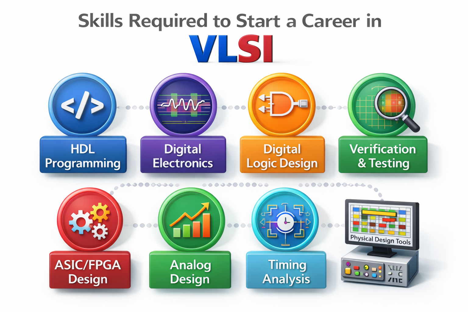
Building a successful career in VLSI requires a strong foundation in core electronics and semiconductor concepts. Engineers must thoroughly understand digital electronics, CMOS technology, semiconductor physics, and VLSI design flow. Proficiency in combinational and sequential circuit design, timing analysis, and low-power design techniques is essential. A clear grasp of concepts such as setup and hold time, clock domains, propagation delay, and power optimization strategies directly impacts performance and reliability in chip design. Additionally, understanding both front-end (RTL design and verification) and back-end (physical design and timing closure) domains provides a competitive advantage in the semiconductor industry.
To build these skills in a structured and industry-focused way, many aspiring engineers choose platforms like JastTech, which offer practical training aligned with real-world semiconductor workflows and tools. Technical tool proficiency is equally critical for aspiring VLSI engineers. Hands-on experience with Hardware Description Languages (HDL) such as Verilog or VHDL is mandatory for RTL development. Knowledge of simulation, synthesis, and verification methodologies strengthens employability. Familiarity with industry-standard EDA tools from companies like Cadence Design Systems and Synopsys enhances practical capability in ASIC and SoC development. For verification roles, understanding SystemVerilog and scripting languages such as Python or TCL is beneficial. Exposure to FPGA prototyping and real-time hardware debugging further strengthens technical competence.
Beyond technical expertise, analytical thinking, problem-solving ability, and attention to detail are indispensable skills in VLSI engineering. Since chip design involves complex architectures and tight performance constraints, engineers must be capable of debugging intricate timing violations and optimizing power-performance-area (PPA) metrics. Strong mathematical aptitude, particularly in Boolean algebra and signal processing fundamentals, supports design efficiency. Participation in internships, academic projects, and industry-relevant certifications significantly improves job readiness. A combination of theoretical depth, tool proficiency, and practical implementation skills forms the foundation for launching a successful career in the VLSI domain.
Top Job Roles in VLSI Industry
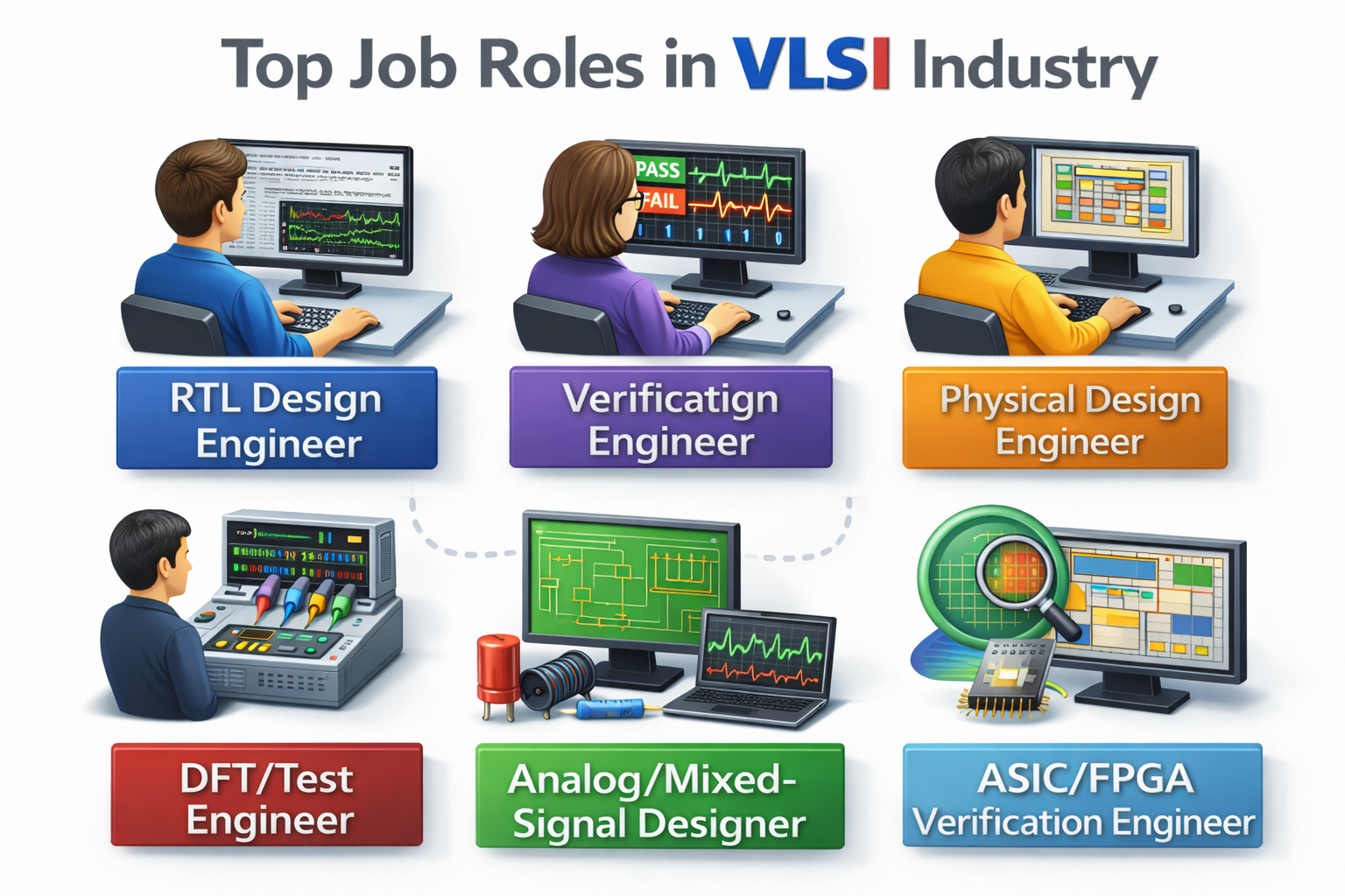
The VLSI industry offers diverse and specialized job roles across the front-end and back-end design spectrum. One of the most prominent roles is the RTL Design Engineer, who develops and optimizes hardware logic using HDL languages such as Verilog or VHDL based on architectural specifications. Verification Engineers play a crucial role in ensuring functional correctness through simulation, testbench development, and coverage-driven methodologies, often using SystemVerilog and UVM. On the back-end side, Physical Design Engineers handle floorplanning, placement, clock tree synthesis (CTS), routing, and timing closure to convert logical designs into manufacturable layouts. Each of these roles requires strong expertise in digital design concepts, timing analysis, and power-performance-area (PPA) optimization.
In addition to core design roles, specialized positions such as DFT (Design for Test) Engineer, STA (Static Timing Analysis) Engineer, and FPGA Design Engineer are in high demand within the semiconductor ecosystem. DFT engineers integrate scan chains and test structures to ensure high fault coverage in manufactured chips, while STA engineers focus on timing verification across multiple process, voltage, and temperature (PVT) conditions. FPGA engineers work on configurable hardware platforms for rapid prototyping and embedded systems development. As semiconductor companies continue to innovate in ASIC and SoC technologies, these VLSI job roles offer strong career growth, competitive salaries, and opportunities to work on cutting-edge chip design projects.
Salary Trends and Future Scope of VLSI in India and Globally

The VLSI industry has become one of the most lucrative sectors for engineering professionals, driven by rapid advancements in semiconductor technology and widespread adoption of digital systems. In India, entry-level VLSI engineers typically command competitive starting salaries compared with traditional electronics roles, with compensation packages influenced by skills in hardware description languages (HDL), verification methodologies, and EDA tools. As engineers gain experience—particularly in RTL design, physical design, or verification—their earning potential increases significantly. Mid-level and senior engineers with specialized expertise in areas like static timing analysis (STA), low-power design, or advanced process nodes often secure higher remuneration, reflecting the growing demand for skilled talent in both domestic and multinational semiconductor firms.
Globally, the salary trends for VLSI professionals reflect the strategic importance of semiconductor design across industries such as consumer electronics, automotive, telecommunications, and cloud computing infrastructure. In major semiconductor hubs such as the United States, Taiwan, South Korea, and Europe, experienced VLSI engineers often receive premium compensation packages, including performance bonuses and equity, especially in roles that involve complex system-on-chip (SoC) development or leadership of design teams. Demand for expertise in emerging technologies—such as AI accelerators, 5G chipsets, and heterogeneous computing architectures—continues to push salaries higher, particularly for specialized roles in verification, physical design, and design automation.
The future scope of VLSI remains robust, fueled by global investments in semiconductor manufacturing, research initiatives, and government policies aimed at reducing dependence on external supply chains. In India, initiatives such as semiconductor manufacturing plants and skill development programs are expected to strengthen the local ecosystem and create more high-value engineering jobs. With the proliferation of Internet of Things (IoT), autonomous vehicles, wearable technology, and next-generation communication systems, the demand for VLSI engineers is projected to grow exponentially. As chip designs become more complex and process technologies advance into sub-nanometer nodes, opportunities for innovation, high earnings, and career growth in VLSI will continue to expand both in India and internationally.
Step-by-Step Roadmap to Become a VLSI Engineer
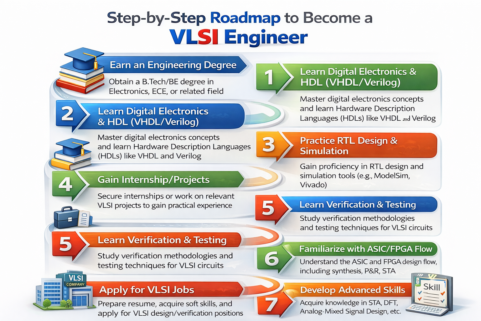
Becoming a VLSI engineer requires a structured learning path that begins with building strong fundamentals in electronics and semiconductor concepts. The first step is mastering digital electronics, Boolean algebra, CMOS logic design, and semiconductor physics. A clear understanding of combinational and sequential circuits, timing analysis, and low-power design principles forms the technical base for chip design. The next stage involves learning Hardware Description Languages (HDL) such as Verilog or VHDL to design and simulate RTL-level circuits. Simultaneously, gaining familiarity with the complete VLSI design flow—from specification and synthesis to physical design and verification—helps develop a holistic understanding of ASIC and SoC development processes.
After establishing core knowledge, practical exposure becomes critical. Engineers should work on mini-projects such as designing an ALU, FIFO, or simple processor module using RTL coding and simulation tools. Learning verification methodologies, static timing analysis (STA), and basic scripting (Python or TCL) enhances employability. For those interested in specialization, choosing a focused domain—RTL design, verification, physical design, or DFT—provides a clear career direction. Internships, industry-oriented training programs, and certifications strengthen professional credibility. Continuous learning, hands-on tool experience, and problem-solving ability are essential to successfully transition from an electronics graduate to a skilled VLSI engineer in the competitive semiconductor industry.
Conclusion
VLSI design stands at the core of modern technological innovation, powering everything from smartphones and data centers to automotive electronics and AI-driven systems. By understanding semiconductor physics, CMOS technology, digital electronics, HDL programming, verification methodologies, and the complete VLSI design flow, aspiring engineers can build a strong technical foundation for a successful career in the semiconductor industry. The field demands precision, analytical thinking, and continuous skill development, but it also offers high-growth opportunities, competitive salaries, and the chance to contribute to cutting-edge chip design advancements.
As global demand for advanced integrated circuits continues to rise, the future of VLSI remains exceptionally promising, especially in emerging areas such as low-power design, AI accelerators, and next-generation communication systems. With the right roadmap—strong fundamentals, hands-on project experience, tool proficiency, and domain specialization—any dedicated learner can transition into a professional VLSI engineer. Investing time in mastering VLSI fundamentals today not only ensures career stability but also positions you at the forefront of the rapidly evolving semiconductor ecosystem.