

VLSI DFT and Test Engineer Roles: Key Skills and Job Outlook
Navigate through this article using the table of contents below
Table of Contents
No headings found in this article.
The semiconductor industry is rapidly evolving, and ensuring that complex chips function correctly before they reach the market is more critical than ever. This is where VLSI DFT (Design for Testability) and Test Engineers play a crucial role. As modern integrated circuits become more advanced and densely packed with billions of transistors, verifying their reliability and detecting manufacturing defects has become a specialized engineering discipline. VLSI DFT and Test Engineers focus on building efficient testing architectures such as scan chains, boundary scan, and Automatic Test Pattern Generation (ATPG) to ensure that chips can be thoroughly tested during manufacturing and post-silicon validation.
With the global demand for semiconductors rising across industries like artificial intelligence, automotive electronics, consumer devices, and telecommunications, the need for skilled VLSI DFT and Test Engineers is also growing significantly. These professionals work closely with design, verification, and physical design teams to integrate test logic into chip designs, improving fault coverage and reducing production costs. In this article, we will explore the roles and responsibilities of VLSI DFT and Test Engineers, the key skills required for this career path, and the future job outlook in the semiconductor industry, helping aspiring engineers understand how to build a successful career in this high-demand VLSI domain.
Introduction to VLSI DFT (Design for Testability) and Chip Testing
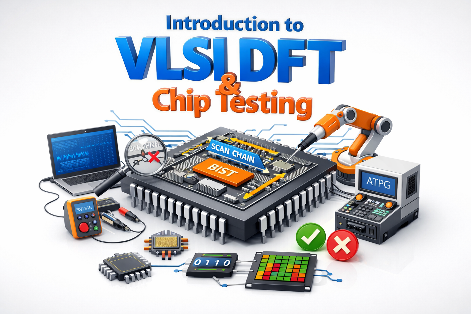
VLSI DFT (Design for Testability) is a crucial methodology used in semiconductor design to ensure that integrated circuits (ICs) can be efficiently tested for manufacturing defects and functional errors. As modern chips become more complex, containing billions of transistors, verifying their reliability and correctness before mass production becomes increasingly challenging. DFT techniques are incorporated into the chip design during the early stages of the VLSI design flow, allowing engineers to simplify the testing process and detect faults such as stuck-at faults, delay faults, and bridging faults. By embedding special test logic inside the design, engineers can improve test coverage and ensure that defective chips are identified before reaching the market.
Chip testing plays a vital role in maintaining the quality, reliability, and performance of semiconductor devices used in applications such as smartphones, automotive electronics, AI processors, and IoT systems. VLSI test engineers use various DFT techniques like Scan Chains, Boundary Scan (JTAG), Built-In Self-Test (BIST), and Automatic Test Pattern Generation (ATPG) to detect faults and validate chip functionality during manufacturing and post-silicon testing. These techniques help reduce production costs, increase manufacturing yield, and ensure that only fully functional chips are delivered to customers, making DFT an essential part of modern semiconductor development.
Importance of Testing in the VLSI Design Flow

Testing is a critical stage in the VLSI design flow because it ensures that integrated circuits (ICs) function correctly after manufacturing. Modern semiconductor chips contain millions or even billions of transistors, making them highly complex systems where even a small defect can lead to functional failure. During fabrication, imperfections such as open connections, short circuits, or timing issues can occur. VLSI testing helps identify these defects early by using structured testing techniques, allowing manufacturers to detect faulty chips before they reach the market. This process is essential for maintaining the quality and reliability of semiconductor devices used in consumer electronics, automotive systems, and communication technologies.
Another important reason for testing in the VLSI design flow is to improve manufacturing yield and reduce production costs. Without proper testing mechanisms, defective chips may pass through the manufacturing process and lead to costly product recalls or system failures in real-world applications. Design for Testability (DFT) techniques such as scan insertion, boundary scan, and Automatic Test Pattern Generation (ATPG) enable engineers to thoroughly verify chip functionality and detect faults efficiently. These techniques allow engineers to apply specific test patterns to the circuit and analyze the output responses, ensuring that the chip behaves according to its design specifications.
Testing also plays a significant role in ensuring the long-term reliability and performance of semiconductor devices. As chips are used in critical applications such as aerospace systems, medical devices, and autonomous vehicles, their reliability becomes extremely important. By incorporating robust testing strategies throughout the VLSI design and manufacturing process, engineers can verify the functionality, timing behavior, and fault tolerance of the chip. This not only increases confidence in the product but also strengthens the reputation of semiconductor companies by delivering high-quality and dependable electronic components.
What Does a VLSI DFT Engineer Do? Roles and Responsibilities
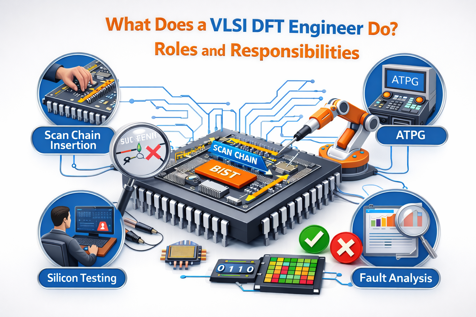
A VLSI DFT (Design for Testability) Engineer is responsible for designing and implementing test structures within integrated circuits to ensure that chips can be efficiently tested for manufacturing defects and functional issues. During the chip design process, DFT engineers add specialized test logic such as scan chains, boundary scan (JTAG), Built-In Self-Test (BIST), and memory BIST (MBIST) to make the design more testable. They work closely with RTL design, verification, and physical design teams to integrate these test features without affecting the overall performance, area, or power consumption of the chip. Their main objective is to improve fault detection and test coverage so that defective chips can be identified during manufacturing.
In addition to implementing test architectures, VLSI DFT engineers are also responsible for generating and analyzing test patterns using Automatic Test Pattern Generation (ATPG) tools, performing fault simulations, and debugging test failures. They analyze fault coverage reports, optimize scan chain configurations, and ensure that the design meets industry testing standards before tape-out. DFT engineers also collaborate with manufacturing test teams to support silicon validation and production testing. By ensuring that chips are thoroughly testable and reliable, VLSI DFT engineers play a critical role in delivering high-quality semiconductor products used in modern electronics, automotive systems, and advanced computing technologies.
Key Skills Required to Become a VLSI DFT and Test Engineer
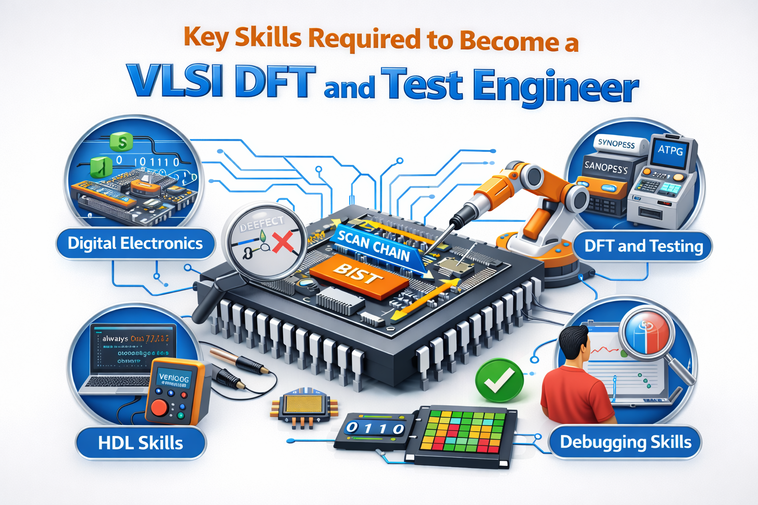
To become a successful VLSI DFT and Test Engineer, a strong understanding of digital electronics and VLSI design fundamentals is essential. Engineers must be familiar with concepts such as combinational and sequential circuits, finite state machines, timing analysis, and RTL design. Knowledge of hardware description languages like Verilog or VHDL is also important because DFT logic is often integrated into the design at the RTL or gate level. In addition, a solid grasp of fault models such as stuck-at faults, transition faults, and bridging faults helps engineers understand how defects occur in integrated circuits and how they can be detected through testing techniques.
Another important skill is expertise in DFT methodologies and testing techniques used in modern semiconductor design. VLSI DFT engineers must understand concepts such as scan chain insertion, boundary scan (JTAG), Built-In Self-Test (BIST), Memory BIST (MBIST), and Automatic Test Pattern Generation (ATPG). These techniques allow engineers to create efficient test structures and generate patterns that help identify defects in the chip during manufacturing. Familiarity with industry-standard EDA tools such as Synopsys DFT Compiler, Mentor Tessent, and Cadence Modus is also highly valuable, as these tools are widely used for implementing DFT architectures and analyzing test coverage.
In addition to technical expertise, problem-solving ability and debugging skills are crucial for a VLSI DFT engineer. Engineers often analyze test failures, review fault coverage reports, and work with design and verification teams to identify the root causes of defects. Strong analytical thinking, attention to detail, and the ability to collaborate across multiple engineering teams are essential for success in this field. As semiconductor technology continues to evolve with advanced nodes and complex chip architectures, engineers who continuously upgrade their knowledge of testing methodologies and tools will have strong career opportunities in the VLSI and semiconductor industry.
Difference Between DFT Engineer, Verification Engineer, and Physical Design Engineer
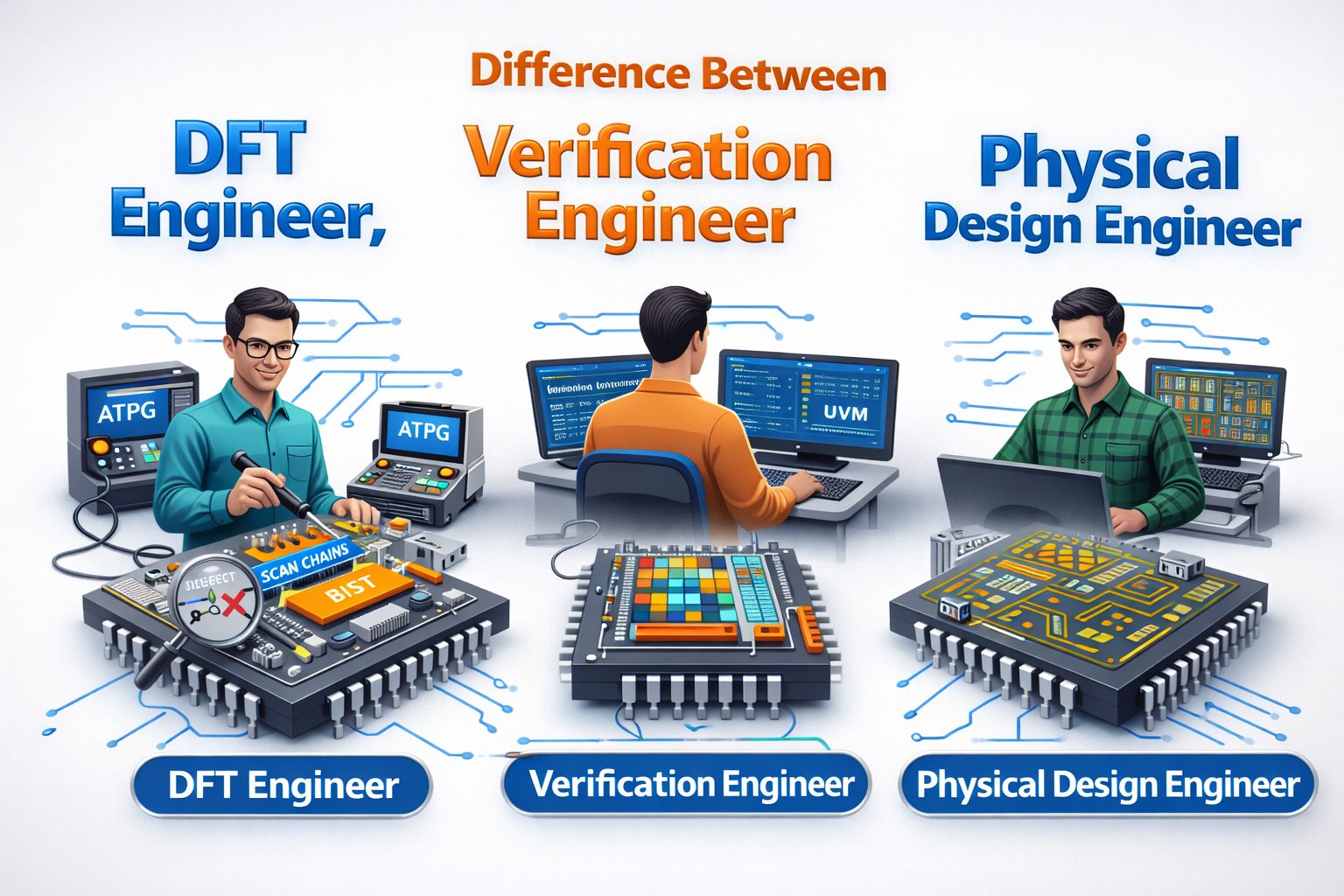
In the VLSI industry, DFT Engineers, Verification Engineers, and Physical Design Engineers play distinct but interconnected roles in the chip development process. A DFT (Design for Testability) Engineer focuses on making integrated circuits easier to test during manufacturing by inserting test structures such as scan chains, boundary scan (JTAG), and Built-In Self-Test (BIST). Their primary responsibility is to ensure high fault coverage and enable efficient chip testing using techniques like Automatic Test Pattern Generation (ATPG). In contrast, a Verification Engineer is responsible for verifying that the RTL design functions correctly according to the design specifications. They use simulation, testbenches, and verification methodologies such as SystemVerilog and UVM to detect functional bugs before the chip moves to the manufacturing stage.
A Physical Design Engineer, on the other hand, works on the backend of the VLSI design flow and focuses on converting the logical design into a physical layout that can be manufactured on silicon. Their responsibilities include floorplanning, placement, clock tree synthesis, routing, and timing closure while ensuring the chip meets power, performance, and area constraints. While verification engineers ensure the design works logically and DFT engineers ensure it can be effectively tested, physical design engineers ensure the chip can be physically fabricated with optimal performance. Together, these roles form a critical part of the semiconductor design process, ensuring that modern integrated circuits are functional, testable, and manufacturable.
Career Path of a VLSI DFT Engineer (Entry-Level to Senior Roles)

The career path of a VLSI DFT (Design for Testability) Engineer typically begins with entry-level roles where engineers focus on learning the fundamentals of semiconductor testing and design-for-test techniques. As a Junior DFT Engineer or DFT Engineer, professionals work on tasks such as scan chain insertion, running Automatic Test Pattern Generation (ATPG), analyzing fault coverage reports, and assisting senior engineers in debugging test issues. At this stage, engineers also gain hands-on experience with industry-standard EDA tools like Synopsys DFT Compiler, Mentor Tessent, and Cadence Modus, while strengthening their knowledge of digital design, fault models, and chip testing methodologies.
With a few years of industry experience, engineers progress to roles such as Senior DFT Engineer or Lead DFT Engineer, where they take on more complex responsibilities. These may include designing advanced test architectures, implementing Memory BIST (MBIST) and Logic BIST (LBIST) solutions, optimizing scan chains for better test coverage, and collaborating closely with RTL, verification, and physical design teams. Senior engineers also play a key role in debugging silicon test failures, improving manufacturing yield, and ensuring that the chip meets testing requirements before tape-out. Leadership and mentoring responsibilities often begin at this stage, as experienced engineers guide junior team members.
At advanced stages of the career, professionals may move into positions such as DFT Architect, Test Engineering Manager, or Semiconductor Technical Lead. In these roles, engineers are responsible for defining the overall test strategy for complex System-on-Chip (SoC) designs, evaluating new testing technologies, and ensuring compliance with industry standards. They also contribute to strategic decisions related to chip reliability, production testing, and cost optimization. With the continuous growth of semiconductor technologies and applications in AI, automotive electronics, and high-performance computing, experienced VLSI DFT engineers have strong opportunities for career advancement and leadership roles in the semiconductor industry.
Future Scope of DFT and Semiconductor Testing Careers

The future scope of DFT (Design for Testability) and semiconductor testing careers is expanding rapidly as modern chips become more complex and are used in a wide range of advanced technologies. With the growth of industries such as artificial intelligence, 5G communication, electric vehicles, IoT devices, and high-performance computing, semiconductor companies are designing increasingly sophisticated integrated circuits containing billions of transistors. Ensuring that these chips are reliable and free from manufacturing defects requires advanced testing techniques and highly skilled DFT engineers. As a result, professionals specializing in scan architecture, ATPG, BIST, and fault analysis are expected to remain in high demand across global semiconductor companies.
In addition, emerging semiconductor technologies such as advanced process nodes, 3D ICs, chiplet-based architectures, and system-on-chip (SoC) designs are making chip testing more challenging and technically demanding. This is driving the need for innovative DFT methodologies, automated testing tools, and engineers who can develop efficient test strategies for complex designs. With semiconductor manufacturing expanding globally and governments investing heavily in chip production, career opportunities for VLSI DFT and Test Engineers are expected to grow significantly. Engineers who continuously upgrade their skills in testing techniques, EDA tools, and semiconductor design concepts will have strong long-term career prospects in the semiconductor industry.
Tips for Beginners to Start a Career in VLSI DFT Engineering
Starting a career in VLSI DFT (Design for Testability) engineering requires a strong foundation in digital electronics and VLSI design concepts. Beginners should first focus on understanding core topics such as combinational and sequential logic, finite state machines, and the basics of the VLSI design flow. Learning hardware description languages like Verilog or VHDL is essential because most chip designs are described using these languages. In addition, gaining knowledge of fault models such as stuck-at faults, transition faults, and bridging faults helps beginners understand how defects occur in integrated circuits and how they can be detected during testing.
Another important step for beginners is to learn the fundamental DFT techniques used in semiconductor testing. Concepts such as scan chain insertion, boundary scan (JTAG), Built-In Self-Test (BIST), Memory BIST (MBIST), and Automatic Test Pattern Generation (ATPG) are widely used in the industry to improve chip testability. Beginners should also try to gain hands-on exposure to EDA tools commonly used by DFT engineers, including Synopsys DFT Compiler, Mentor Tessent, and Cadence Modus. Practical learning through online courses, VLSI training programs, and small design projects can help build confidence and industry-ready skills.
Finally, beginners should focus on building a strong portfolio and staying updated with the latest trends in the semiconductor industry. Working on DFT-related projects, participating in internships, and learning debugging techniques for scan and ATPG failures can significantly improve job readiness. Networking with professionals, attending semiconductor webinars, and following industry developments can also help beginners understand current market demands. With consistent practice, continuous learning, and hands-on experience, aspiring engineers can successfully build a rewarding career in VLSI DFT and semiconductor testing.
Challenges Faced by VLSI Test Engineers in Modern Semiconductor Design
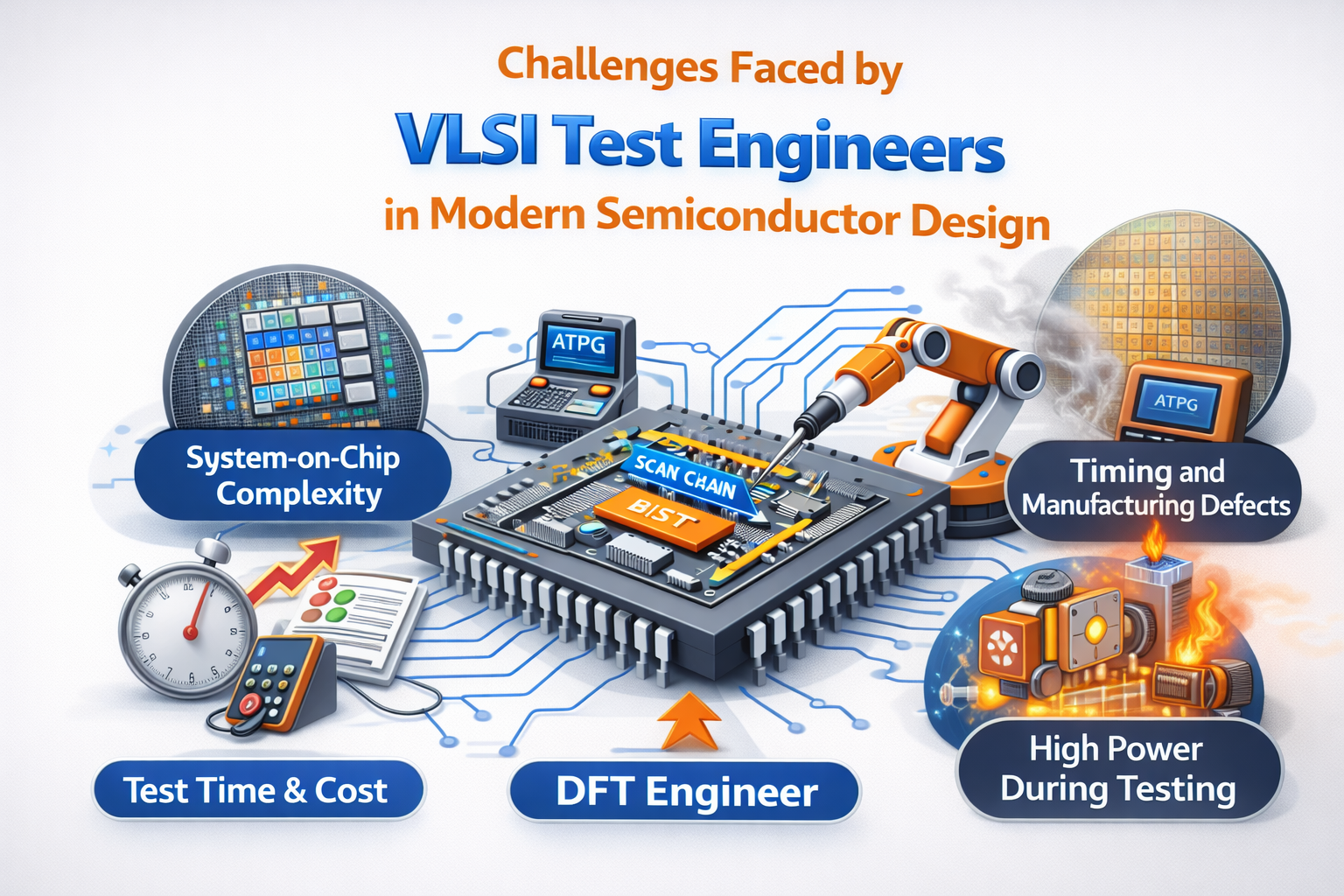
One of the major challenges faced by VLSI test engineers in modern semiconductor design is the rapidly increasing complexity of integrated circuits. Modern chips used in applications such as artificial intelligence, high-performance computing, and automotive electronics can contain billions of transistors and multiple functional blocks within a single System-on-Chip (SoC). Testing such complex designs requires advanced techniques like scan-based testing, Built-In Self-Test (BIST), and Automatic Test Pattern Generation (ATPG) to achieve high fault coverage. As technology nodes continue to shrink, detecting subtle manufacturing defects, timing faults, and power-related issues becomes more difficult, making the testing process more sophisticated and time-consuming.
Another significant challenge is managing test cost, test time, and power consumption during testing. Large chips require a massive number of test patterns to detect potential faults, which can increase production testing time and manufacturing costs. Additionally, applying test patterns can lead to higher switching activity in the circuit, resulting in excessive power consumption during testing, which may damage the chip or produce inaccurate results. To address these issues, VLSI test engineers must develop efficient test architectures, optimize scan chain configurations, and implement power-aware testing techniques. Balancing test coverage, cost, and performance is a key challenge that engineers must solve to ensure reliable and cost-effective semiconductor production.
Conclusion
The role of a VLSI DFT and Test Engineer has become increasingly important in the modern semiconductor industry as chip complexity continues to grow. From implementing scan chains and ATPG techniques to analyzing fault coverage and ensuring manufacturability, DFT engineers play a crucial role in delivering reliable and high-quality integrated circuits. Their work ensures that chips used in technologies such as artificial intelligence, automotive electronics, consumer devices, and communication systems function correctly and meet industry standards. With strong knowledge of digital design, testing methodologies, and EDA tools, professionals in this field contribute significantly to improving chip reliability and reducing production costs.
As the global demand for semiconductors continues to rise, the need for skilled VLSI DFT and Test Engineers is expected to grow steadily. Emerging technologies such as advanced process nodes, System-on-Chip (SoC) designs, and AI-driven hardware are creating new challenges and opportunities in chip testing. For aspiring engineers, building a strong foundation in VLSI concepts, learning modern DFT techniques, and gaining hands-on experience with industry tools can open the door to a rewarding and future-proof career. With continuous learning and practical expertise, VLSI DFT engineers can play a key role in shaping the future of semiconductor innovation.