
Mastering Hardware Debugging: A Professional Guide to JTAG, SWD, and UART for AI-on-Edge Systems
Navigate through this article using the table of contents below
Table of Contents
No headings found in this article.
Mastering hardware debugging is a critical skill in today’s rapidly evolving world of AI-on-Edge systems, where real-time processing, low power consumption, and high reliability are non-negotiable. As embedded systems become more complex, engineers must rely on robust debugging interfaces like JTAG, SWD, and UART to identify, analyze, and resolve hardware and firmware issues efficiently. Whether you're working on microcontrollers, SoCs, or edge AI devices, understanding these debugging protocols is essential for reducing development time, improving system performance, and ensuring product reliability in production environments.
This comprehensive guide to hardware debugging explores the practical applications and differences between JTAG (Joint Test Action Group), SWD (Serial Wire Debug), and UART (Universal Asynchronous Receiver/Transmitter), providing deep insights into how each interface is used in modern embedded and AI-driven systems. From low-level register access and real-time debugging to serial communication and logging, this article is designed to help engineers, students, and professionals build a strong foundation in debugging techniques. By mastering these tools, you can significantly enhance your ability to troubleshoot complex hardware issues and accelerate innovation in AI-on-Edge development. To build a strong foundation in hardware debugging and embedded development, you can explore a structured Embedded Systems with ARM Cortex course .
Introduction to Hardware Debugging in AI-on-Edge Systems

Hardware debugging is a foundational aspect of developing reliable AI-on-Edge systems, where processing is performed locally on embedded devices rather than in the cloud. These systems, often powered by microcontrollers, SoCs, and specialized AI accelerators, demand high performance, low latency, and energy efficiency. However, their complexity introduces challenges such as hardware-software integration issues, signal timing errors, and peripheral misconfigurations. Hardware debugging enables engineers to diagnose these issues at a low level using interfaces like JTAG, SWD, and UART, ensuring that the system operates as intended. Effective debugging not only improves system stability but also accelerates development cycles in edge AI applications such as smart cameras, IoT devices, and autonomous systems.
In modern embedded design workflows, hardware debugging plays a crucial role throughout the product lifecycle—from initial prototyping to post-silicon validation and field deployment. Tools such as debug probes, logic analyzers, and serial communication interfaces allow developers to monitor internal registers, trace execution flow, and capture real-time data. For AI-on-Edge systems, where performance optimization and real-time decision-making are critical, mastering debugging techniques becomes even more important. By understanding how to leverage debugging protocols and tools effectively, engineers can quickly identify bottlenecks, resolve faults, and build robust, scalable edge AI solutions that meet industry demands.
What is JTAG? Understanding Boundary Scan and Debugging Capabilities
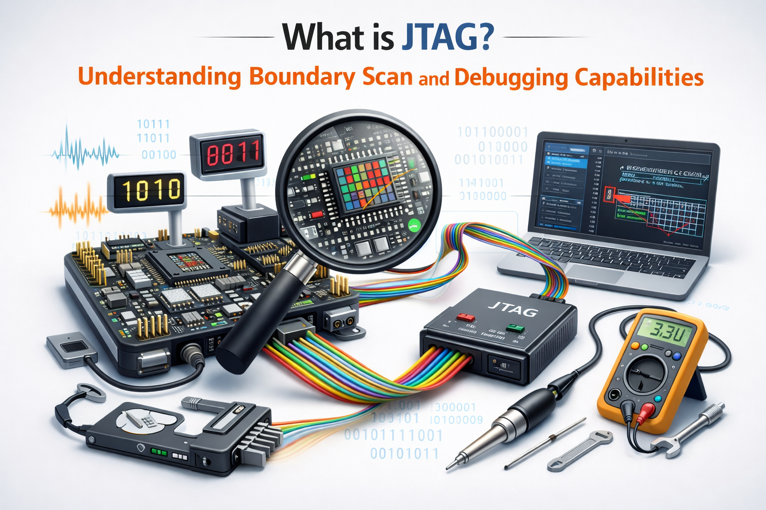
JTAG (Joint Test Action Group) is a widely used hardware interface standard, formally defined as IEEE 1149.1, designed for testing, debugging, and verifying digital circuits on printed circuit boards (PCBs). Originally developed for boundary scan testing, JTAG enables engineers to access internal registers and signals of integrated circuits without requiring physical probing of each pin. This makes it especially valuable in modern high-density designs such as microcontrollers, FPGAs, and SoCs used in AI-on-Edge systems. By connecting a JTAG debugger or probe, developers can interact directly with the processor, halt execution, inspect memory, and control program flow at a very granular level.
One of the key features of JTAG is boundary scan, a technique that allows testing of interconnections between ICs on a PCB. Each JTAG-enabled device contains a series of boundary scan cells connected in a chain, forming a scan path that can shift test data through the device’s pins. This capability enables detection of faults such as open circuits, short circuits, and incorrect connections without the need for complex test fixtures. Boundary scan is particularly important in advanced semiconductor manufacturing and PCB assembly, where traditional testing methods are limited due to miniaturization and multilayer board designs.
Beyond manufacturing test, JTAG is extensively used for in-system debugging and firmware development. Engineers can use JTAG to set breakpoints, step through code, monitor CPU registers, and analyze system behavior in real time. It also supports advanced features like flash programming and trace debugging, which are essential for optimizing performance in embedded and AI-driven applications. In AI-on-Edge systems, where reliability and efficiency are critical, JTAG provides a powerful and flexible interface to diagnose complex hardware and software issues, making it an indispensable tool in the embedded development workflow. These debugging techniques are also widely used in modern chip architectures, which you can learn in depth through a System-on-Chip (SoC) Design training program.
SWD vs JTAG: Key Differences and When to Use Each Interface
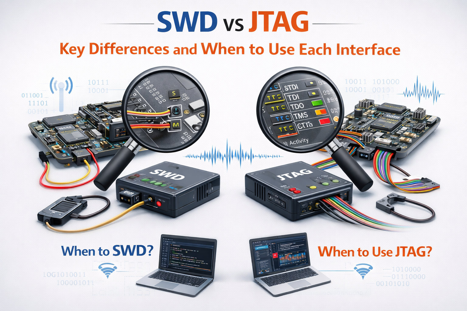
SWD (Serial Wire Debug) and JTAG are two widely used hardware debugging interfaces in embedded systems, but they differ significantly in architecture, pin usage, and application scope. JTAG is a standardized interface (IEEE 1149.1) that uses multiple pins (typically TCK, TMS, TDI, TDO) and supports advanced features such as boundary scan testing, multi-device chaining, and deep system-level debugging. In contrast, SWD is a simplified two-wire protocol (SWDIO and SWCLK) developed by ARM, designed specifically for debugging ARM-based microcontrollers. SWD offers similar core debugging capabilities—such as breakpoints, memory access, and register inspection—while reducing pin count and board complexity, making it ideal for compact and cost-sensitive AI-on-Edge devices.
When deciding between SWD and JTAG, the choice depends on system requirements and design constraints. SWD is generally preferred for modern embedded systems using ARM Cortex-M processors due to its efficiency, lower power consumption, and minimal pin usage, which is crucial in space-constrained designs like IoT and edge AI devices. On the other hand, JTAG is better suited for complex systems involving multiple devices, FPGA debugging, or when boundary scan testing is required during manufacturing and validation. While SWD excels in streamlined debugging for single-chip systems, JTAG remains indispensable in scenarios that demand extensive testing, chaining, and advanced diagnostic capabilities across larger and more complex hardware platforms.
Understanding UART Communication for Debugging and Logging in Embedded Systems

UART (Universal Asynchronous Receiver/Transmitter) is one of the most fundamental and widely used communication protocols in embedded systems, particularly for debugging and logging purposes. Unlike synchronous interfaces, UART operates without a shared clock, relying instead on predefined baud rates to transmit data between devices. It uses two primary lines—TX (transmit) and RX (receive)—making it simple to implement and highly effective for real-time communication. In embedded development, UART is commonly used to output debug messages, monitor system behavior, and interact with firmware during development and testing phases, especially in AI-on-Edge systems where visibility into internal processes is critical.
For debugging, UART serves as a lightweight and non-intrusive method to trace program execution and capture runtime information. Developers often use serial terminals to view logs such as variable values, error messages, and system states, which helps in identifying bugs and performance bottlenecks. Unlike JTAG or SWD, which provide deep access to internal registers and execution control, UART focuses on communication-based debugging, making it ideal for quick diagnostics and field-level troubleshooting. It is particularly useful in scenarios where hardware debugging interfaces are limited or unavailable, allowing engineers to still gain insights into system functionality.
In addition to debugging, UART plays a crucial role in system logging and firmware communication in embedded and AI-driven applications. It is frequently used for bootloader communication, firmware updates, and interfacing with external modules such as GPS, Bluetooth, and sensors. Its simplicity, low cost, and widespread support across microcontrollers make UART an essential tool in the embedded ecosystem. By effectively leveraging UART for logging and communication, engineers can enhance system transparency, improve debugging efficiency, and ensure reliable operation of complex embedded systems in real-world environments.
Role of Hardware Debugging in Embedded Systems and Edge AI Development
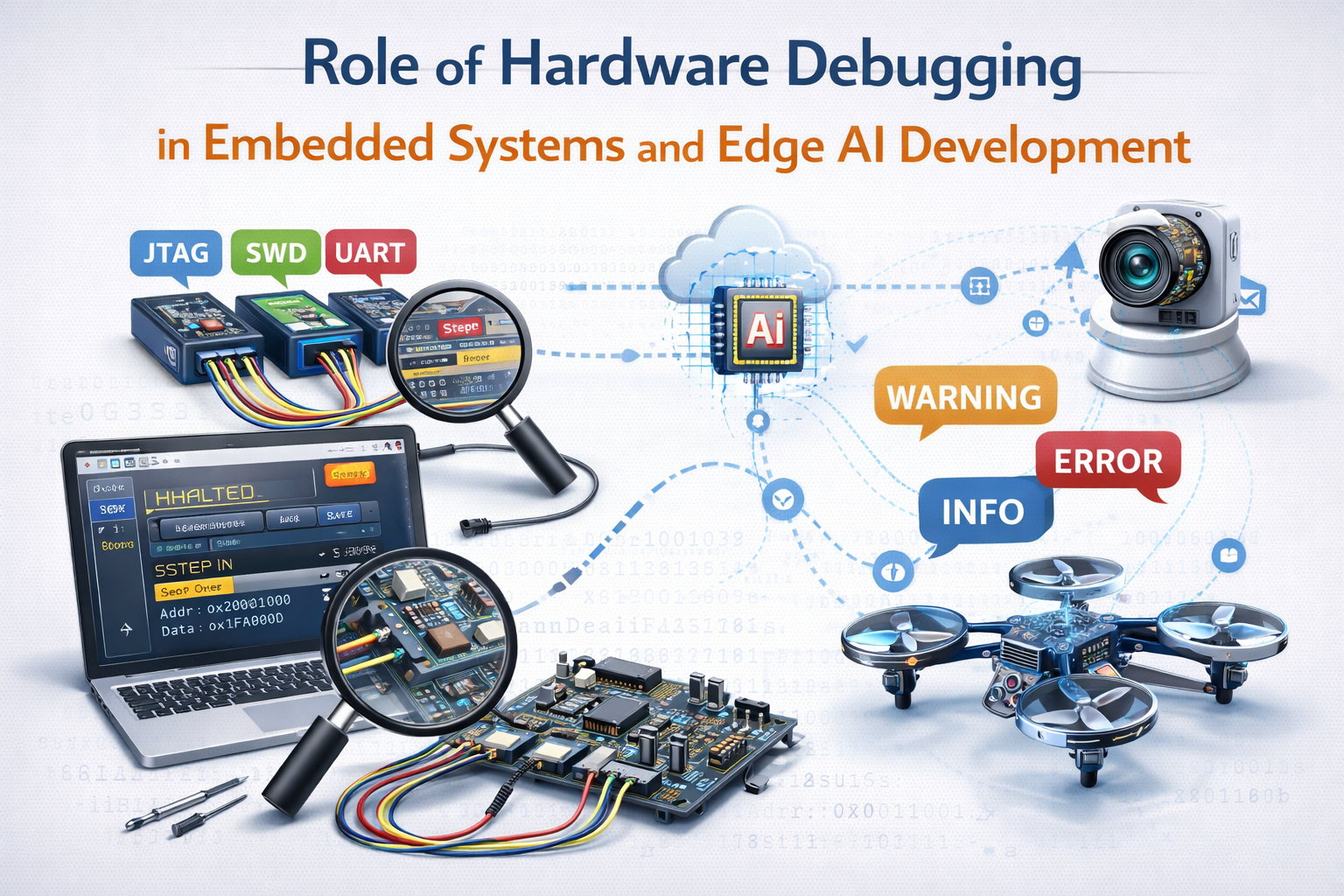
Hardware debugging plays a pivotal role in embedded systems and Edge AI development by enabling engineers to identify, isolate, and resolve issues at both the hardware and firmware levels. As embedded devices become more complex—with integrated processors, memory, sensors, and AI accelerators—ensuring correct interaction between components is critical. Debugging interfaces such as JTAG, SWD, and UART allow developers to monitor internal signals, inspect registers, and trace program execution in real time. This level of visibility is essential for diagnosing issues like timing violations, peripheral misconfigurations, and hardware-software integration bugs, ultimately improving system reliability and reducing development time. Institutes like JastTech help engineers build strong practical debugging skills required in real-world projects.
In Edge AI applications, where systems must process data locally with minimal latency and high efficiency, hardware debugging becomes even more crucial. Engineers need to optimize performance, power consumption, and memory usage while maintaining accuracy in AI inference tasks. Debugging tools help uncover bottlenecks, validate data flow between AI models and hardware, and ensure stable operation under real-world conditions. From prototyping to production and field deployment, effective hardware debugging ensures that embedded and Edge AI systems perform reliably, meet industry standards, and deliver consistent results in applications such as smart devices, autonomous systems, and industrial IoT.
Step-by-Step Hardware Debugging Process Using JTAG, SWD, and UART
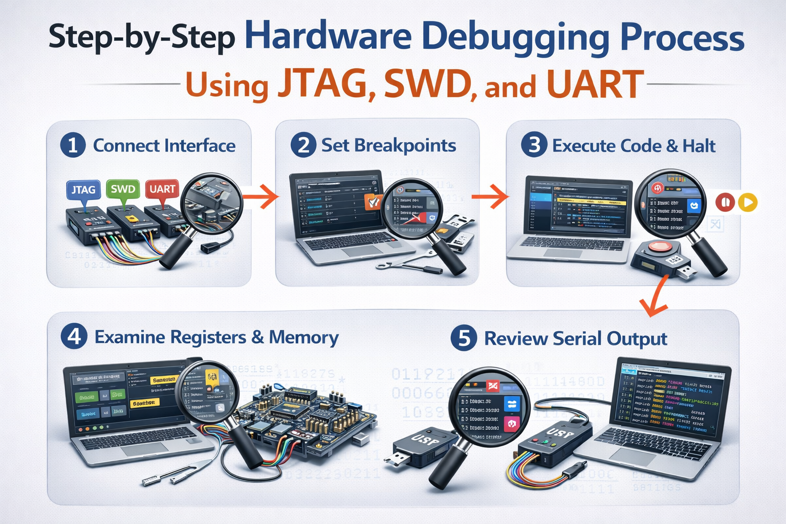
A step-by-step hardware debugging process using JTAG, SWD, and UART begins with establishing basic board bring-up and connectivity checks. Engineers first verify power rails, clock signals, reset behavior, and physical connections on the PCB to ensure the hardware is ready for debugging. Once the board powers up correctly, a debug probe is connected through JTAG or SWD to confirm that the processor or microcontroller is detectable. At this stage, developers typically check whether the device can be identified, memory can be accessed, and firmware can be loaded successfully. This initial setup is critical because many hardware issues, such as improper soldering, unstable power, or incorrect pin mapping, can prevent deeper debugging from working at all.
The next step involves using JTAG or SWD for low-level debugging of the target system. Through these interfaces, engineers can halt the processor, set breakpoints, inspect CPU registers, read and write memory, and step through firmware execution line by line. This helps identify where the system is failing, whether due to boot errors, peripheral initialization problems, or software logic faults. JTAG is especially useful in more complex systems requiring boundary scan and multi-device testing, while SWD is commonly preferred for ARM-based embedded systems because of its simpler two-wire design. During this phase, developers often compare expected versus actual register values and trace the execution path to isolate the exact source of the malfunction.
UART is then used alongside JTAG or SWD to provide real-time logging and runtime visibility into system behavior. By printing debug messages, error codes, sensor readings, or state transitions to a serial terminal, engineers can observe how the firmware behaves during normal operation without constantly stopping execution. This is especially useful for tracking intermittent bugs, communication failures, and performance bottlenecks in embedded and AI-on-Edge systems. In practice, the most effective debugging workflow combines all three interfaces: JTAG or SWD for deep control and inspection, and UART for continuous logging and monitoring. By following this structured debugging process, engineers can diagnose problems faster, reduce development risk, and build more reliable embedded hardware products.
Common Hardware Debugging Challenges in AI-on-Edge Devices and How to Solve Them
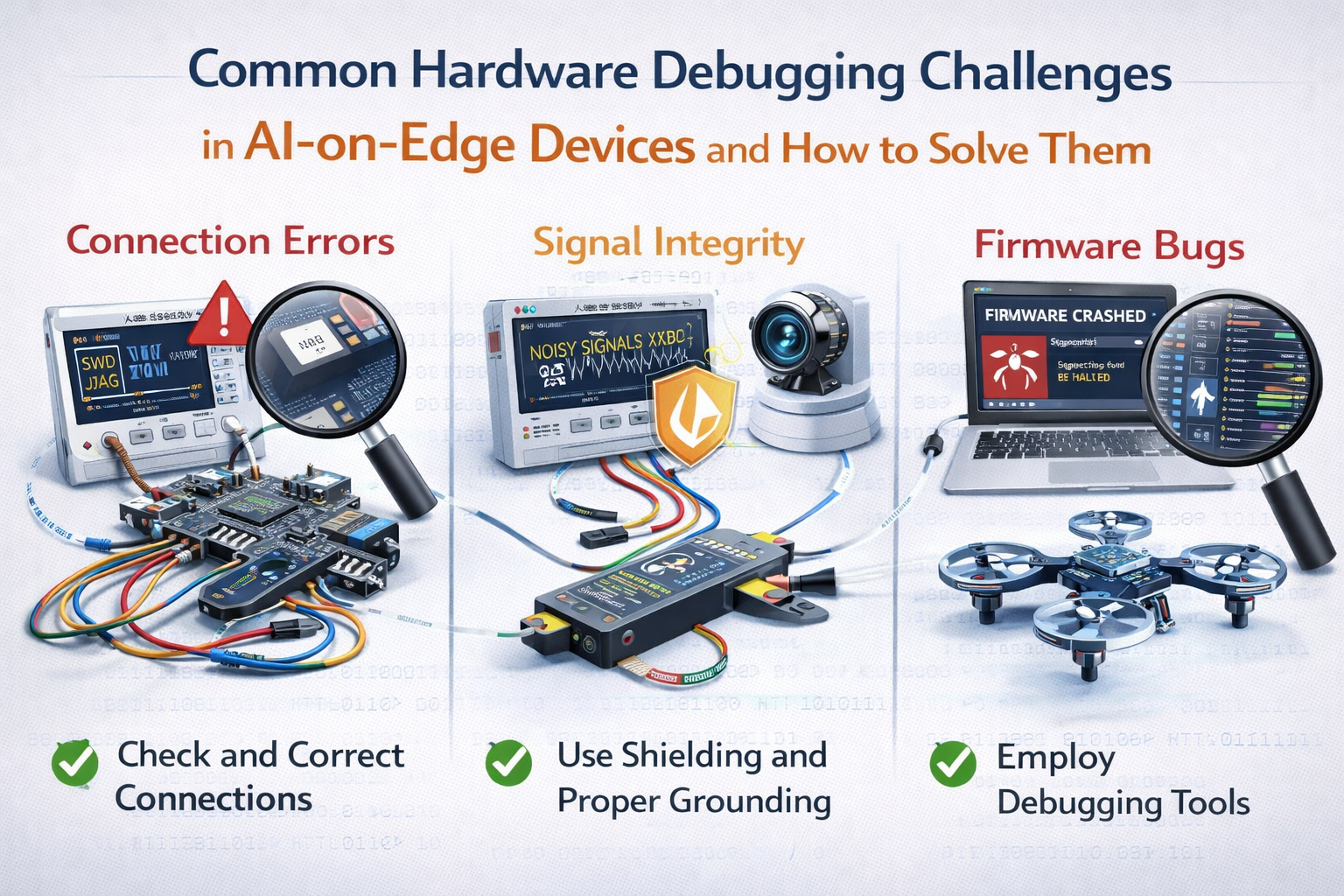
AI-on-Edge devices introduce several hardware debugging challenges due to their high integration, real-time processing requirements, and tight power constraints. One of the most common issues is hardware-software integration failure, where mismatches between firmware initialization and hardware configuration lead to system crashes or unpredictable behavior. Signal integrity problems, such as noise, crosstalk, and timing violations, are also prevalent in high-speed interfaces and densely packed PCBs. Additionally, limited visibility into internal system states—especially in compact edge devices—makes it difficult to trace faults using traditional methods. Power-related issues, including unstable voltage rails and improper power sequencing, can further complicate debugging by causing intermittent failures that are hard to reproduce.
To address these challenges, engineers adopt a systematic and multi-layered debugging approach. Using JTAG or SWD enables deep access to processor registers and memory, helping identify initialization errors and execution faults, while UART provides continuous logging for tracking runtime behavior. Signal integrity issues can be mitigated using tools like oscilloscopes and logic analyzers to validate timing and waveform quality. For power-related problems, proper power rail monitoring and decoupling techniques are essential. Additionally, implementing structured debug logs, modular firmware design, and test points on PCBs significantly improves observability and fault isolation. By combining the right tools with disciplined debugging methodologies, developers can effectively overcome these challenges and ensure reliable performance of AI-on-Edge systems in real-world applications.
Tools and Equipment for Hardware Debugging: Debug Probes, Logic Analyzers, and IDEs

Hardware debugging in embedded systems and AI-on-Edge development relies heavily on specialized tools and equipment that provide deep visibility and control over system behavior. Debug probes are one of the most essential tools, enabling communication between the development environment and the target hardware through interfaces like JTAG and SWD. These probes allow engineers to halt execution, set breakpoints, inspect memory and registers, and program firmware directly onto the device. Popular debug probes are designed to support a wide range of microcontrollers and processors, making them indispensable for low-level debugging, especially during early development and board bring-up stages.
Logic analyzers are another critical tool used to capture and analyze digital signals across multiple channels simultaneously. They are particularly useful for debugging communication protocols such as UART, SPI, and I2C, where timing and data integrity are crucial. By visualizing signal transitions and decoding protocol data, engineers can identify issues like incorrect timing, data corruption, or synchronization errors. In AI-on-Edge systems, where multiple peripherals and high-speed interfaces interact, logic analyzers help validate communication between components and ensure that the system operates as expected under real-time conditions.
Integrated Development Environments (IDEs) complement hardware tools by providing a software interface for coding, debugging, and system analysis. IDEs such as Keil, IAR Embedded Workbench, and VS Code (with embedded extensions) integrate seamlessly with debug probes to offer features like real-time variable monitoring, call stack analysis, and performance profiling. These environments streamline the debugging workflow by combining code editing, compilation, and debugging into a single platform. When used together, debug probes, logic analyzers, and IDEs form a powerful ecosystem that enables engineers to efficiently diagnose issues, optimize performance, and develop robust embedded and AI-driven hardware systems.
Best Practices for Efficient Hardware Debugging in Modern Embedded Systems
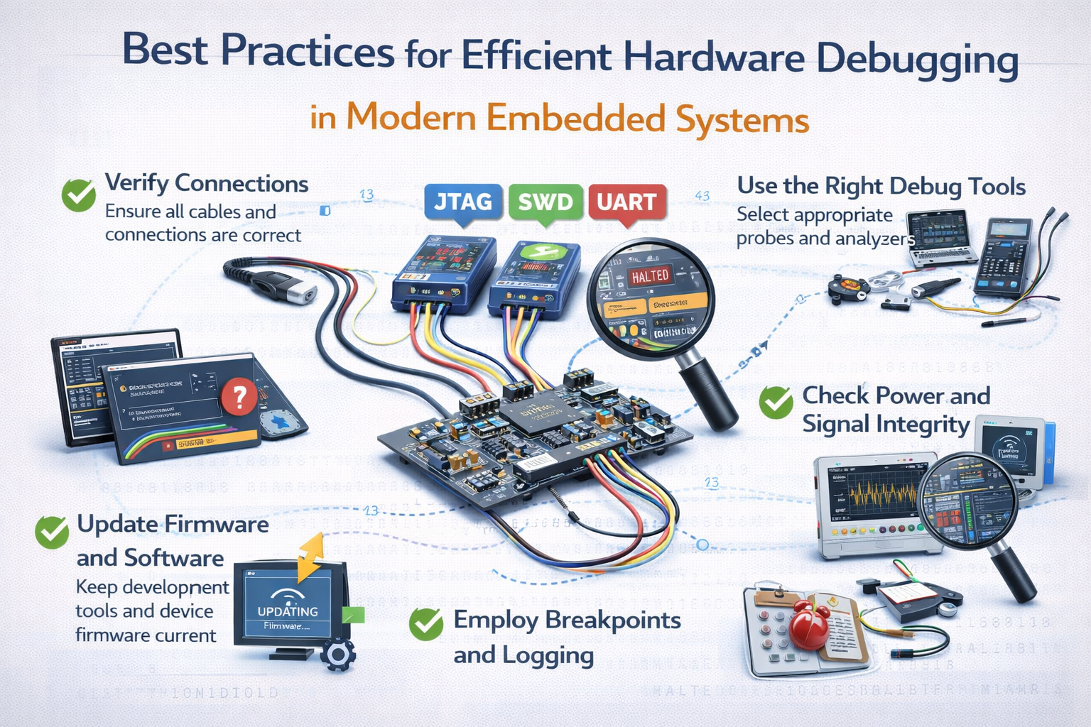
Efficient hardware debugging in modern embedded systems requires a structured and methodical approach that begins early in the design phase. One of the key best practices is designing for debug by incorporating test points, accessible debug interfaces (JTAG/SWD/UART), and proper labeling on the PCB. Engineers should follow a systematic debugging strategy—starting with power, clock, and reset verification before moving to peripheral and firmware-level checks. Maintaining clean and modular code, along with meaningful debug logs via UART, significantly improves visibility into system behavior. Additionally, using version control and documenting known issues helps teams track changes and avoid repeating the same debugging cycles.
Another important practice is leveraging the right combination of tools and techniques to isolate issues quickly and accurately. Debug probes should be used for low-level inspection and control, while logic analyzers and oscilloscopes help analyze signal integrity and communication timing. Engineers should also validate assumptions at each stage, compare expected versus actual behavior, and test subsystems independently to reduce complexity. In AI-on-Edge systems, where performance and reliability are critical, optimizing debugging workflows and automating repetitive tests can save significant development time. By following disciplined debugging practices and continuously refining their approach, engineers can build more stable, efficient, and scalable embedded systems.
Future Scope of Hardware Debugging in AI, IoT, and Edge Computing Systems

The future scope of hardware debugging in AI, IoT, and edge computing systems is expanding rapidly as devices become more intelligent, interconnected, and complex. With the rise of AI-on-Edge applications such as smart surveillance, autonomous systems, wearable devices, and industrial IoT, the demand for advanced debugging techniques is increasing. Modern systems integrate heterogeneous components including CPUs, GPUs, NPUs, and specialized accelerators, making traditional debugging approaches insufficient. As a result, next-generation debugging solutions are evolving to include real-time trace analysis, AI-assisted debugging, and enhanced visibility into system-level interactions. These advancements will enable engineers to diagnose issues faster, optimize performance, and ensure reliability in highly dynamic and distributed environments.
In addition, the growing emphasis on low-power design, security, and remote deployment is shaping the future of hardware debugging methodologies. Techniques such as remote debugging, over-the-air (OTA) diagnostics, and cloud-connected debug frameworks are becoming essential for managing large-scale IoT and edge deployments. Debugging tools are also being integrated with machine learning algorithms to predict failures, detect anomalies, and automate root-cause analysis. As semiconductor technologies continue to advance toward smaller nodes and more complex architectures, hardware debugging will remain a critical skill for engineers. Those who master modern debugging tools and methodologies will play a key role in driving innovation and ensuring the robustness of next-generation AI and edge computing systems.
Conclusion
Hardware debugging is an indispensable skill in modern embedded systems and AI-on-Edge development, enabling engineers to ensure system reliability, performance, and scalability. From understanding core debugging interfaces like JTAG, SWD, and UART to applying structured debugging methodologies, each aspect plays a crucial role in identifying and resolving complex hardware and firmware issues. As systems become more integrated and performance-driven, the ability to effectively debug at both low-level and system-level becomes a key differentiator for engineers working in the semiconductor and embedded domains.
As the industry continues to evolve with advancements in AI, IoT, and edge computing, hardware debugging will remain a critical component of the development lifecycle. Emerging tools, automation techniques, and AI-assisted debugging approaches are set to transform how engineers diagnose and optimize systems in the future. By mastering the concepts, tools, and best practices discussed in this guide, professionals and students can build a strong foundation in hardware debugging and stay ahead in the rapidly growing field of embedded and AI-driven technologies.