

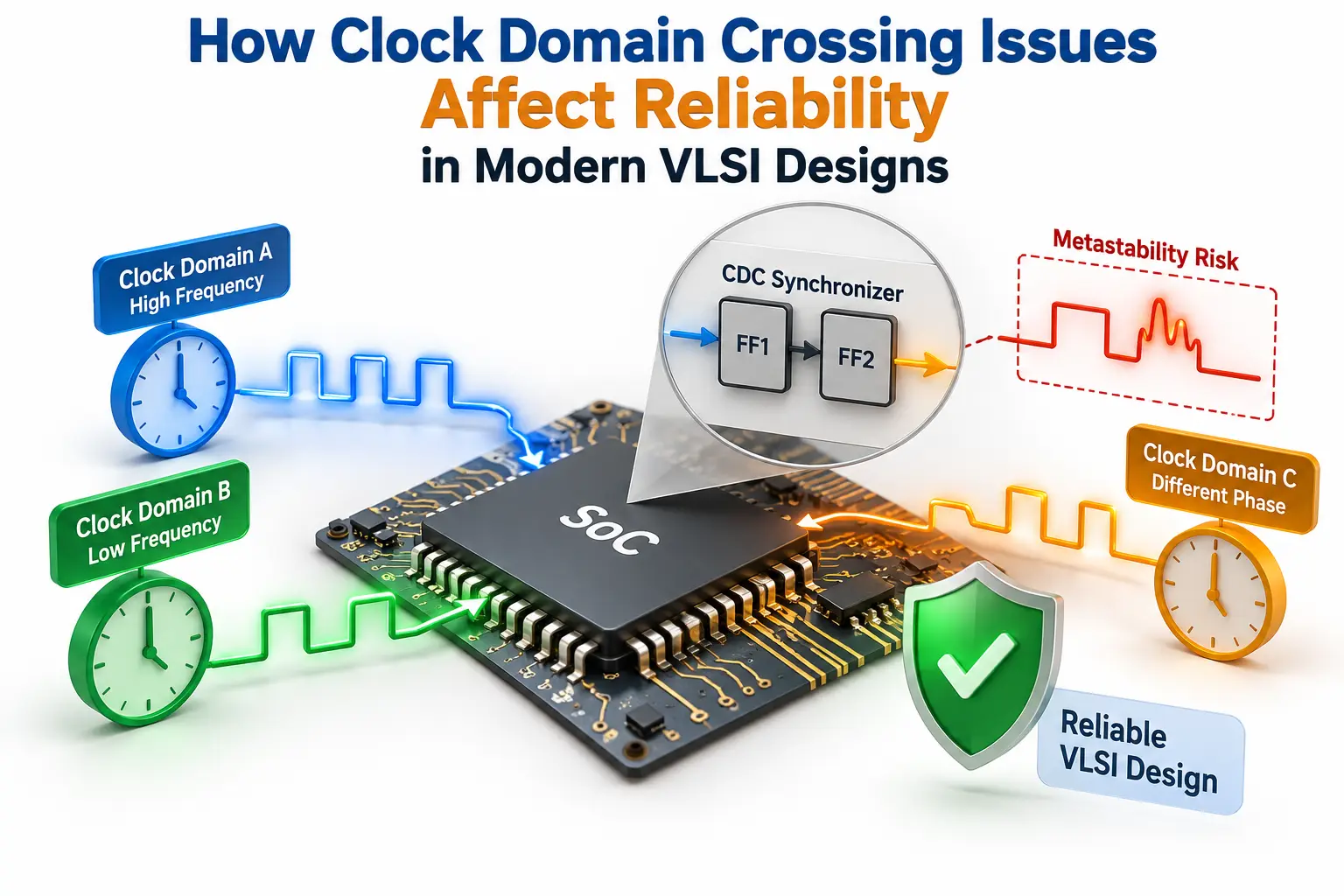
How Clock Domain Crossing Issues Affect Reliability in Modern VLSI Designs
Navigate through this article using the table of contents below
Table of Contents
No headings found in this article.
A chip can pass functional simulation, meet timing requirements, and still fail because of something happening between two clock domains. This hidden challenge is called Clock Domain Crossing (CDC), and it plays a critical role in modern semiconductor reliability.
As VLSI architectures become increasingly complex, multiple clock domains are unavoidable. Understanding how signals move between these domains is essential for preventing metastability, data corruption, and unpredictable hardware failures.
Understanding Clock Domain Crossing in Modern VLSI Designs
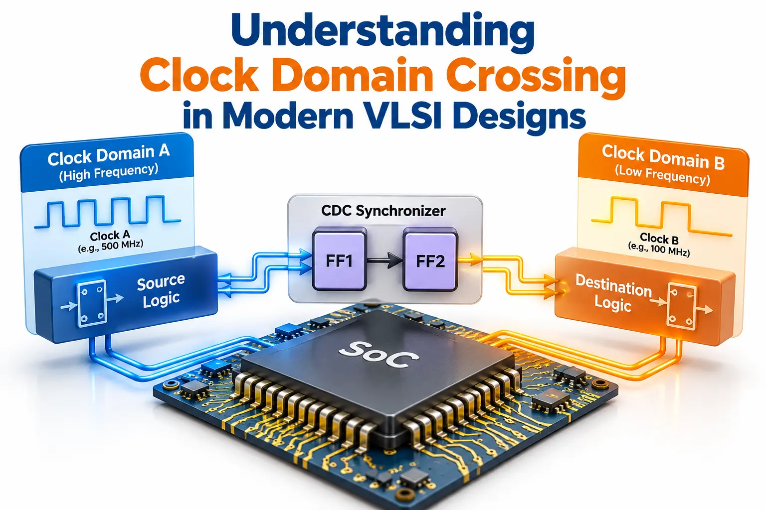
Clock Domain Crossing occurs when a signal transfers from one clock domain to another. Each domain operates using its own clock signal, which may have a different frequency, phase, or timing relationship.
Modern System-on-Chip (SoC) architectures commonly contain several clock domains because different functional blocks have different performance and power requirements.
For example, a processor may operate at a high frequency while its peripheral interface operates at a much lower frequency. When these blocks exchange information, the receiving domain must correctly capture signals generated by the transmitting domain.
The main challenge is that the destination clock may not be synchronized with the source clock.
Common situations requiring CDC handling include:
Processor-to-peripheral communication.
Communication between CPU and memory controllers.
High-speed interfaces connecting different subsystems.
Data transfers between independently clocked IP blocks.
Power-managed blocks operating at different frequencies.
Without appropriate synchronization techniques, signals may be captured incorrectly, creating functional failures that are difficult to reproduce during simulation.
How Metastability Becomes a Major Reliability Challenge
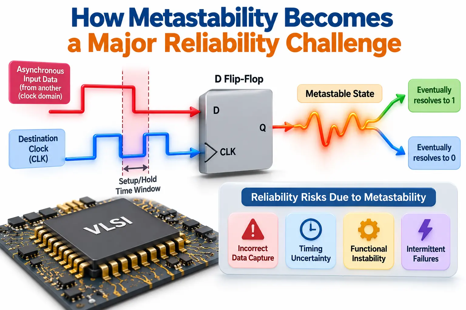
Metastability is one of the most important problems associated with asynchronous clock crossings.
A flip-flop requires its input data to remain stable during specific setup and hold time intervals around the active clock edge. When an asynchronous signal changes close to the destination clock edge, these requirements may be violated.
The flip-flop can temporarily enter a metastable state, where its output does not immediately resolve to a valid logic zero or one.
Although the output generally settles to a stable value, the resolution time is unpredictable.
This creates several reliability risks:
Incorrect data capture: Downstream logic may receive an unexpected value.
Timing uncertainty: The metastable output may take longer than expected to settle.
Functional instability: Different parts of the receiving logic may observe inconsistent information.
Intermittent failures: A design may work during normal testing but fail under specific operating conditions.
A two-stage synchronizer is commonly used for single-bit control signals. The first flip-flop captures the asynchronous input, while the second provides additional time for metastability to resolve.
However, synchronizers do not eliminate metastability. They reduce the probability of metastability propagating into downstream logic.
Designers evaluate this reliability using Mean Time Between Failures (MTBF). Higher MTBF generally indicates a lower probability of synchronization failure.
Data Loss and Data Corruption in Multi-Bit Clock Crossings
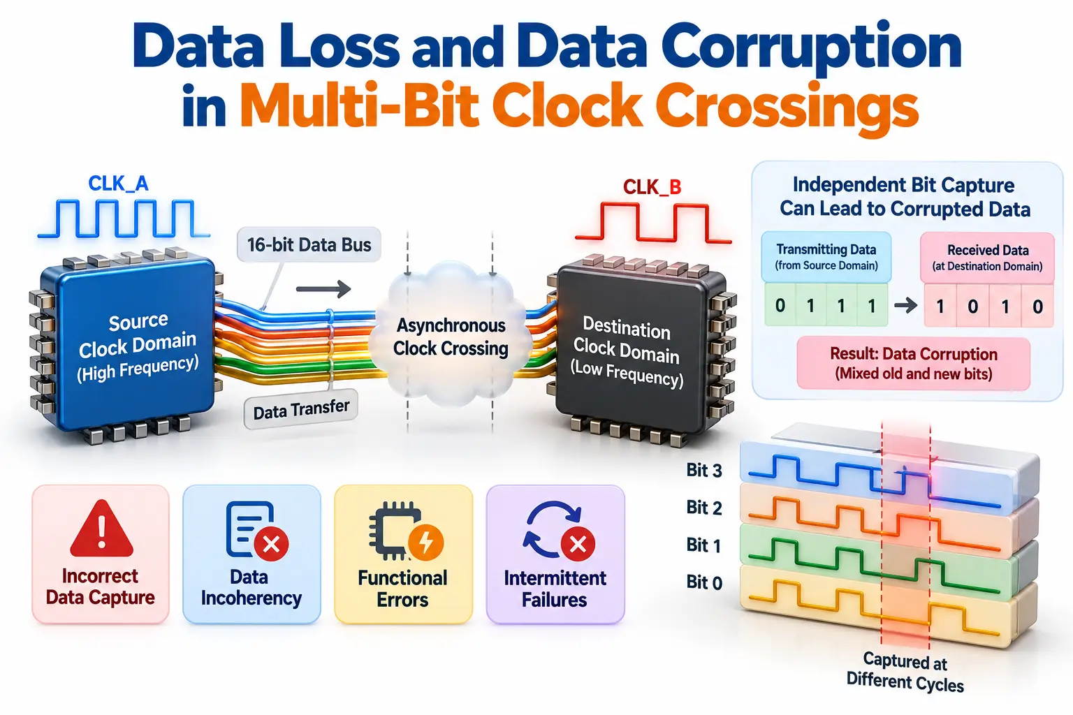
Synchronizing a single-bit signal is relatively straightforward. However, transferring multiple bits between asynchronous clock domains introduces additional challenges.
Consider a 16-bit data bus transferring information from one clock domain to another. If every bit is synchronized independently, different bits may settle during different destination clock cycles.
The receiving circuit could therefore capture a combination of old and new data.
This problem is known as data incoherency.
For example, suppose a source domain transfers the binary value 0111 to 1000. If individual bits are captured at different times, the destination domain may temporarily observe an unintended intermediate value.
Such errors can affect:
Address information transferred between functional blocks.
Configuration registers.
Processor-to-memory communication.
Control and status information.
High-speed data interfaces.
Several techniques are used to prevent these problems.
Common CDC solutions include:
Gray Coding: Only one bit changes between consecutive values, reducing the risk of inconsistent pointer sampling.
Handshake Synchronization: Request and acknowledgment signals coordinate data transfers between clock domains.
Asynchronous FIFO: Independent write and read clock domains allow reliable data buffering and transfer.
Stable Data Transfer: The source holds the data constant while the destination captures it using an appropriate control protocol.
The correct method depends on data width, transfer frequency, latency requirements, and the communication protocol.
CDC Synchronization Techniques That Improve Chip Reliability
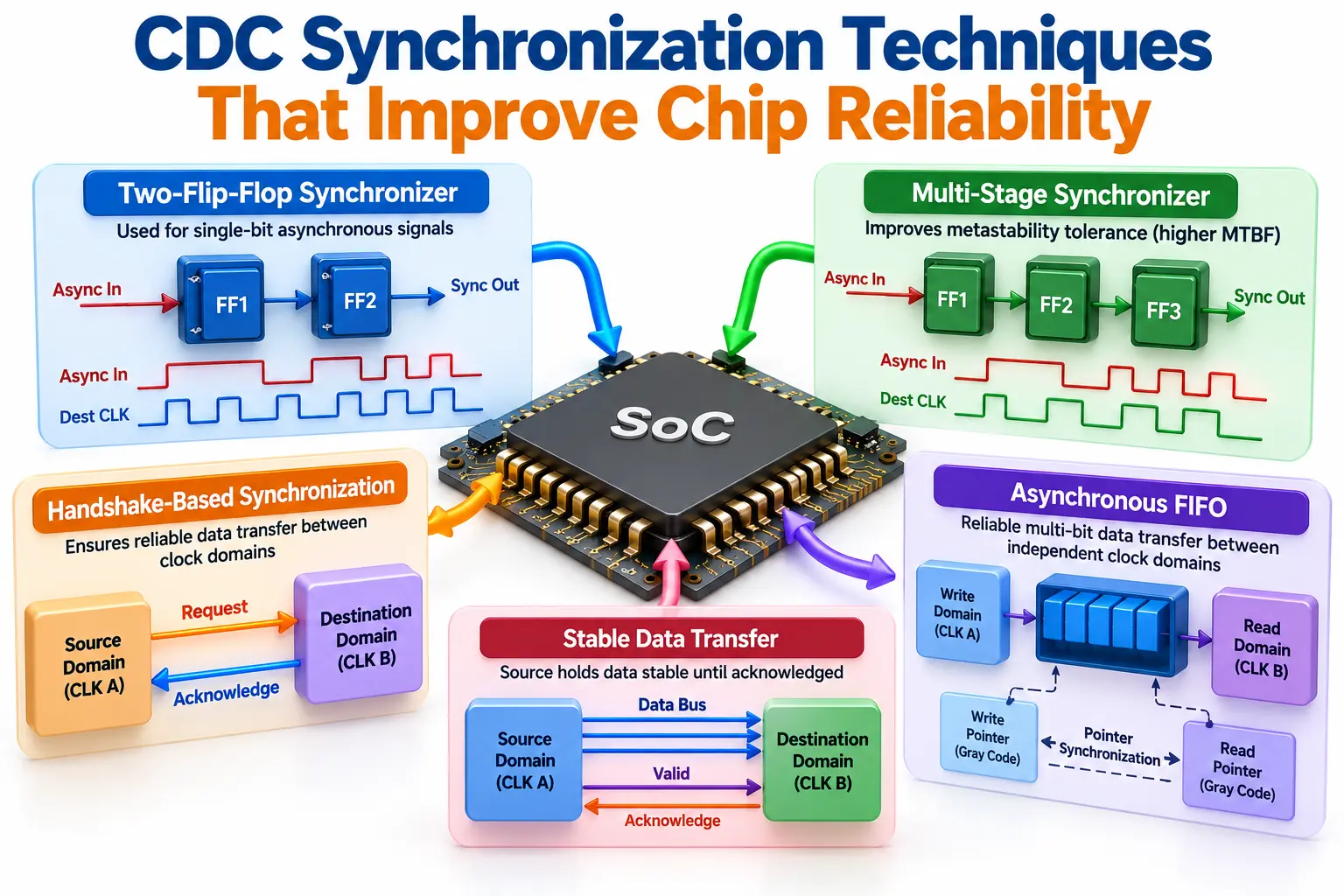
Choosing the correct synchronization architecture is essential for building reliable VLSI systems. A synchronization method suitable for a single-bit interrupt signal may not work for a wide data bus.
Engineers must understand the behavior of the signals before selecting an implementation.
Important synchronization techniques include:
Two-Flip-Flop Synchronizer
This is commonly used for single-bit asynchronous control signals.
The receiving clock domain captures the signal through two consecutive flip-flops, providing additional metastability resolution time.
Multi-Stage Synchronizer
Additional flip-flop stages can improve metastability tolerance when the reliability requirements justify the extra latency and area.
Handshake-Based Synchronization
A request-and-acknowledgment mechanism ensures that the source and destination domains coordinate the transfer. It is useful when transferring data without losing information.
Asynchronous FIFO
Asynchronous FIFOs are widely used when transferring continuous or multiple-bit data between unrelated clock domains.
They typically use separate read and write pointers, Gray-coded pointer synchronization, and appropriate full and empty detection logic.
When implementing these structures, engineers should consider:
Synchronizer depth and MTBF requirements.
Source and destination clock frequencies.
Reset behavior across clock domains.
Signal stability and reconvergence.
Physical placement of synchronizer flip-flops.
Latency, power, and area constraints.
Selecting a synchronization method based only on the number of flip-flops can create serious reliability problems.
CDC Verification: Finding Problems Before Silicon Fabrication
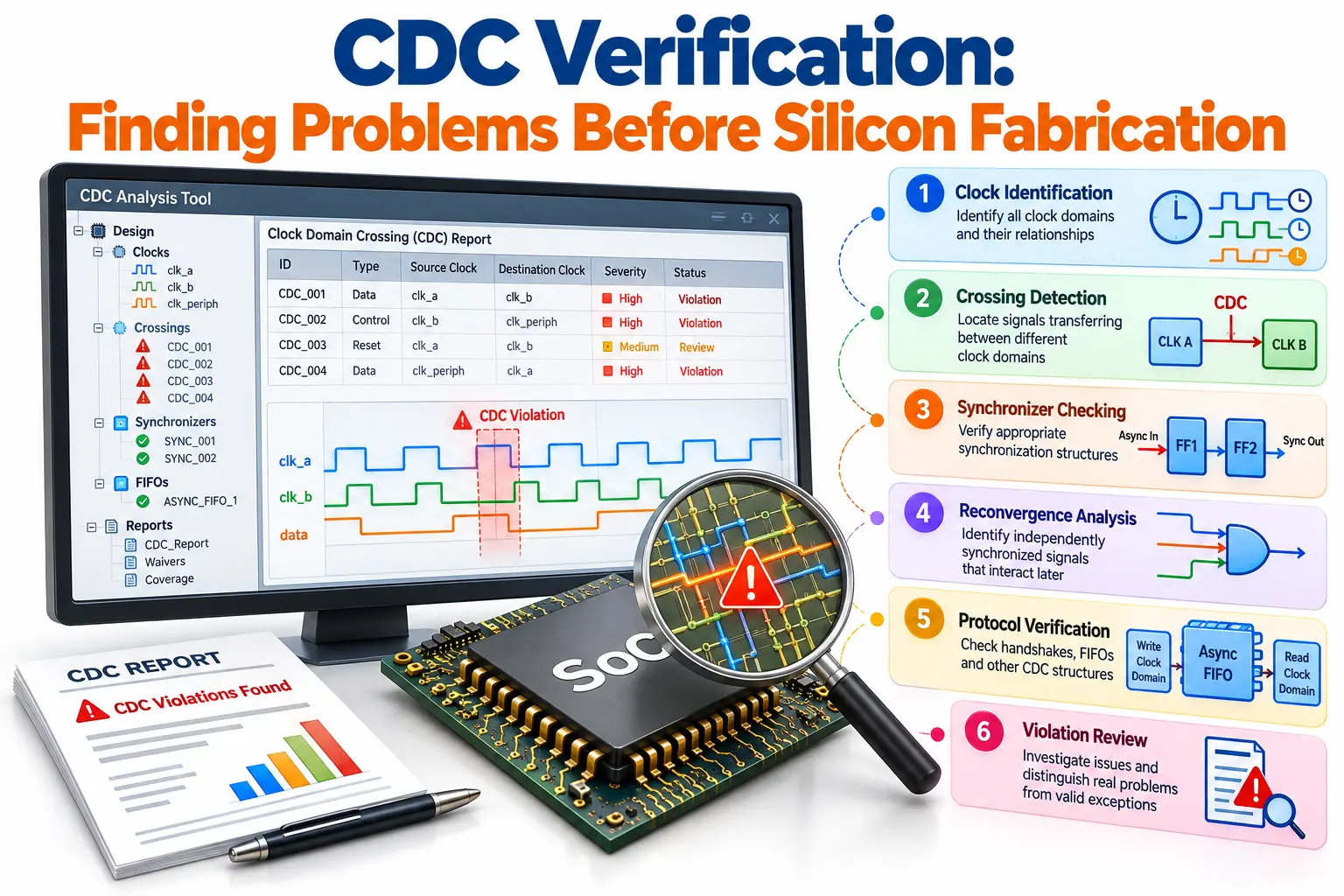
Even a carefully designed RTL architecture can contain CDC violations. Therefore, CDC verification must be included in the design verification process rather than treated as a final-stage activity.
Static CDC analysis tools examine the RTL structure and identify signals crossing between different clock domains.
Unlike conventional simulation, structural CDC analysis does not depend entirely on applying specific input test patterns.
A typical CDC verification workflow includes:
Clock Identification: Identify all clock signals and their relationships.
Crossing Detection: Locate signals transferring between different clock domains.
Synchronizer Checking: Verify whether appropriate synchronization structures exist.
Reconvergence Analysis: Identify independently synchronized signals that interact later in the destination domain.
Protocol Verification: Check whether handshakes, FIFOs, and other synchronization structures operate correctly.
Violation Review: Investigate reported issues and distinguish genuine problems from valid exceptions.
Tools from Cadence, Siemens, and other EDA providers support different aspects of CDC analysis.
Engineers may also use SystemVerilog Assertions (SVA), formal verification, and metastability-aware simulation techniques to verify functional behavior.
It is important to remember that passing structural CDC checks alone does not guarantee complete functional correctness. The communication protocol and reset behavior must also be verified.
For aspiring engineers, learning these concepts through practical RTL exercises is valuable. A structured learning environment such as JastTech can help students understand CDC architecture, RTL coding, and verification workflows. Choosing the Best VLSI Training Institute in Hyderabad can also help learners build practical knowledge of synchronization techniques and industry-relevant verification methodologies.
Best Practices for Building Reliable CDC Architectures
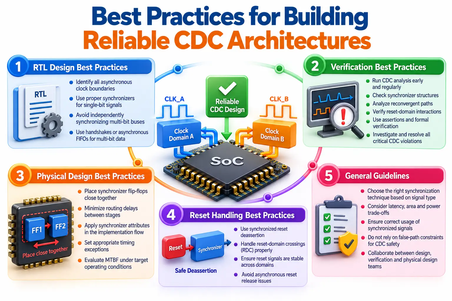
Preventing CDC failures requires collaboration between RTL designers, verification engineers, and physical design teams.
CDC considerations should begin during architecture development because fixing synchronization problems after implementation can increase design complexity and verification effort.
The following practices help improve reliability:
At the RTL Design Stage
Identify every asynchronous clock boundary.
Use appropriate synchronizers for single-bit control signals.
Avoid independently synchronizing ordinary multi-bit data buses.
Implement asynchronous FIFOs or handshake protocols where necessary.
Ensure synchronized signals are used correctly in downstream logic.
At the Verification Stage
Run CDC analysis regularly during RTL development.
Review reconvergent signal paths.
Verify reset-domain interactions.
Check asynchronous FIFO behavior.
Use assertions and formal verification for important protocols.
Investigate every critical CDC violation before signoff.
At the Physical Design Stage
Place synchronizer flip-flops close together to preserve available resolution time.
Minimize routing delays between synchronization stages.
Apply appropriate synchronizer attributes supported by the implementation flow.
Review timing exceptions carefully.
Evaluate MTBF under relevant operating conditions.
One important consideration is that false-path constraints do not make an asynchronous crossing safe. They only influence timing analysis. Proper synchronization architecture and CDC verification are still necessary.
Combining these practices helps reduce synchronization risks and improves the reliability of complex semiconductor devices.
Conclusion
Clock Domain Crossing is much more than a timing consideration in modern VLSI design. It directly influences functional correctness, data integrity, and long-term chip reliability. Metastability, data incoherency, and synchronization failures can create intermittent hardware problems that conventional simulation may not easily identify. Understanding CDC architectures and implementing appropriate synchronization techniques are therefore essential responsibilities of RTL and verification engineers.
As semiconductor designs continue to incorporate multiple clock domains, CDC verification will remain an important part of successful chip development. Engineers who understand synchronizers, asynchronous FIFOs, handshake protocols, MTBF analysis, and CDC verification tools will be better prepared for industry challenges. Through practical learning and structured technical training, JastTech aims to help aspiring VLSI professionals develop the knowledge needed to work confidently with modern semiconductor design methodologies.