



Master chip design at Jasttech, the best VLSI training institute in Noida. Gain hands-on EDA tool labs, expert classroom guidance, and 100% placement support.
Master chip design at Jasttech, the best VLSI training institute in Noida. Gain hands-on EDA tool labs, expert classroom guidance, and 100% placement support.
Level
Advanced
Duration
6 Months
Our Alumni Work At












Looking to launch a core engineering career in semiconductor design? Jasttech stands as an industry-leading vlsi training institute in noida, delivering hands-on classroom education for electronics graduates and working professionals. Strategically located near key technology hubs in Sector 62 and 63, our state-of-the-art facility features fully equipped physical labs running corporate-licensed EDA software.
When you enroll in a specialized vlsi course in noida at Jasttech, you gain practical exposure to RTL modeling, SystemVerilog verification, UVM frameworks, DFT, and Physical Design. Our job-oriented vlsi classes in noida are mentored by senior hardware design engineers with over a decade of active silicon experience, ensuring you bridge the gap between academic theory and chip layout workflows.
Considered among the best vlsi coaching centres in noida, Jasttech offers flexible weekday and weekend learning tracks tailored to your schedule. Every student enrolled in our vlsi training in noida receives complete placement assistance—including technical mock board interviews, resume optimization, and direct hiring access with top electronic manufacturing and design firms across Delhi NCR.
Looking to launch a core engineering career in semiconductor design? Jasttech stands as an industry-leading vlsi training institute in noida, delivering hands-on classroom education for electronics graduates and working professionals. Strategically located near key technology hubs in Sector 62 and 63, our state-of-the-art facility features fully equipped physical labs running corporate-licensed EDA software.
When you enroll in a specialized vlsi course in noida at Jasttech, you gain practical exposure to RTL modeling, SystemVerilog verification, UVM frameworks, DFT, and Physical Design. Our job-oriented vlsi classes in noida are mentored by senior hardware design engineers with over a decade of active silicon experience, ensuring you bridge the gap between academic theory and chip layout workflows.
Considered among the best vlsi coaching centres in noida, Jasttech offers flexible weekday and weekend learning tracks tailored to your schedule. Every student enrolled in our vlsi training in noida receives complete placement assistance—including technical mock board interviews, resume optimization, and direct hiring access with top electronic manufacturing and design firms across Delhi NCR.
Job Roles You Can Achieve
After completing this course
- RTL Design Engineer
- Verification Engineer
- FPGA Engineer
- Physical Design Engineer
- DFT Engineer,
- STA Engineer
- RTL Design Engineer
- Verification Engineer
- FPGA Engineer
- Physical Design Engineer
- DFT Engineer,
- STA Engineer
VLSI training institute in Noida Curriculum
Introduction to VLSI Design
Learn the fundamentals of VLSI technology, semiconductor concepts, and the VLSI design flow used in the chip design industry.
Digital Electronics Fundamentals
Build a strong foundation in digital logic design, which forms the basis of modern VLSI systems.
Verilog HDL Programming
Learn Verilog HDL for designing and modeling digital circuits used in ASIC and FPGA development.
SystemVerilog for Design & Verification
Master advanced SystemVerilog concepts used in modern chip design and verification environments.
RTL Design Methodology
Understand Register Transfer Level (RTL) design techniques used in ASIC and FPGA projects.
Related Courses
Training Roadmap
Seven intentional milestones — from first session to dream job.
Onboarding
- Meet your industry mentor
- Define your goals
- Skill gap assessment
Core Learning
- Live interactive classes
- AI-curated content
- Recorded sessions
Hands-on Practice
- Weekly assignments
- MCQ evaluations
- Module quizzes
Real Projects
- 3 live industry projects
- Portfolio building
- Case studies
Mentorship
- 1:1 doubt sessions
- Peer collaboration
- Expert feedback
Certification
- Exam preparation
- Practice dumps
- Industry-recognised certificate
Career Launch
- Resume crafting
- Mock interviews
- Job placement support
Project Of Our VLSI Training in Noida
Skills and Tools You Will Learn
Vivado
Oscilloscope tools
JTAG / OpenOCD
Verdi
STA Basics
Saleae Logic Analyzer
Waveform Debugging
Synthesis
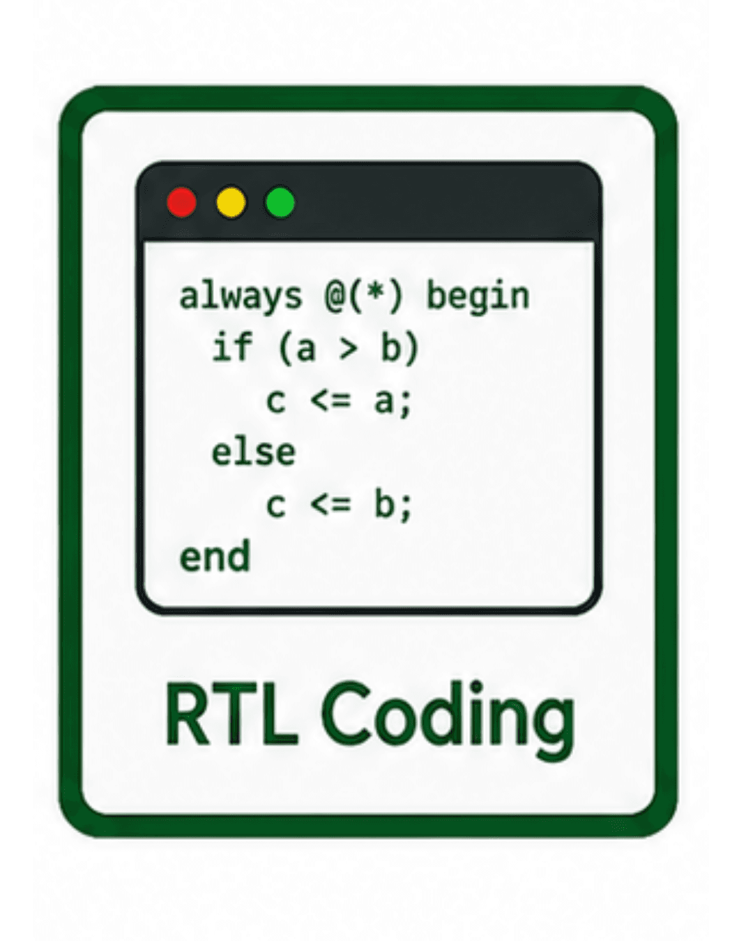
RTL Coding
Verilog / System Verilog
Lint & CDC
Testbench Writing
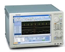
Logic Analyzers & Oscilloscopes
Available Course Schedules
Select a schedule that works best for you
Starts
03 Oct 2026
Time
09:30 AM – 12:30 PM
Duration
6 Months
Starts
05 Oct 2026
Time
07:00 AM – 09:00 AM
Duration
6 Months
Starts
10 Oct 2026
Time
02:00 PM – 05:00 PM
Duration
6 Months
Starts
12 Oct 2026
Time
08:00 PM – 10:00 PM
Duration
6 Months
Need a custom schedule?
Our team will craft the perfect batch for you.
What Our Happy Students Say
Real Feedback from our candidates
What We Offer Beyond Courses
24/7 Support
Round-the-clock assistance
LinkedIn Profile
Professional profile building
Resume Writing
Expert resume crafting
Alumni Guidance
Mentorship from graduates
Interview Prep
Mock interviews & tips
Live Projects
Real-world experience
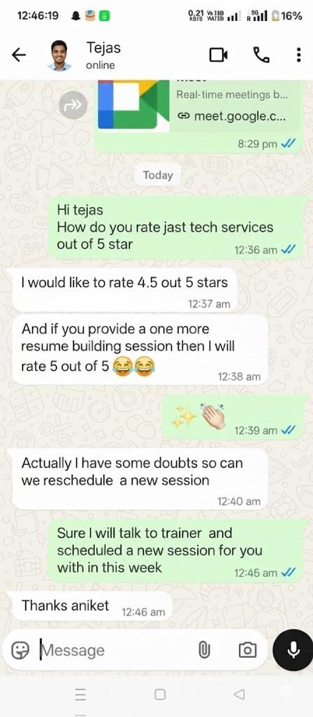
Tejas Kumar
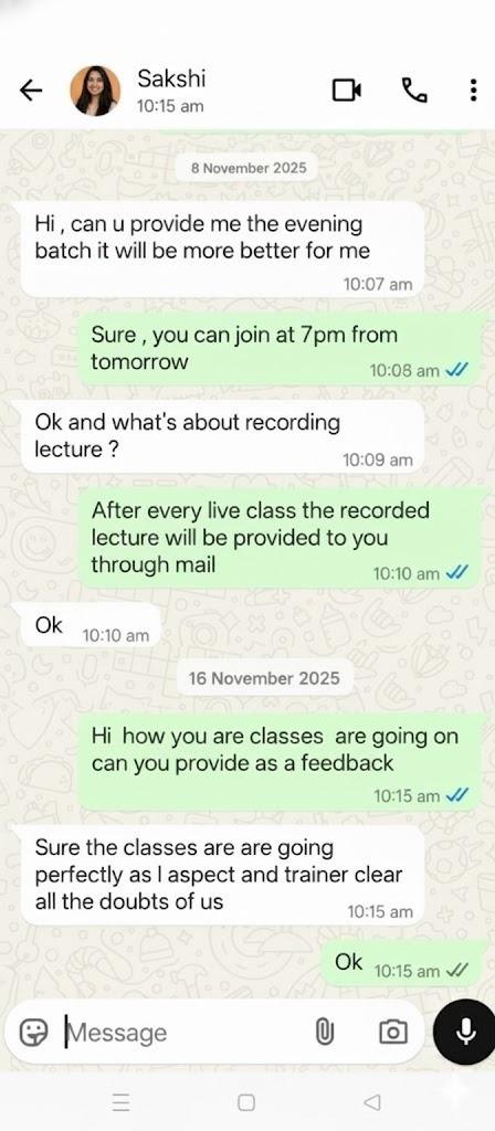
Sakshi Singh
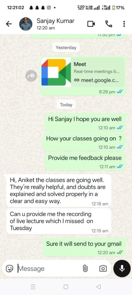
Sanjay Patel
Specialized Training Programs
JastTech For Corporates
JastTech Courses
Why JastTech is best VLSI Training institute in Noida
See how we stand out from the competition
Industry-focused curriculum covering RTL Design, Verification, FPGA, Physical Design, DFT, and Post-Silicon Validation. Our VLSI training institute in Noida aligns with current semiconductor industry requirements.
Course content may not be updated regularly with evolving VLSI technologies and industry standards.
Extensive lab sessions, simulation exercises, and real-world projects help students build practical VLSI design and verification skills.
Learning may focus more on theory with limited exposure to practical implementation.
Learn from experienced VLSI professionals with strong industry backgrounds and hands-on project expertise.
Trainers may have limited exposure to current semiconductor design and validation projects.
Work on industry-inspired projects that strengthen RTL coding, debugging, verification, and chip development skills.
Fewer opportunities to gain hands-on experience through structured projects.
Regular assignments, quizzes, coding exercises, and evaluations reinforce concepts and measure progress effectively.
Assessments may be less frequent and provide limited performance feedback.
Resume building, mock interviews, placement assistance, and career mentoring prepare students for VLSI job opportunities in Noida and across India.
Career guidance and placement support may be limited or unavailable.
Dedicated mentors provide personalized guidance and timely doubt resolution throughout the course.
Delayed responses and limited instructor availability can slow learning progress.
Industry-recognized certification validating practical VLSI skills and real-world project experience.
Certifications may offer less industry relevance and practical recognition.
Access course recordings, study materials, project files, and updated resources for continuous learning.
Learning resources may have restricted access after course completion.
Affordable training with practical exposure, career support, and industry-ready projects for maximum value.
Higher fees may not always include comprehensive learning resources or placement support.
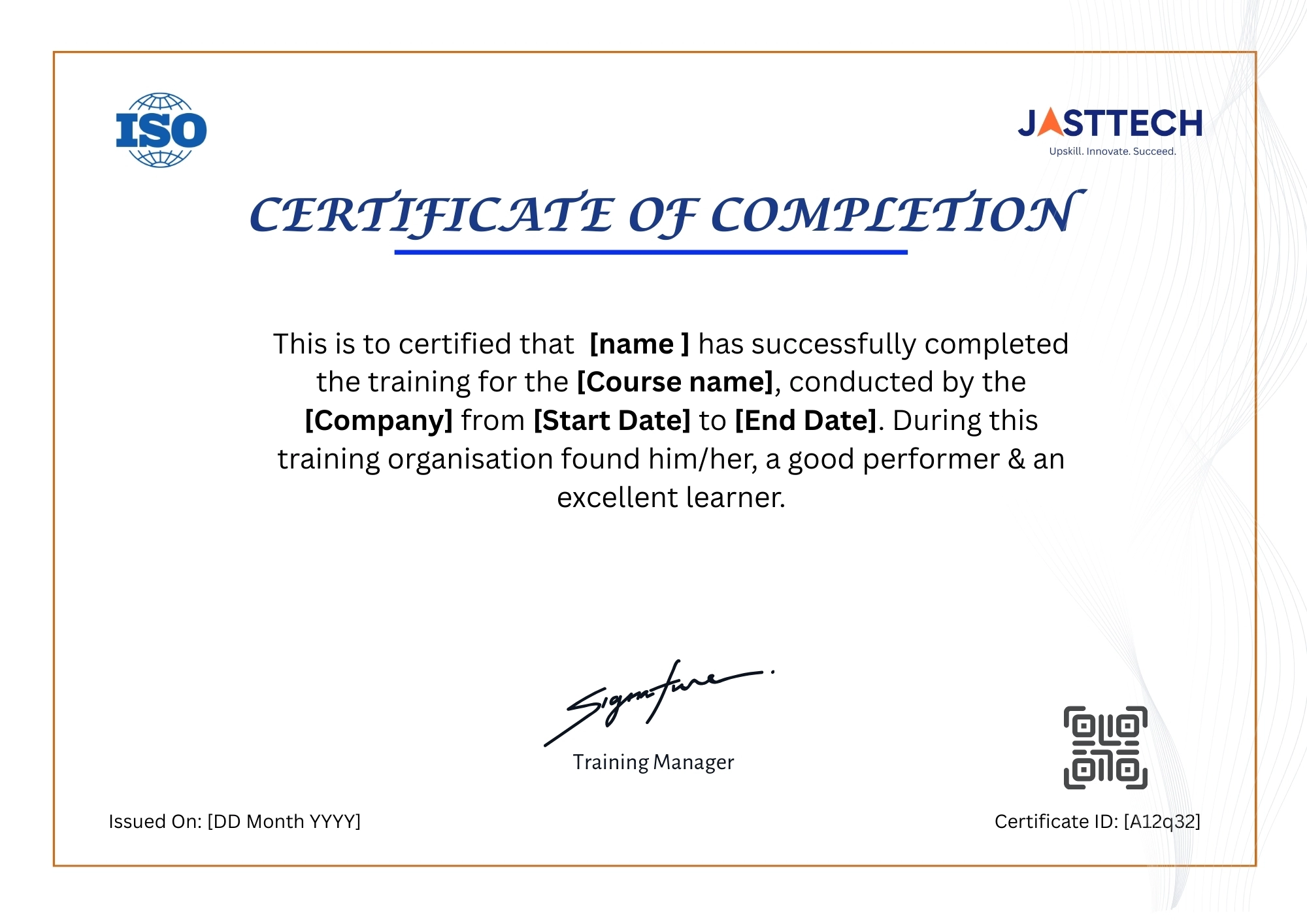
JastTech VLSI Training Institute Certificate
Prepare
Interview FAQ For VLSI Candidates
Curated questions with expert answers to help you ace your next interview.
Why do we use synchronous resets over asynchronous resets in sequential cells?
Synchronous resets are highly predictable because they only trigger on the active clock edge. This completely eliminates filtering glitches and timing race conditions, yielding simpler, clean circuit synthesis results across standard EDA routing trees.
How would you debug a failing test case in UVM environment?
I would check the scoreboard mismatches, monitor logs, sequence execution flow, and compare expected vs actual transactions step-by-step.
Your FPGA design works in simulation but not on hardware. What steps will you take?
I will check constraints file, clock settings, pin mapping, and hardware timing issues.
At which stage would you fix power optimization issues?
During synthesis and physical design stages using power-aware constraints and optimization techniques.
What happens if scoreboard is not matching expected results?
It indicates mismatch in DUT behavior, incorrect reference model, or transaction alignment issues.
Support
FAQs About Our VLSI Training Institute in Noida
Can't find what you're looking for? Reach out to our support team anytime.
What is the fee structure and duration for VLSI training in Noida?
Professional VLSI training in Noida at Jasttech ranges between ₹45,000 and ₹65,000, depending on whether you choose a short-term module (3 months) or a full job-oriented master track (6 months).
What subjects and modules are covered at our VLSI training institute in Noida?
As a premier VLSI training institute in Noida, Jasttech covers fundamental to advanced semiconductor tracks, including RTL Design, SystemVerilog & UVM Verification, Physical Design (STA & PnR), DFT, and FPGA Prototyping.
Why is Jasttech recognized among the best VLSI coaching centres in Noida?
Jasttech stands out among the best VLSI coaching centres in Noida due to our 10+ year industry-veteran trainers, real-world capstone projects, 0% EMI fee options, and dedicated placement support across Delhi NCR.
What average starting salary can freshers expect after course completion?
Entry-level chip design and verification engineers in the Noida region typically secure starting packages ranging from ₹5 LPA to ₹11 LPA, depending on interview performance and capstone project depth.
How does Jasttech handle placement support for semiconductor jobs?
We provide 100% placement assistance, including 1-on-1 technical mock interviews, resume optimization, and direct hiring drives with top electronic manufacturing and chip design companies located across Noida, Gurgaon, and Delhi NCR.
The support team was very cooperative and responsive. They made sure all doubts were cleared without delay. Great experience overall.
I had a great experience with the RF Circuit Design course. Thanks to the teaching staff for such a well planned and structured curriculum it really helped me clear my technical certification for my job.
I enrolled in the Post-Silicon Validation Certification Training at JastTech and found it quite different from typical courses. They focus on debugging techniques and real chip-level scenarios, which gave me a better idea of how things work.
One thing I really liked about the Data Analyst course at JastTech is their focus on consistency. Regular sessions and tasks help you stay on track and build a daily learning habit. Also, they provide recordings after live sessions, which help in revision.
I joined JastTech for the DFT course a few months back. At first, I wasn’t sure what to expect, but the classes turned out to be really helpful. The teaching is simple and not too complicated, which helped me keep up.
Take the Next Step in Your Career
Join thousands of learners who have upgraded their skills with our industry-focused training programs. Our experts are here to guide you every step of the way.
Related Articles & Insights
Deep dive into VLSI training institute in Noida with our expert-curated technical guides and industry updates.

Guidewire Configuration vs Integration: Which Career Path Should Beginners Choose?
Confused between Guidewire Configuration and Integration? Discover the responsibilities, skills, learning roadmap, practical projects, and modern cloud technologies beginners should understand before choosing a Guidewire career path in 2026.

Guidewire PolicyCenter Roadmap for Beginners: Complete Guide to Learning PolicyCenter Step by Step
Ever wondered what it actually takes to learn Guidewire PolicyCenter from scratch? This step-by-step roadmap breaks down exactly where to start, what skills matter most, and how to go from beginner to job-ready.

Guidewire Data Architecture Explained A Complete Beginner Guide 2026
Understand Guidewire data architecture from the ground up. This beginner-friendly 2026 guide explains entities, relationships, typelists, extensions, persistence, queries, Cloud APIs, integrations, and the practical architecture concepts needed for modern Guidewire development.

Why Should Software Engineers Learn Guidewire in India Before Switching Their Career
Thinking about a career switch? Discover why more software engineers are choosing a guidewire course in India to break into one of tech's most in-demand, best-paying niches — insurance technology.
We're Here to Help –
Reach Our Global Offices
Hyderabad
JastTech
Training & Development Center
91 Springboard Business Hub ,Madhapur LVS Arcade, 71, Jubilee Enclave, HITEC City, Hyderabad,India Telangana 500081
Pune
JastTech
Training & Development Center
Sr. No. 30/2/1, 3rd Floor, Above Rajrshi Shahu Bank & BOB Balaji Nagar, Dhankawadi, Katraj, Pune, Maharashtra 411043
Noida
JastTech
Training & Development Center
B 8, B Block, Sector 2, Noida, Metro Station Rd, near sector 15 Metro, Uttar Pradesh 201301
Hyderabad
JastTech
Training & Development Center
91 Springboard Business Hub ,Madhapur LVS Arcade, 71, Jubilee Enclave, HITEC City, Hyderabad,India Telangana 500081
Pune
JastTech
Training & Development Center
Sr. No. 30/2/1, 3rd Floor, Above Rajrshi Shahu Bank & BOB Balaji Nagar, Dhankawadi, Katraj, Pune, Maharashtra 411043
Noida
JastTech
Training & Development Center
B 8, B Block, Sector 2, Noida, Metro Station Rd, near sector 15 Metro, Uttar Pradesh 201301
Can't find a JastTech location near you? Contact us for more information.