



Master chip design at JastTech, the best VLSI training institute in Bangalore. Learn RTL, UVM, and Physical Design on Cadence & Synopsys tools with 100% placement aid.
Level
Advanced
Duration
6 Months
Our Alumni Work At












JastTech is recognized as the best VLSI training institute in Bangalore, offering industry-aligned programs designed to bridge the gap between academic electronics engineering and modern silicon design houses. Our comprehensive curriculum provides deep-dive practical exposure to RTL design, ASIC flows, FPGA development, and advanced UVM verification methodologies.
Led by veteran chip architects with over 10 years of domain expertise, our VLSI training in Bangalore features rigorous hands-on labs utilizing production-grade EDA tools from Cadence and Synopsys. Whether you choose our adaptive live online modules or physical classrooms across Bangalore's premier technology corridors, you gain direct access to intensive career preparation. Backed by 5 real-world chip design projects and 150+ semiconductor hiring partners, we ensure you emerge placement-ready for top-tier hardware engineering
- VLSI Design Engineer
- RTL Design Engineer
- RTL Verification Engineer
- SoC Design Engineer
- Front-End VLSI Engineer
- Back-End VLSI Engineer
- Logic Design Engineer
- Chip Design Engineer
- Physical Verification Engineer
Best VLSI Training Institute in Bangalore Curriculum
Introduction to VLSI and Semiconductor Fundamentals
Learn the fundamentals of semiconductor technology, IC design flow, ASICs, FPGAs, and the VLSI industry ecosystem.
Digital Electronics Fundamentals
Understand digital logic design concepts including combinational circuits, sequential circuits, flip-flops, counters, and FSMs.
Verilog HDL Programming
Master Verilog HDL for designing, modeling, simulating, and testing digital hardware systems efficiently.
SystemVerilog for Design and Verification
Learn SystemVerilog features for advanced RTL design, assertions, functional coverage, and verification methodologies.
RTL Design Methodology
Develop industry-standard RTL coding skills for creating synthesizable, optimized, and scalable digital designs.
Related Courses
Training Roadmap
Seven intentional milestones — from first session to dream job.
Onboarding
- Meet your industry mentor
- Define your goals
- Skill gap assessment
Core Learning
- Live interactive classes
- AI-curated content
- Recorded sessions
Hands-on Practice
- Weekly assignments
- MCQ evaluations
- Module quizzes
Real Projects
- 3 live industry projects
- Portfolio building
- Case studies
Mentorship
- 1:1 doubt sessions
- Peer collaboration
- Expert feedback
Certification
- Exam preparation
- Practice dumps
- Industry-recognised certificate
Career Launch
- Resume crafting
- Mock interviews
- Job placement support
Industry Projects You Build at JastTech VLSI Training Institute in Bangalore
Skills and Tools You Will Learn
Verdi
Saleae Logic Analyzer
JTAG / OpenOCD
Wireshark
FPGA Prototyping
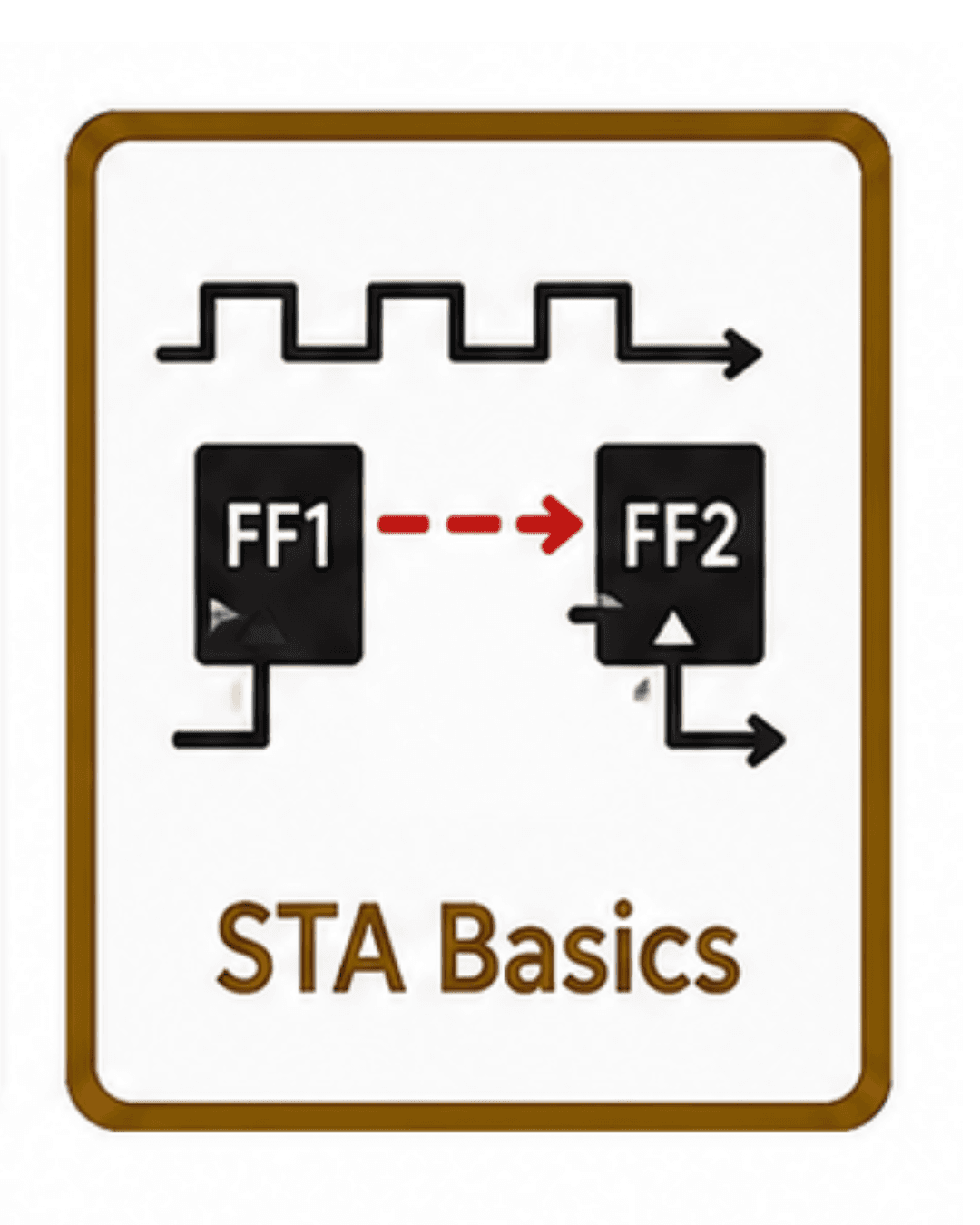
STA Basics
Vivado
Oscilloscope tools
Available Course Schedules
Select a schedule that works best for you
Starts
24 Oct 2026
Time
09:30 AM – 12:30 PM
Duration
6 Months
Starts
26 Oct 2026
Time
07:00 AM – 09:00 AM
Duration
6 Months
Starts
31 Oct 2026
Time
02:00 PM – 05:00 PM
Duration
6 Months
Starts
02 Nov 2026
Time
08:00 PM – 10:00 PM
Duration
6 Months
Need a custom schedule?
Our team will craft the perfect batch for you.
What Our Happy Students Say
Real Feedback from our candidates
What We Offer Beyond Courses
24/7 Support
Round-the-clock assistance
LinkedIn Profile
Professional profile building
Resume Writing
Expert resume crafting
Alumni Guidance
Mentorship from graduates
Interview Prep
Mock interviews & tips
Live Projects
Real-world experience
What Our Happy Students Say
Real Feedback from our candidates
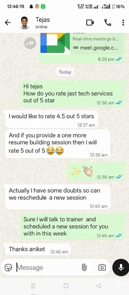
Tejas D.
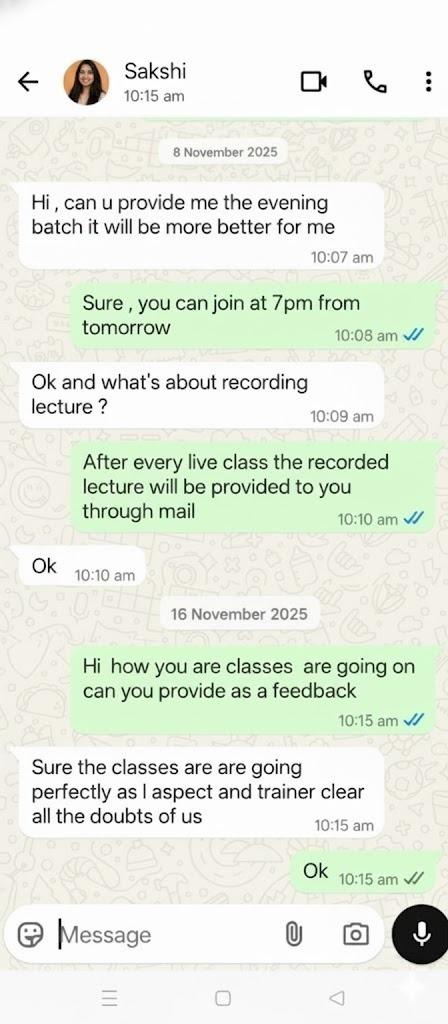
Sakshi
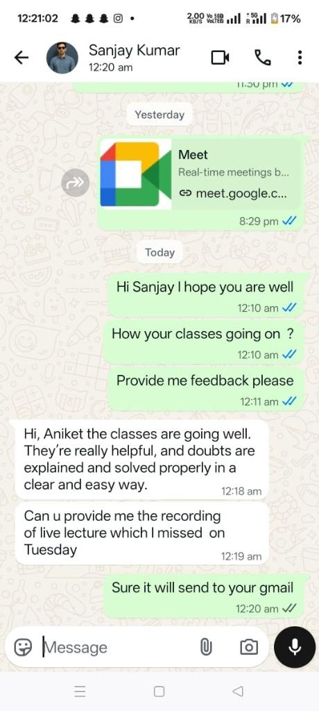
Sanjay Kumar
Specialized Training Programs
JastTech For Corporates
JastTech Courses
Why JastTech is Best VLSI Training Institute in Bangalore ?
See how we stand out from the competition
Our VLSI Training Institute in Bangalore offers an industry-aligned curriculum covering RTL Design, Verification, FPGA, ASIC, Physical Design, and Post-Silicon Validation with practical applications.
Course content may be outdated or lack coverage of the latest semiconductor technologies.
Students gain real-world experience through live labs, simulation exercises, and project-based learning to build job-ready VLSI skills.
Practical sessions may be limited, with a stronger focus on theory than implementation.
Learn from experienced VLSI professionals with hands-on industry knowledge, mentorship, and guidance on current design and verification practices.
Faculty may have limited exposure to live semiconductor projects and industry workflows.
Work on chip design, RTL coding, verification, and debugging projects that reflect real semiconductor development environments.
Students may have fewer opportunities to participate in practical, industry-style projects.
Regular assignments, coding exercises, quizzes, and technical evaluations help reinforce concepts and improve problem-solving skills.
Assessments may be infrequent and provide limited opportunities for continuous improvement.
Resume building, interview preparation, mock interviews, and placement guidance help learners prepare for VLSI job opportunities in Bangalore and beyond.
Career assistance may be basic or unavailable after course completion.
Dedicated mentors provide timely doubt resolution and one-on-one guidance throughout the learning journey.
Delayed responses and limited mentor availability can slow learning progress.
Earn an industry-recognized certification that validates your practical VLSI skills and strengthens your professional profile.
Certifications may have limited industry recognition or practical relevance.
Get lifetime access to recorded sessions, study materials, and updated resources to continue learning at your own pace.
Learning resources may expire or require additional payment after course completion.
JastTech provides high-quality VLSI training in Bangalore at competitive fees, offering excellent value with practical exposure and career support.
Higher fees may not include project work, updated content, or placement assistance.
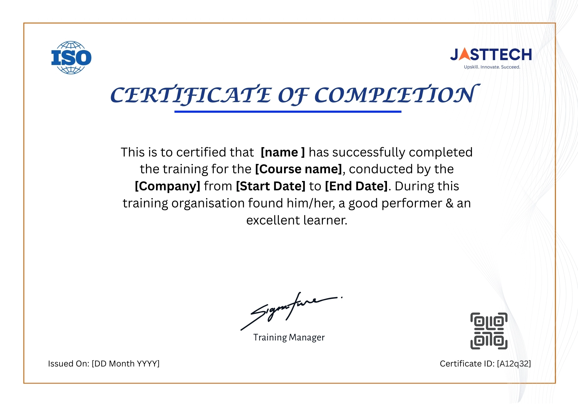
JastTech VLSI Training Institute Certificate
Prepare
Most Asked VLSI Interview Questions
Curated questions with expert answers to help you ace your next interview.
What is the difference between an ASIC and an FPGA design flow?
An ASIC is a custom integrated circuit designed for a specific application that cannot be altered or reprogrammed after fabrication, offering maximum performance and low power consumption for high-volume production. An FPGA contains configurable logic blocks that can be reprogrammed multiple times post-manufacturing, making it ideal for rapid prototyping and hardware debugging without high manufacturing costs.
Explain setup time and hold time violations in Static Timing Analysis. How do you fix them?
Setup time is the minimum time data must remain stable before the active clock edge, and violations occur when the data path delay is too long. They are fixed by reducing combinational logic delay or inserting pipelines. Hold time is the minimum time data must remain stable after the clock edge, and violations occur when the data path delay is too short. They are fixed by inserting delay buffers into the data path.
What causes a latch to be unintendedly inferred in Verilog RTL design, and how do you prevent it?
Unintended latches are inferred when a combinational always block fails to specify an output value for all possible execution paths. This typically happens if an if statement lacks an else block or a case statement misses a default assignment. You can prevent latch inference by assigning default values to all outputs at the beginning of the combinational block.
What is Clock Domain Crossing and how do you prevent metastability in multi-clock SoCs?
Clock Domain Crossing occurs when a signal travels between asynchronous clock domains. If the transition happens inside the setup or hold window of the destination register, it causes metastability. To prevent this, single-bit signals must use multi-stage synchronizers, while multi-bit data paths require asynchronous FIFOs with Gray-coded pointers or handshaking protocols.
What is the difference between blocking and non-blocking assignments in Verilog?
Blocking assignments use the equal sign and execute sequentially within an always block, preventing subsequent statements from running until the current one finishes. They are primarily used to model combinational logic. Non-blocking assignments use the less than equal sign and execute concurrently, meaning all evaluations happen at the same time before updating the variables. They are used exclusively to model sequential logic to avoid simulation race conditions.
Support
FAQs About Our VLSI Training Institute
Can't find what you're looking for? Reach out to our support team anytime.
Why is JastTech considered the best VLSI training institute in Bangalore?
JastTech stands out by offering an industry-aligned learning experience engineered for core engineering roles. Students work directly with production-grade EDA toolchains from Synopsys and Cadence, guided by senior chip architects with over a decade of domain experience. Our comprehensive curriculum, matched with dedicated placement engineering, makes us the preferred choice for launching a successful semiconductor career.
What core topics are covered in the VLSI training in Bangalore at JastTech?
Our curriculum provides extensive practical coverage across both front-end and back-end domains. Key subjects include Advanced Digital Design, synthesizable Verilog and SystemVerilog HDL, Functional Verification using UVM architecture, FPGA deployment, ASIC design flows, Static Timing Analysis, and Design for Testability.
What job opportunities are open after completing this chip design course?
Graduates are prepared for specialized entry-level engineering roles across major semiconductor houses. Typical career paths include Junior RTL Design Engineer, Functional Verification Engineer, ASIC Implementation Associate, Physical Design Trainee, FPGA Developer, and Static Timing Analysis Engineer.
Who is eligible to enroll in JastTech's VLSI training program?
This advanced course is tailored for engineering graduates and postgraduates, specifically B.E., B.Tech, and M.Tech students from Electronics and Communication, Electrical Engineering, and Instrumentation streams. It is also ideal for embedded systems professionals looking to transition directly into hardware design.
Does the VLSI course at JastTech include physical lab access to licensed EDA tools?
Yes, our training features extensive practical lab sessions where students gain hands-on access to industry-standard toolchains from Synopsys and Cadence. Learning on production-grade software ensures that your technical engineering skills match the exact workflow requirements of real semiconductor design houses.
The support team was very cooperative and responsive. They made sure all doubts were cleared without delay. Great experience overall.
I had a great experience with the RF Circuit Design course. Thanks to the teaching staff for such a well planned and structured curriculum it really helped me clear my technical certification for my job.
I enrolled in the Post-Silicon Validation Certification Training at JastTech and found it quite different from typical courses. They focus on debugging techniques and real chip-level scenarios, which gave me a better idea of how things work.
One thing I really liked about the Data Analyst course at JastTech is their focus on consistency. Regular sessions and tasks help you stay on track and build a daily learning habit. Also, they provide recordings after live sessions, which help in revision.
I joined JastTech for the DFT course a few months back. At first, I wasn’t sure what to expect, but the classes turned out to be really helpful. The teaching is simple and not too complicated, which helped me keep up.
Take the Next Step in Your Career
Join thousands of learners who have upgraded their skills with our industry-focused training programs. Our experts are here to guide you every step of the way.
Related Articles & Insights
Deep dive into Best VLSI Training Institute in Bangalore with our expert-curated technical guides and industry updates.

RTL Design and Verification Training in India: Why It Is the Top Career Choice in 2026
Discover why RTL Design and Verification Training in India is the top career choice in 2026. Learn about industry demand, essential skills, career opportunities, salaries, and placement prospects.

Top 10 VLSI Training Institutes in India with Placement Assistance
Explore the top 10 VLSI training institutes in India with placement assistance. Compare courses, hands-on projects, expert trainers, certifications, and career support to choose the right institute.

From ASIC to FPGA: Exploring Specialized VLSI Job Profiles
Explore ASIC & FPGA VLSI Career Paths

DFT vs Functional Testing in VLSI What's the Difference?
Confused about DFT and functional testing in VLSI? Discover how scan chains, ATPG, fault models, functional tests, and manufacturing testing work together to identify defects and ensure reliable silicon.
We're Here to Help –
Reach Our Global Offices
Hyderabad
JastTech
Training & Development Center
91 Springboard Business Hub ,Madhapur LVS Arcade, 71, Jubilee Enclave, HITEC City, Hyderabad,India Telangana 500081
Pune
JastTech
Training & Development Center
Sr. No. 30/2/1, 3rd Floor, Above Rajrshi Shahu Bank & BOB Balaji Nagar, Dhankawadi, Katraj, Pune, Maharashtra 411043
Noida
JastTech
Training & Development Center
B 8, B Block, Sector 2, Noida, Metro Station Rd, near sector 15 Metro, Uttar Pradesh 201301
Hyderabad
JastTech
Training & Development Center
91 Springboard Business Hub ,Madhapur LVS Arcade, 71, Jubilee Enclave, HITEC City, Hyderabad,India Telangana 500081
Pune
JastTech
Training & Development Center
Sr. No. 30/2/1, 3rd Floor, Above Rajrshi Shahu Bank & BOB Balaji Nagar, Dhankawadi, Katraj, Pune, Maharashtra 411043
Noida
JastTech
Training & Development Center
B 8, B Block, Sector 2, Noida, Metro Station Rd, near sector 15 Metro, Uttar Pradesh 201301
Can't find a JastTech location near you? Contact us for more information.