

How to Choose the Best Post-Silicon Validation Training Institute in India
Navigate through this article using the table of contents below
Table of Contents
No headings found in this article.
Post-silicon validation is one of the most in-demand skills in the Indian semiconductor industry right now. Companies like Intel, Qualcomm, AMD, and Renesas are actively hiring for it, the salaries at entry level are above most other VLSI tracks, and the number of trained engineers available is nowhere near enough to meet the demand. So the decision to learn post-silicon validation is usually not the hard part. The hard part is figuring out which training institute will actually prepare you for the job — and which ones are just selling you a certificate.
This blog is a practical guide to making that decision correctly. Not a list of marketing claims. A real breakdown of what matters, what to ignore, and what questions to ask before you spend your time and money anywhere.
Understand What Post-Silicon Validation Actually Demands Before You Choose Anywhere
Most people make the mistake of comparing training institutes before they fully understand what post-silicon validation as a career actually requires from an engineer. That order of thinking leads to picking a program based on price, location, or a website that looks credible — without ever asking whether the training matches the reality of the job.
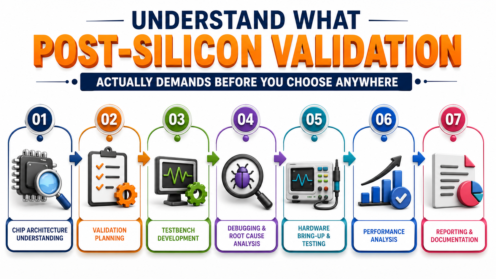
Post-silicon validation is the process of testing a chip after it has been physically manufactured. Not in simulation. On real silicon, in real conditions, with real failures that nobody in the design team predicted. The engineer doing this work needs to understand how chips behave under actual voltage and temperature variation, how to access a chip's internal state through debug interfaces, how to interpret signals from high-speed interfaces at multi-gigabit speeds, and how to trace a failure back to its exact root cause through a systematic process of elimination. That is a very specific combination of hardware knowledge, software skills, and analytical thinking — and not every training program is built to develop all three.
Before comparing any institutes, write down what the job actually requires. Look at five or six post-silicon validation job descriptions posted by Intel, Qualcomm, AMD, or Renesas in India. Note which skills appear consistently across all of them. That list — not any institute's marketing material — is your benchmark. Every training program you evaluate should be held against it. The ones that cover those skills with genuine depth are worth your attention. The ones that list the keywords but cannot show you how they teach them are not.
The Trainer's Background Matters More Than the Institute's Name
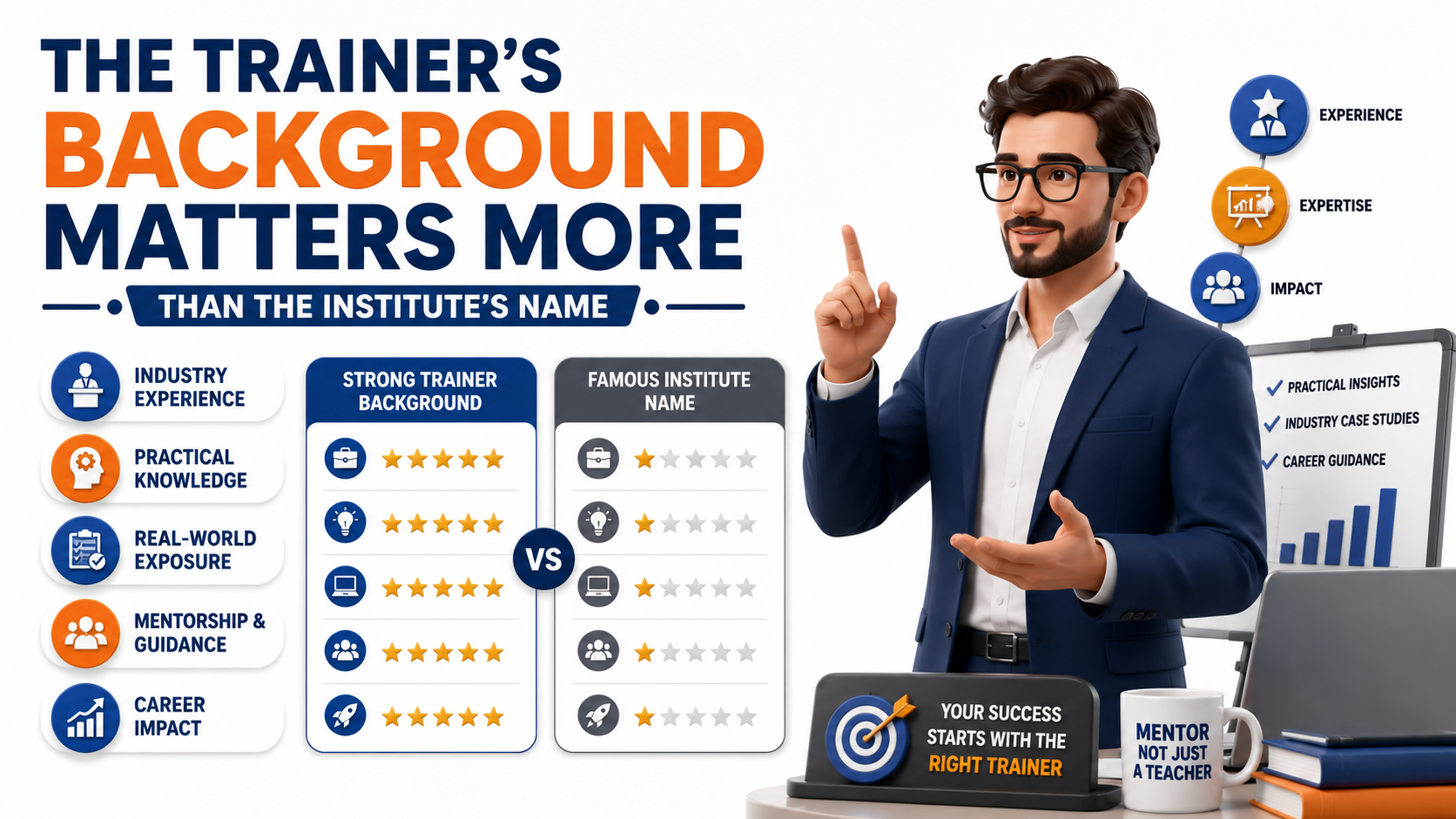
A training institute is ultimately only as good as the person teaching you. In post-silicon validation specifically, this matters more than in almost any other VLSI track — because the real knowledge in this field is not in textbooks. It lives in the experience of someone who has powered up a chip that refused to boot, isolated a failure to a specific power rail at 3am, and walked a silicon bug back to a root cause through a combination of instruments and systematic thinking.
Ask every trainer you consider a direct question: which semiconductor company did you work at, on which chip program, and what was your role? A trainer who has personally run silicon bring-up on a real SoC at a company like Intel or Qualcomm will teach you things that no amount of theoretical curriculum can cover. A trainer who has only taught without working in the industry will give you vocabulary without substance.
This is not a harsh standard. It is a fair one. You are preparing for a role where the hiring manager will ask you to walk through a real debug scenario in the interview. Your trainer needs to have done that themselves.
Look for the curriculum which suit for your job

Most training institutes publish a curriculum. On the surface, many of them look similar — silicon bring-up, JTAG, lab instruments, protocol testing. The difference is in what is actually covered at depth versus what is listed as a topic heading and then glossed over in two slides.
A curriculum that will genuinely prepare you for a post-silicon validation role should cover the following areas with real depth:
• Silicon bring-up methodology — the exact sequence for powering a chip for the first time, checking power rails, validating clock outputs, establishing JTAG access, and running an initial boot sequence. This should be practiced, not just described.
• Lab instrument operation — hands-on use of an oscilloscope to capture and interpret a real signal, set up a trigger, and measure parameters like rise time, jitter, and eye height. Not a demonstration. Your hands on the equipment.
• High-speed interface validation — how to test PCIe, DDR, USB, or Ethernet on actual silicon using protocol analyzers, and how to interpret what a protocol analyzer shows you when a link fails to train.
• Debug methodology — a structured framework for approaching a chip failure. This is not a tool skill. It is a way of thinking that separates engineers who find root causes from engineers who guess and check.
• Python for test automation — writing scripts that control lab instruments, run test sequences automatically, parse results, and generate reports. This appears on almost every validation job description in India.
When you review a curriculum, ask the institute how much time is spent on each of these areas. An post silicon validation training institute in india that spends eight hours on lab instruments across five weeks is not the same as one that spends eight hours on lab instruments in the first three days and builds on it throughout. Depth over breadth is what the job market rewards.
A Real Project Is Non-Negotiable — Know What That Actually Means
Almost every VLSI training program in India claims to include a project. In post-silicon validation, the word project is used to describe a very wide range of things — from watching a trainer demonstrate a bring-up sequence on camera, to actually connecting a hardware board yourself, writing your own test script, debugging a failure you introduced intentionally, and producing a test report based on your own results.
Only the second version prepares you for a job. In a post-silicon validation interview, you will be asked to describe your project in detail. What board did you work on? What was the chip? What test did you run? What failed? How did you debug it? What did you find? If your honest answer to any of those questions is 'I watched someone else do it,' you are in a difficult position.
Before enrolling, ask specifically: what is the project, what hardware does it involve, and what will I personally do versus what will the trainer demonstrate? A confident institute will give you a clear, specific answer. An institute that is vague about the project is usually vague about it for a reason.
Placement Support Should Be Specific, Not Aspirational
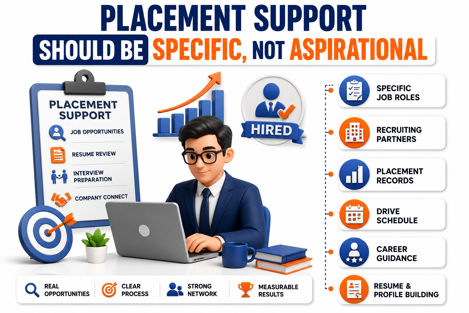
Placement support is the most over-promised and least-verified thing in the Indian training industry. Every institute offers it. The quality difference between what different institutes actually deliver is enormous.
There are two types of placement support. The first type is aspirational — the institute connects you to a job board, sends your resume to a list of companies, and calls it placement support. The second type is specific — the institute has relationships with actual hiring managers at semiconductor companies, runs mock technical interviews that simulate the real thing, and can point you to recent placed engineers you can speak with directly.
Here is a simple test: ask the institute to name three companies where engineers from the last two batches were placed in post-silicon validation roles specifically. Ask for the engineers' names or LinkedIn profiles so you can verify independently. If the institute responds confidently and clearly, the placement support is real. If the answer is vague, delayed, or deflected toward general VLSI placements rather than validation-specific ones, you have your answer.
Batch Size and Access Hours Tell You More Than the Fee
Two details that most candidates never ask about turn out to be among the most practically important: how many people are in each training batch, and how many hours of lab access do you get per week outside of class time.
Post-silicon validation is a skill that improves with repetition. The more time you spend operating instruments, running tests, and working through failures on your own, the more naturally the debug methodology becomes. A batch of five to eight engineers learning together with access to lab equipment outside scheduled class hours is a completely different learning environment from a batch of twenty-five watching a single demonstration. One produces engineers who can do the job. The other produces engineers who have attended the course.
Ask directly: what is the maximum batch size, and can I come in and use the lab outside of class hours? If the institute has a ratio problem — too many people, too few instrument stations — the training will be superficial regardless of how strong the curriculum looks on paper.
Conclusion
Choosing a post-silicon validation training institute is not a decision you should make based on a website, a brochure, or a phone call with an admissions coordinator. It is a decision you should make after visiting the lab, speaking directly with the trainer about their industry background, understanding exactly what the project involves, and verifying placement outcomes with engineers who have actually been placed. The institutes that can answer all of those questions clearly and confidently are the ones worth your time. JastTech post-silicon validation training is built on exactly these principles — ISO 9001:2015 certified, lab-based, and designed to produce engineers who are ready for the job from day one, across centers in Bangalore, Hyderabad, Chennai, Noida, Pune, and Kolkata.