

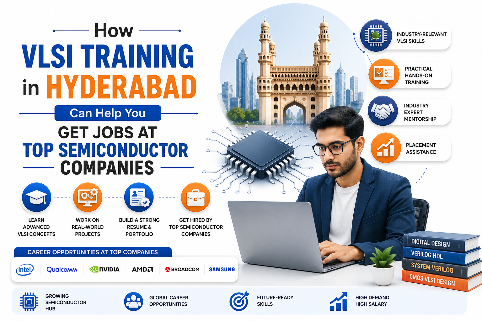
How VLSI Training in Hyderabad Can Help You Get Jobs at Top Semiconductor Companies
Navigate through this article using the table of contents below
Table of Contents
No headings found in this article.
There is a version of a VLSI career that most engineers imagine — working at Qualcomm or AMD, designing chips that go into the devices billions of people use every day. Then there is the reality of how most people try to get there: a degree, a few YouTube tutorials, and hope. The gap between those two things is exactly what the right VLSI training in Hyderabad is designed to close.
Hyderabad is no longer just a software city. It is now home to some of the most significant semiconductor operations in Asia — and the companies building those operations are actively looking for engineers who are trained, not just educated. This blog explains how training in Hyderabad specifically positions you to land those roles, and what makes the difference between a candidate who gets hired and one who keeps applying.
Hyderabad Semiconductor Ecosystem Is Now Too Big to Ignore
A few years ago, Hyderabad was a distant second to Bangalore in VLSI hiring conversations. That gap has closed significantly. Qualcomm's Hyderabad center is one of the company's largest engineering operations outside the US, with teams working on Snapdragon chip architecture, 5G modem design, and AI accelerator development. AMD runs a campus here that contributes directly to Ryzen and EPYC processor development — chips that compete at the highest level in the global market.
Apple operates a silicon design team in Hyderabad. Intel has a meaningful presence focused on FPGA and SoC development. NVIDIA, NXP, Renesas, Samsung Semiconductor, Cadence, and Synopsys all have active engineering teams here. And MosChip — India's first fabless semiconductor company — is headquartered right in Hyderabad.
Why the Right Training Matters More Than the Right Degree
Semiconductor companies in Hyderabad hire from IITs, NITs, and private colleges alike. What they do not hire based on is the name of the institution alone. A recruiter at Intel or Qualcomm cares about one thing more than your college: can you do the job from day one.
The problem is that most engineering programs — even good ones — do not go deep enough into the tools and workflows that these companies actually use. A student can complete four years of ECE and still never open Synopsys VCS, never write a UVM testbench from scratch, never trace a timing path through a real design. The knowledge gap is not a character flaw — it is a curriculum gap. And it is exactly what specialized VLSI training is designed to fill.
Engineers who come into interviews having genuinely used industry-standard EDA tools, who can walk through a real project they built themselves, and who understand how to approach a design problem or a debug scenario systematically — these are the candidates who get offers. The degree opened the door. The training is what got them through it.
What Top Semiconductor Companies Actually Look for in VLSI Interviews
Understanding what companies like Qualcomm, AMD, and Intel actually test in interviews is one of the most useful things you can know before you start training — because it tells you exactly what your training needs to build.
For RTL Design roles, interviews test whether you can write Verilog or SystemVerilog for a real problem, not just explain what RTL means. Interviewers ask you to code a FIFO, a state machine, or an arbiter on the spot, then ask questions about timing, reset, and edge cases. For Verification roles, the focus shifts to UVM — can you describe the architecture of a testbench you built, explain how your coverage plan was structured, and walk through how you debugged a failing test? For Physical Design, interviewers want to know how you approached a timing closure problem, what congestion looked like in your design and how you resolved it.
Across all tracks, the questions that consistently separate strong candidates from weak ones are the practical ones — not the theoretical definitions, but the real decision-making. That kind of confident, specific answer only comes from having actually done the work during training, not from having read about it.
What a VLSI Course With Placement Support Actually Looks Like
Placement support is one of the most over-promised things in the training industry. Every institute claims to offer it. What most people do not realize is that placement support has a very wide range — from sending your resume to a generic mailing list, all the way to structured mock interviews, direct referrals to hiring managers, and active follow-up until you are placed.
A VLSI course with placement that is actually worth the name does a few specific things. It runs technical mock interviews that simulate what Qualcomm or Intel actually ask — not generic HR rounds. It prepares you to talk through your project confidently and in detail, because that project discussion is often the deciding factor in an interview. It has existing relationships with semiconductor companies in Hyderabad, so when your batch is ready, there is a direct channel to present you rather than your resume going into a cold portal.
The questions to ask before enrolling in any program: how many engineers from the last two batches were placed, at which companies, and in which specific roles? An institute with real placement outcomes answers this clearly. One that deflects with percentages and vague references to 'industry connections' is telling you something important without saying it directly.
• Ask for names of recently placed engineers and verify them on LinkedIn.
• Confirm whether mock interviews are conducted by working industry professionals or just by in-house trainers.
• Check whether placement support covers the specific track you are training for — not just general VLSI placements.
JastTech offers a VLSI course with placement support across all six centers including Hyderabad, with mock technical interviews, direct industry connections, and dedicated support until placement — not just until the course ends.
How to Use Hyderabad's Geography to Your Advantage During and After Training
One thing that experienced Hyderabad engineers know — and that most people starting out miss — is that the semiconductor industry in this city is geographically tight. HITEC City, Madhapur, Gachibowli, and Kondapur sit within a few kilometers of each other. Qualcomm, AMD, Intel, Apple's silicon team, Synopsys, and Cadence are all clustered in this corridor. That density creates opportunities that people in other cities simply do not have access to.
During training, this matters because walk-in drives and technical events organized by these companies happen locally. IEEE Hyderabad Section runs technical seminars. Alumni from training batches who now work at AMD or Qualcomm are often willing to meet for a coffee and share what the interview process actually looked like. These are not small advantages — in a competitive market, a referral or an insider view of the interview format can shift the outcome.
Conclusion
Hyderabad has built a semiconductor ecosystem that is real, growing, and actively hiring. The engineers who enter it successfully are not the ones with the best degrees — they are the ones with the best preparation. Training in the right place, with the right curriculum and genuine placement support, is what converts ambition into an offer letter.