

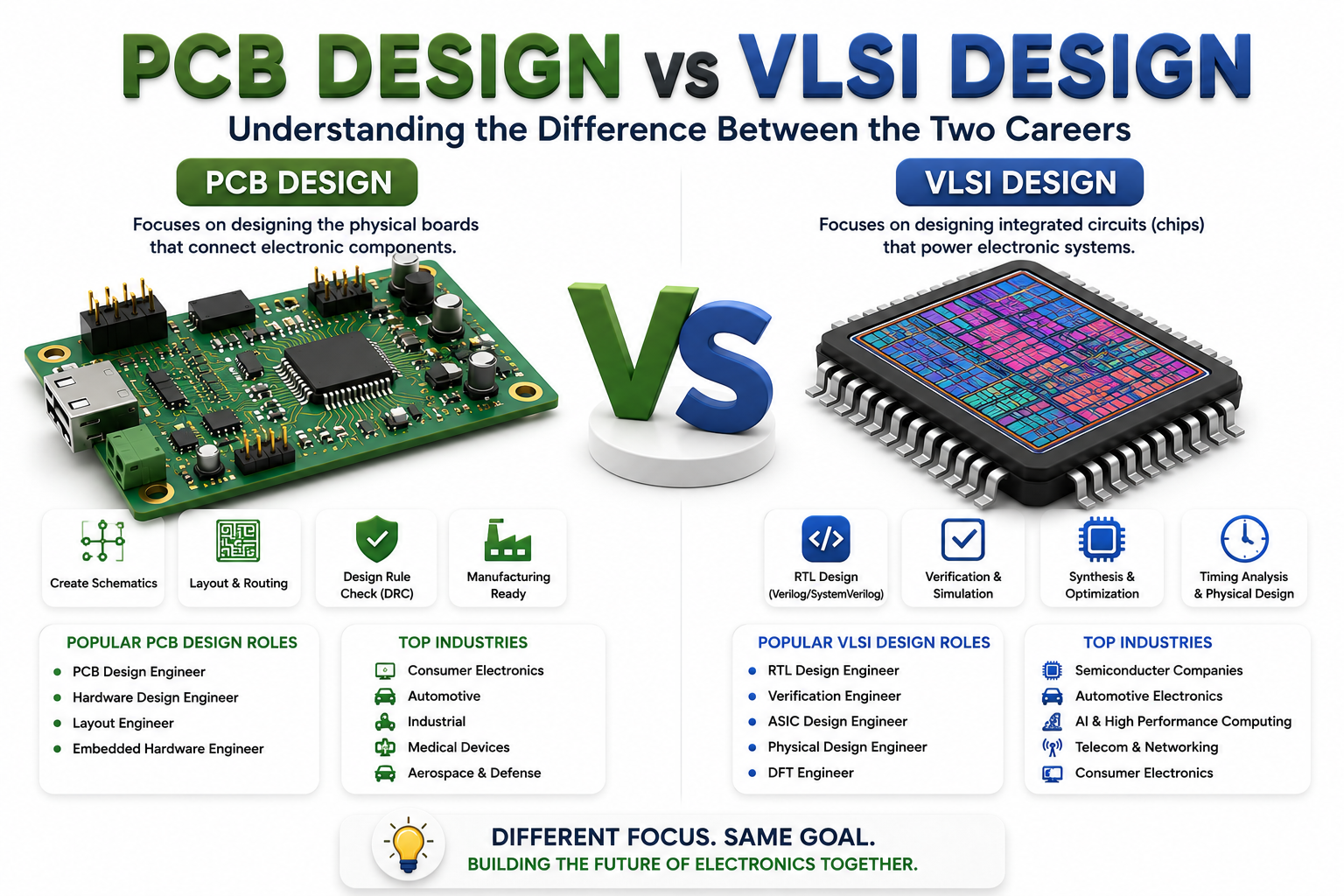
PCB Design vs VLSI Design: Understanding the Difference Between the Two Careers
Navigate through this article using the table of contents below
Table of Contents
No headings found in this article.
The semiconductor industry is expanding faster than ever, creating exciting opportunities for electronics engineers. But one question continues to confuse students and fresh graduates: should you choose PCB Design or VLSI Design as your career? Although both fields are essential to modern electronics, they differ significantly in skills, tools, career paths, and growth opportunities.
Choosing the right specialization can shape your future in the electronics industry. This guide explains the differences between PCB Design and VLSI Design, compares career prospects, salaries, required skills, and industry demand, helping you make an informed decision while preparing for a successful engineering career.
PCB Design vs VLSI Design: Understanding the Core Difference
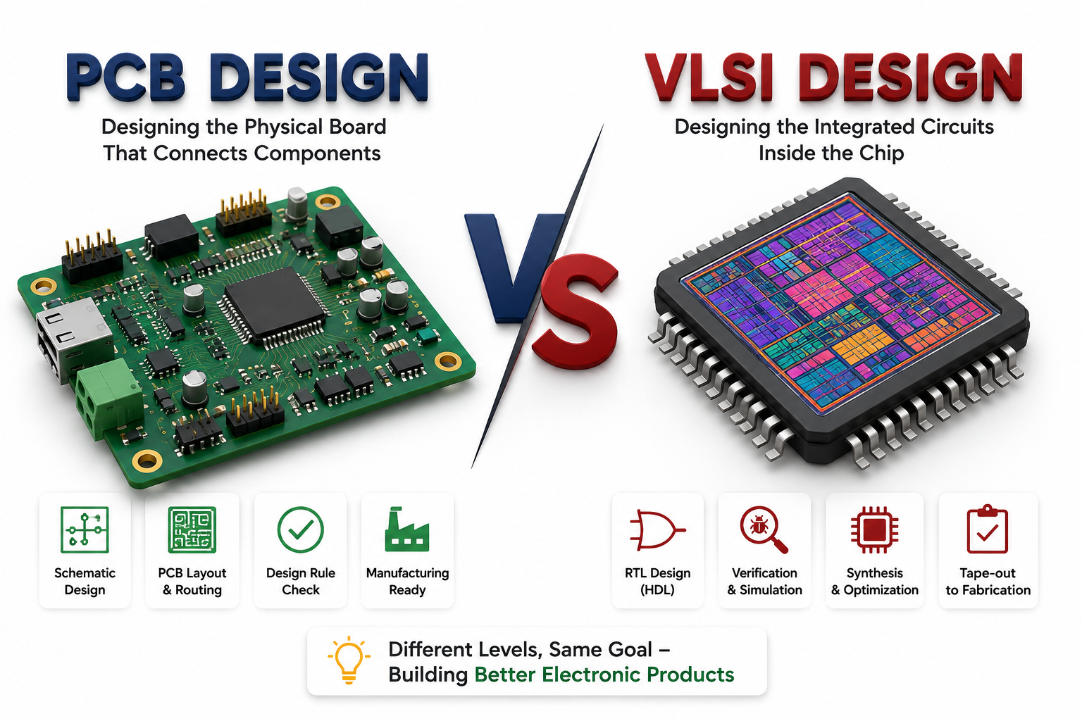
PCB (Printed Circuit Board) Design focuses on designing the physical boards that connect electronic components. PCB designers create schematics, place components, route signals, and ensure the board meets electrical and manufacturing requirements. Their work is essential in consumer electronics, automotive systems, medical devices, industrial automation, and IoT products.
VLSI (Very Large Scale Integration) Design, on the other hand, involves designing integrated circuits (ICs) containing millions or even billions of transistors on a single silicon chip. VLSI engineers work on digital logic, RTL coding, verification, synthesis, physical design, timing analysis, and chip validation before fabrication.
Both careers contribute to building electronic products, but they operate at different levels of hardware development. While PCB Design connects existing components, VLSI Design creates the chips that power those components.
Skills, Software, and Technical Knowledge Required
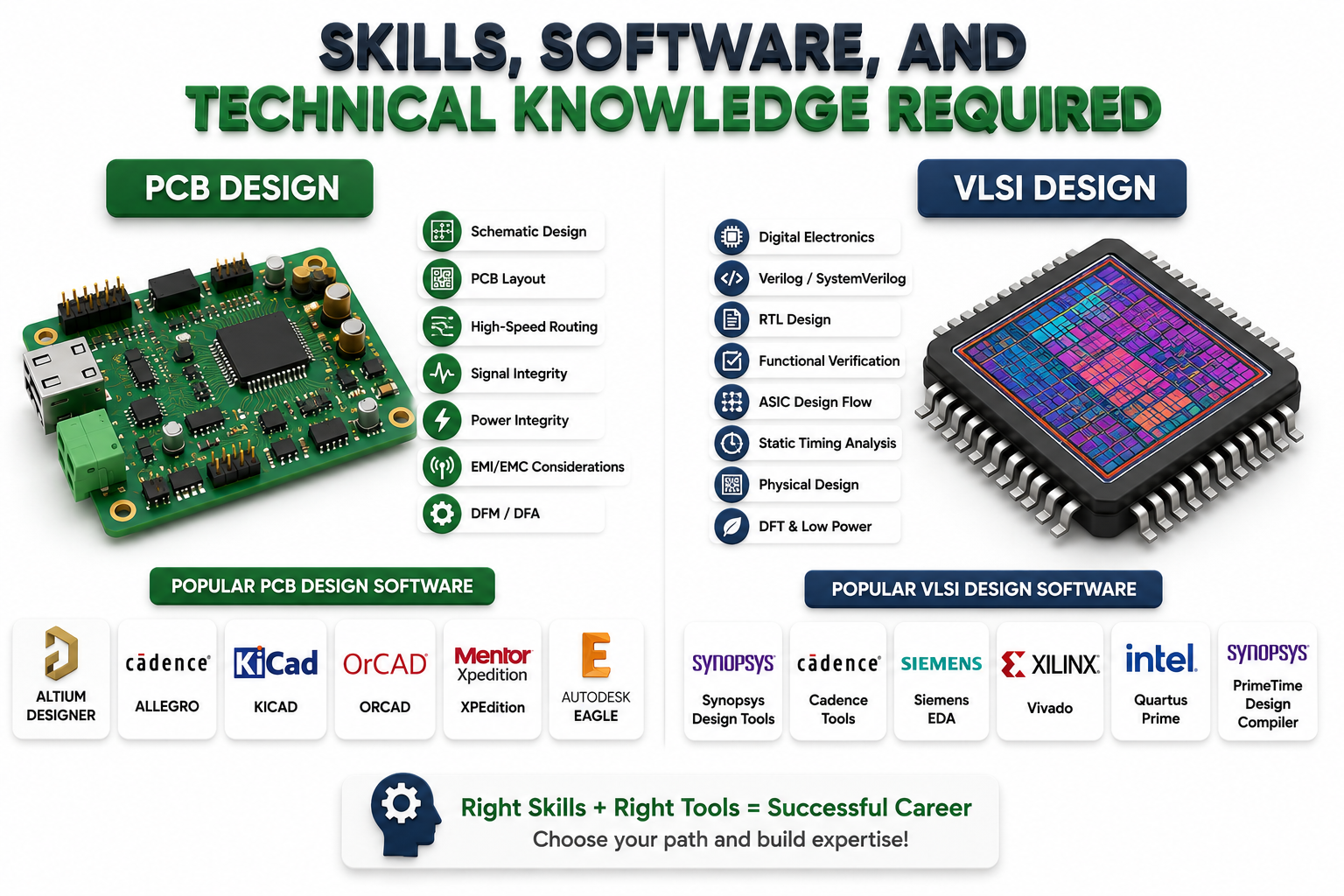
Success in either career depends on developing the right technical skills and becoming proficient with industry-standard tools.
PCB Design professionals typically work with:
Schematic design
PCB layout
High-speed routing
Signal integrity
Power integrity
EMI/EMC considerations
Design for Manufacturing (DFM)
Design for Assembly (DFA)
Popular PCB tools include Altium Designer, Cadence Allegro, KiCad, OrCAD, Mentor Xpedition, and Autodesk Eagle.
VLSI Design engineers focus on:
Digital electronics
Verilog and SystemVerilog
RTL Design
Functional Verification
ASIC Design Flow
Static Timing Analysis
Physical Design
Design for Testability (DFT)
Low-power design concepts
Industry-standard VLSI tools include Synopsys, Cadence, Siemens EDA, Vivado, Quartus, PrimeTime, Design Compiler, and Innovus.
Because VLSI involves semiconductor design at the transistor and logic level, the learning curve is generally steeper than PCB Design. However, both fields reward engineers who build strong practical experience through real-world projects.
Career Opportunities, Industries, and Hiring Trends
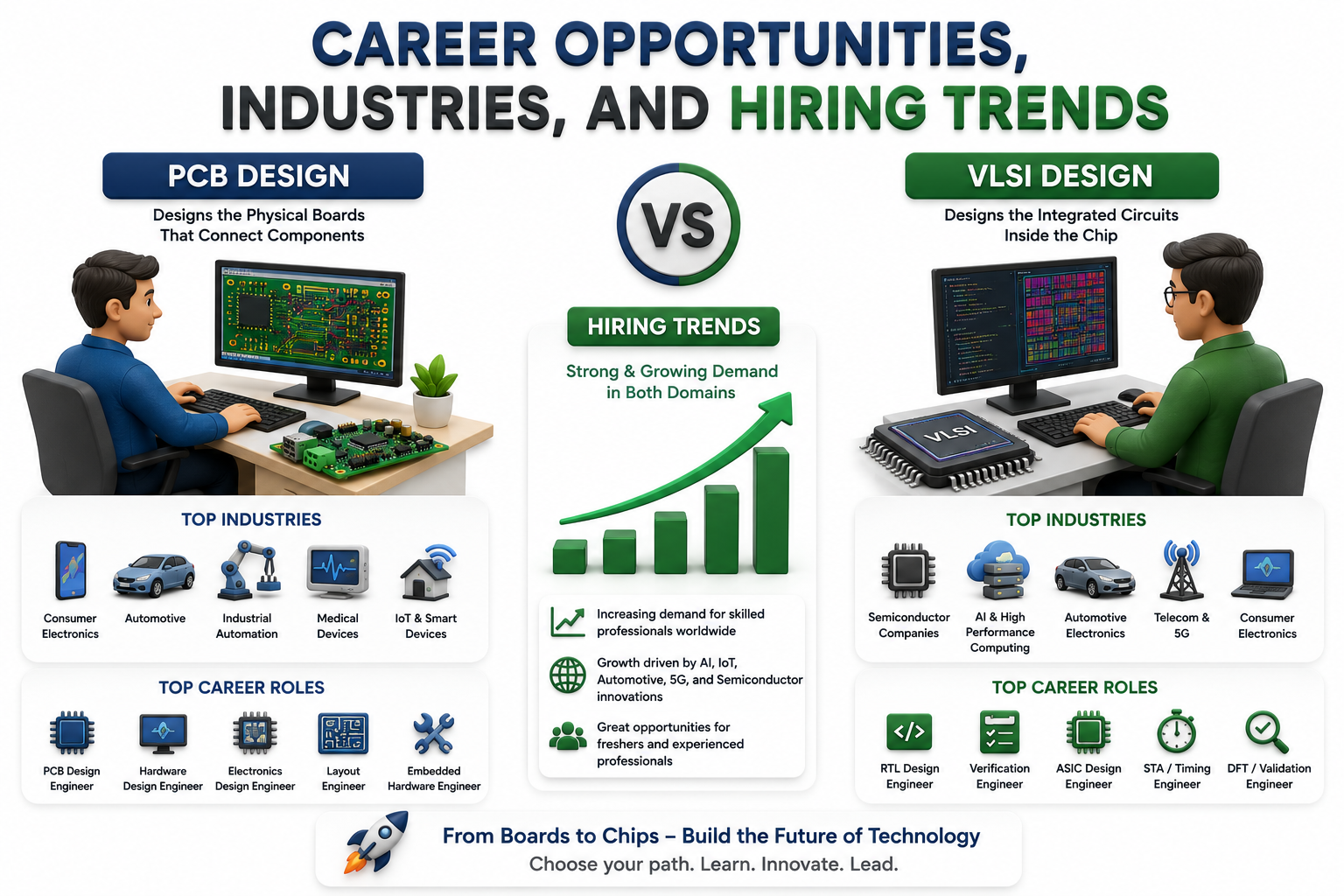
PCB Design offers opportunities across multiple industries because nearly every electronic product requires a printed circuit board. Companies developing embedded systems, robotics, industrial automation, electric vehicles, aerospace equipment, medical devices, and consumer electronics continuously hire skilled PCB designers.
VLSI Design careers are concentrated within the semiconductor ecosystem. Engineers are employed by semiconductor manufacturers, chip design companies, IP vendors, automotive semiconductor firms, AI hardware companies, networking organizations, and consumer electronics giants.
Typical PCB Design roles include:
PCB Design Engineer
Hardware Design Engineer
Electronics Design Engineer
Layout Engineer
Embedded Hardware Engineer
Common VLSI roles include:
RTL Design Engineer
Verification Engineer
Physical Design Engineer
DFT Engineer
STA Engineer
ASIC Design Engineer
FPGA Design Engineer
Post-Silicon Validation Engineer
As global investments in AI chips, automotive electronics, 5G infrastructure, and high-performance computing continue to grow, VLSI hiring has accelerated significantly. At the same time, PCB Design remains highly stable because every electronic product ultimately requires reliable hardware implementation.
Salary Comparison and Long-Term Career Growth
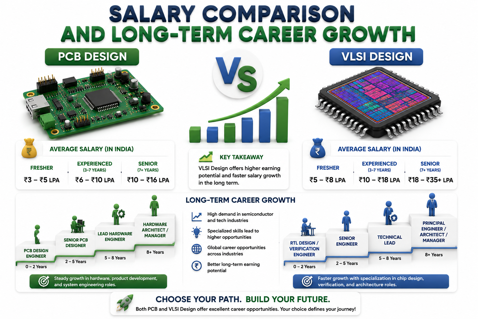
Salary is often one of the biggest deciding factors for engineering graduates. Although compensation varies depending on skills, company, and location, VLSI Design generally offers higher long-term earning potential because of its specialized expertise.
PCB Design professionals can steadily increase their salaries by gaining experience in high-speed design, RF layouts, multilayer boards, automotive electronics, and advanced manufacturing techniques.
VLSI engineers often experience faster salary growth as they specialize in areas such as:
ASIC Design
Functional Verification
Physical Design
Timing Closure
Low-Power Design
AI Accelerator Development
Career progression in both domains includes technical specialist, senior engineer, technical lead, engineering manager, and architect roles. However, VLSI careers often provide greater opportunities to work on cutting-edge semiconductor technologies used in artificial intelligence, data centers, smartphones, autonomous vehicles, and advanced computing systems.
Continuous learning remains essential because both industries evolve rapidly with new technologies, tools, and design methodologies.
Which Career Is Easier to Learn and Better for Freshers?
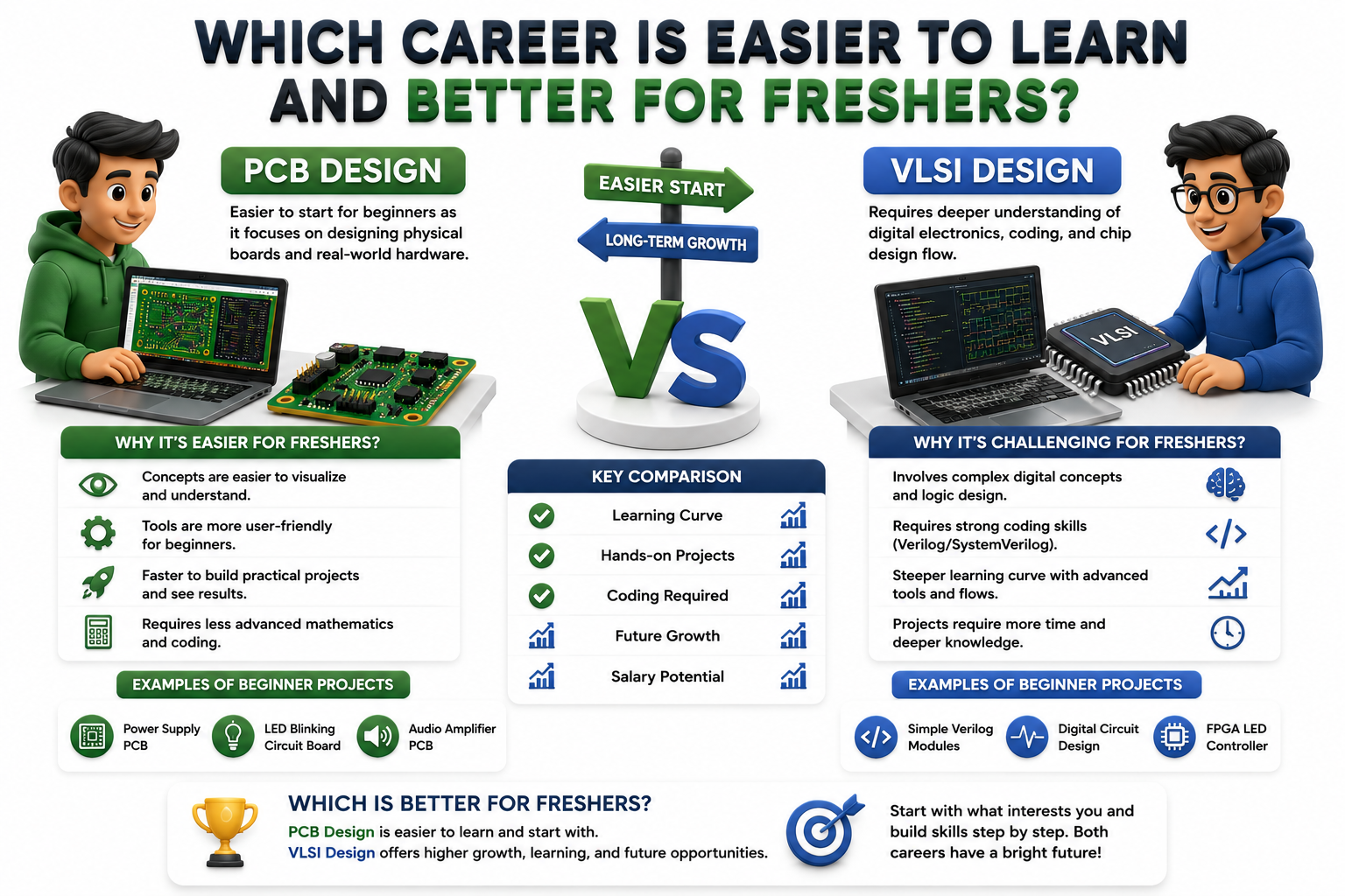
PCB Design is often considered more accessible for beginners because students can quickly understand schematic capture, component placement, routing, and board manufacturing concepts. Building practical PCB projects also requires comparatively fewer resources than semiconductor chip development.
VLSI Design demands stronger knowledge of:
Digital electronics
Computer architecture
Logic design
Semiconductor fundamentals
Hardware Description Languages (HDLs)
Timing concepts
Verification methodologies
Although VLSI has a steeper learning curve, structured practical training significantly improves employability. Working on RTL projects, verification environments, synthesis exercises, and FPGA implementations gives students valuable hands-on exposure that employers actively seek.
For aspiring VLSI professionals, practical industry-oriented training plays a major role. Programs offered by JastTech focus on real ASIC design flows, RTL Design, Functional Verification, Physical Design, and semiconductor projects that help students build job-ready skills aligned with current industry expectations.
Ultimately, neither career is inherently "better." The ideal choice depends on whether you enjoy designing complete hardware systems or developing the silicon chips that power modern electronic devices.
How to Choose the Right Career for Your Future
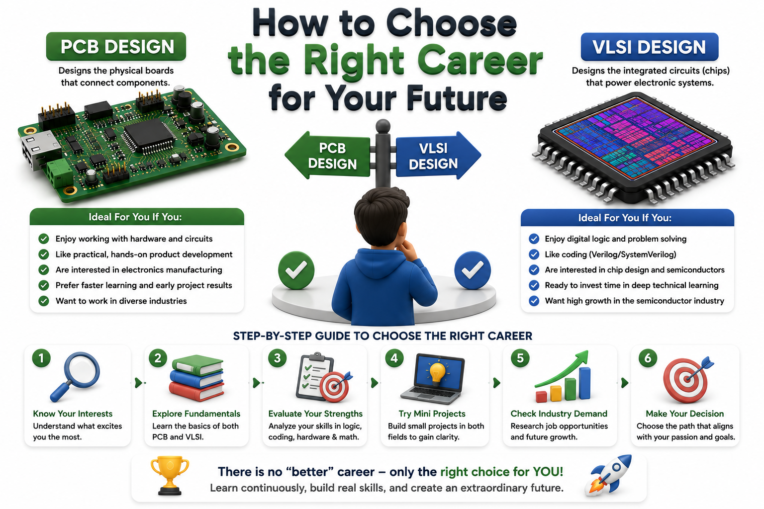
Selecting between PCB Design and VLSI Design should be based on your interests, strengths, and long-term career goals rather than salary alone.
PCB Design may be the right choice if you enjoy:
Hardware prototyping
Embedded systems
Product development
Circuit debugging
Manufacturing processes
Working with physical electronic products
VLSI Design may be a better fit if you enjoy:
Digital logic design
Semiconductor technology
Programming with Verilog/SystemVerilog
ASIC development
Chip verification
Solving complex design challenges
Students should also consider future industry trends. The rapid expansion of AI processors, automotive electronics, edge computing, high-speed networking, and semiconductor manufacturing is creating increasing demand for VLSI engineers worldwide. Meanwhile, the growth of IoT, industrial automation, robotics, renewable energy, and medical electronics continues to generate consistent demand for skilled PCB designers.
Before making a decision, explore beginner projects in both domains, learn the fundamental concepts, and evaluate which work excites you more. Practical experience often reveals your preferred specialization better than theoretical coursework alone.
Conclusion
PCB Design and VLSI Design are both rewarding career paths that contribute to the development of modern electronic products. PCB engineers transform circuit concepts into manufacturable hardware, while VLSI engineers design the integrated circuits that serve as the brains of those systems. Each discipline offers unique challenges, valuable technical skills, and excellent career opportunities for electronics graduates.
If your goal is to work in the rapidly growing semiconductor industry, investing in structured practical training can provide a significant advantage. Learning industry tools, building real-world projects, and understanding complete design workflows through platforms like JastTech can help bridge the gap between academic knowledge and industry expectations. Regardless of which path you choose, continuous learning and hands-on experience will remain the strongest foundations for a successful engineering career.