

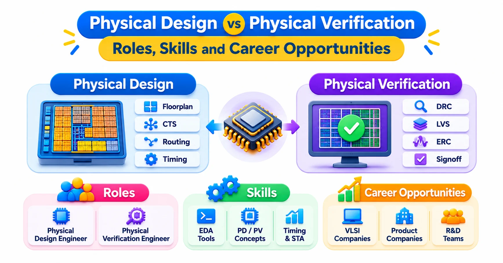
Physical Design vs Physical Verification: Roles, Skills and Career Opportunities
Navigate through this article using the table of contents below
Table of Contents
No headings found in this article.
A chip can have a flawless netlist, clean timing reports and a happy design team, and still be unmanufacturable. The gap between “it works on paper” and “the foundry will build it” is where two closely linked roles do their work. Understanding physical design vs physical verification helps you decide which one fits you, especially if you are planning a move into VLSI through a structured physical design training program.
Many freshers assume these are the same job with two names. They overlap in the same flow and the same tools, but the daily problems, the mindset and the career paths are different.
Two Jobs, One Layout: Where the Line Actually Sits
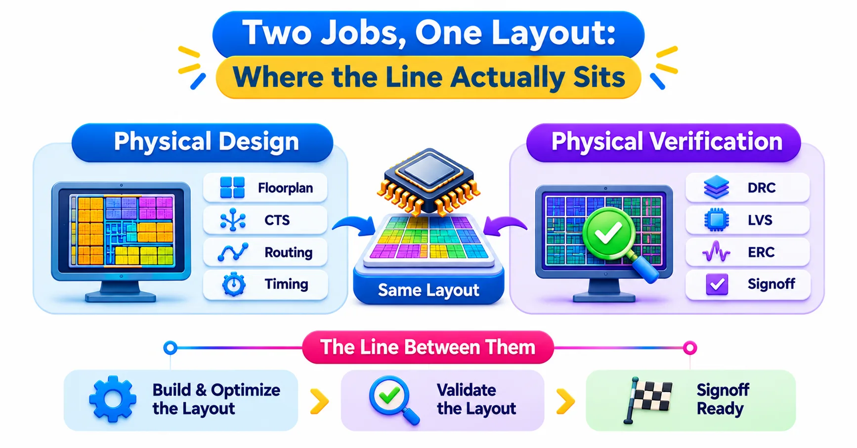
Physical design is the process of turning a logical circuit into a physical layout. Physical verification is the process of proving that the layout obeys the manufacturing rules and still matches the original circuit. One engineer builds the layout, and the other checks whether it can legally and correctly exist on silicon.
A useful comparison is construction versus inspection. Physical design engineers decide where blocks sit, how power reaches them, how clocks are distributed and how millions of wires are routed. Physical verification engineers take the finished or nearly finished layout and run it against the foundry’s rule deck. They ask three questions. Does it break any spacing or width rule? Does the layout still represent the schematic or netlist? Is anything likely to damage the chip during fabrication?
The line blurs because the two roles keep passing the design back and forth. A routing change by the design team can create hundreds of new rule violations. A verification finding can force the design team to reopen the floorplan. In a real project, this loop runs many times before tape-out.
In smaller companies, one engineer may do both. In larger semiconductor organizations and service companies, they are often separate roles, sometimes separate teams, with a handoff process between them. That distinction matters when you read job descriptions, because titles such as “Physical Design Engineer,” “PD Engineer” and “Physical Verification Engineer” can contain very different expectations.
What a Physical Design Engineer Does All Day
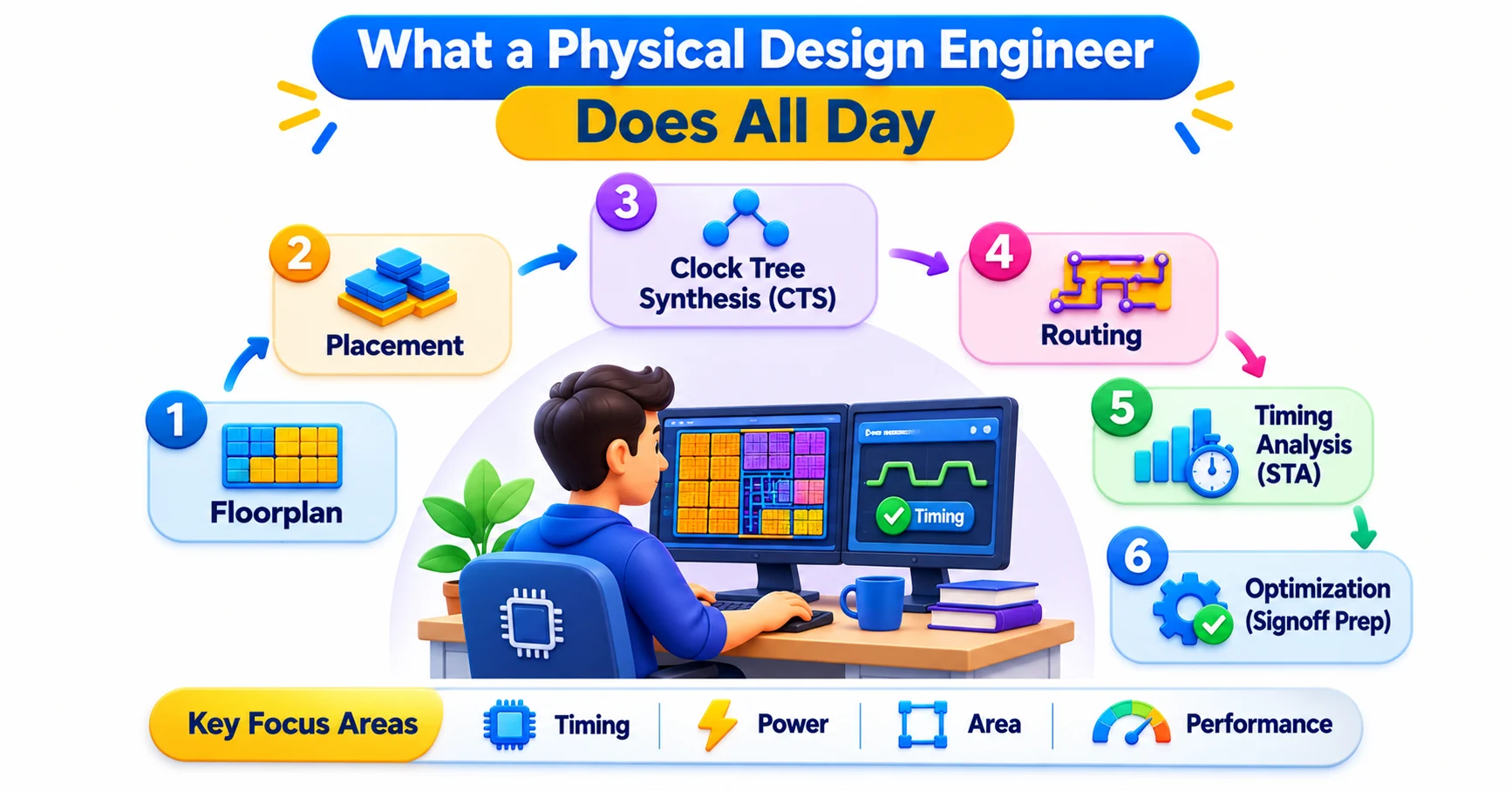
Physical design takes a synthesized netlist and produces a layout that meets timing, power and area targets. The work follows a fairly standard sequence, although every company adds its own flavor.
It usually starts with floorplanning, where the engineer decides the chip’s shape, places large macros such as memories, and plans the power grid. Placement follows, positioning millions of standard cells so that connected cells stay close without creating congestion. Clock tree synthesis then distributes the clock signal so that every flip-flop receives it at nearly the same time. Routing connects everything with metal layers, and the design goes through repeated optimization.
Timing is the thread that runs through all of this. Static timing analysis tells the engineer whether signals arrive early enough (setup) and stay stable long enough (hold). Much of a physical design engineer’s day is spent reading timing reports, understanding why a path fails and deciding whether to fix it by resizing cells, adding buffers, changing placement or applying an engineering change order. Power analysis, including IR drop and electromigration, adds another layer of checking.
A realistic example: a block misses setup timing on a few hundred paths after routing. The engineer notices that most of them pass through one congested area. The fix might involve adjusting macro placement, reducing local utilization, or reworking a clock skew decision, not simply swapping cells. The skill lies in diagnosing the root cause.
Commonly used tools in this space include Synopsys Fusion Compiler and IC Compiler II, and Cadence Innovus, with PrimeTime and Tempus used for signoff timing. Tool knowledge helps, but employers care more about whether you understand the reasoning behind each step.
What a Physical Verification Engineer Does All Day
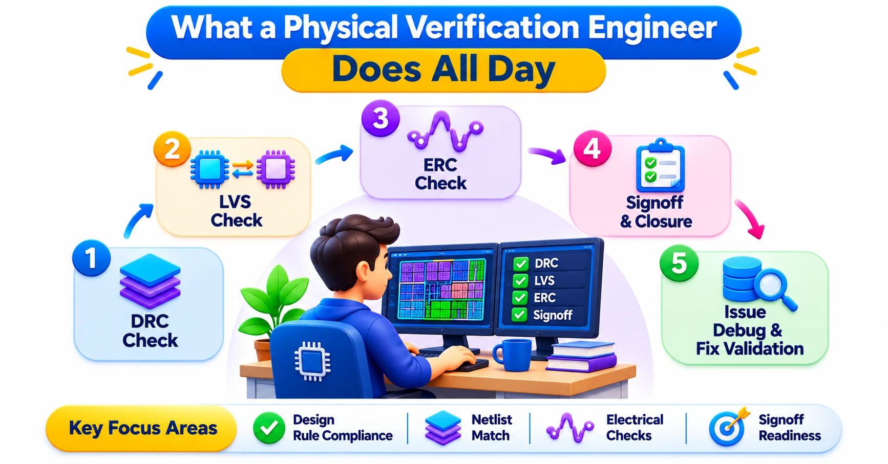
Physical verification is the discipline of signoff checking. The engineer runs the layout through rule decks supplied by the foundry and investigates every flagged result.
The core checks are well defined. Design rule checking (DRC) confirms that shapes obey minimum width, spacing, enclosure and density rules. Layout versus schematic (LVS) compares the extracted layout connectivity to the intended netlist, catching shorts, opens and mismatched devices. Electrical rule checking, antenna checks and checks for latch-up and ESD protection structures round out the picture. Modern processes also bring density and fill requirements, multi-patterning considerations and many more advanced rules.
The work is less about creating and more about interpreting. A DRC run on a full chip can produce thousands of violations, and a large share of them often trace back to one root cause, such as a bad cell placement, a missing via enclosure or an incorrectly handled macro boundary. A skilled verification engineer groups the errors, finds the pattern and sends a precise fix request instead of a raw error dump.
LVS debugging has its own flavor. A single missing connection or a floating net can cause a comparison to fail, and the engineer has to trace it back through hierarchy, labels and power connections. Patience and structured thinking matter more than speed here.
Siemens Calibre is the best-known signoff tool in this area, and Synopsys IC Validator and Cadence Pegasus are also widely used. Verification engineers frequently write or modify scripts, often in Tcl, Python or Perl, to automate result handling and to customize checks.
Skills Compared: Overlap, Differences and What Companies Test
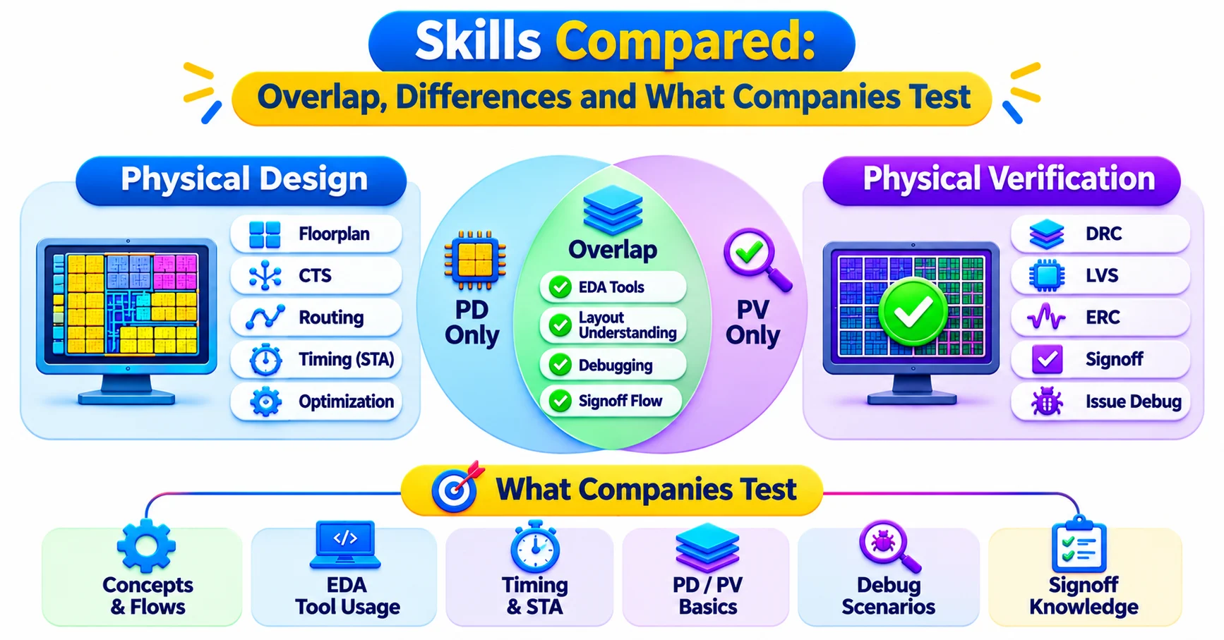
The two roles share a foundation. Both require a clear understanding of CMOS fundamentals, standard cell libraries, metal layers and the basics of the design flow. Both need comfort with Linux, scripting and reading large log files. Beginners who skip these basics struggle in either track.
The differences show up in emphasis. Physical design leans on timing concepts, clocking, power planning, congestion analysis and trade-offs between performance, power and area. Interviewers often ask about setup and hold fixing, clock skew and useful skew, floorplan decisions, utilization and how to reduce IR drop.
Physical verification leans on the foundry rule structure, layout geometry, device recognition and extraction, and debugging patterns. Interviewers ask what causes an LVS mismatch, how antenna violations are fixed, what density rules are for and how a hierarchical run differs from a flat run.
A simple way to judge your fit is to look at what you enjoy solving. If you like optimization puzzles with competing targets, physical design will feel natural. If you like methodical investigation, where the answer is either correct or flagged, physical verification may suit you better.
One misconception is worth correcting: physical verification is not an easier or lesser entry point. The rule decks of advanced nodes are complicated, and a missed violation can lead to a failed or low-yield chip, which is a very expensive mistake. Equally, physical design is not purely creative. Every decision is constrained by the same rules the verification team enforces.
Career Opportunities, Growth and the Hyderabad Angle

Both paths are open to electronics and electrical graduates, and in India the work is concentrated in cities with strong semiconductor design activity, including Bangalore, Hyderabad, Chennai and Pune. Product companies, EDA vendors, design service firms and foundry-linked teams all hire for these skills.
Physical design usually offers a broader ladder. An engineer often moves from block-level work to full-chip ownership, then to technical lead or physical design manager. Some move toward specialized areas such as low-power design, timing signoff or methodology and flow development. Physical verification offers a deeper specialist route. Engineers can grow into signoff leads, foundry interface roles, DFM specialists or EDA flow automation experts.
Movement between the two is common. A verification engineer who understands why violations appear is well positioned to learn design implementation, and a design engineer who has debugged signoff failures writes cleaner layouts. People who know both tend to be valued during tape-out crunch, when the two teams must work in lockstep.
For learners in Telangana, a local program such as physical design training in Hyderabad can make the practical side easier to access, since hands-on tool exposure is hard to get from theory alone. Salaries vary widely by company, node experience and city, so rely on current job listings and recruiter conversations rather than a single number from a blog.
Choosing Your Path and Building the Right Skills
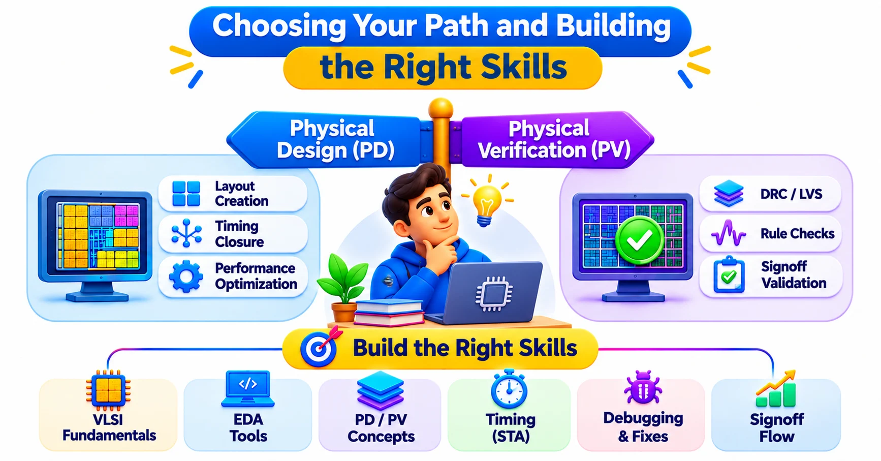
Start by learning the shared foundation: digital design basics, CMOS and layout concepts, STA fundamentals and the RTL-to-GDSII flow. This base lets you understand both sides before you commit.
Next, build practice rather than just notes. Work through a small block from floorplan to routing using any available tool environment, and learn to read timing, congestion and power reports. Then study the verification side by learning what each DRC and LVS error category means and why it occurs. Even if you choose design, this knowledge shortens your debugging time.
Pick up Tcl and Python early. Almost every real flow uses scripting, and engineers who automate repetitive checks stand out quickly.
Common beginner mistakes include memorizing command names without understanding the flow, ignoring STA until late, and treating verification as a final button press rather than a continuous process. A better habit is to explain every step aloud: what goes in, what comes out and what can go wrong.
Training environments such as JastTech’s can help structure that practice, but the deciding factor is always how much real debugging you do yourself. Run the flow, break it, and learn why it broke.
Conclusion
Physical design builds the layout, and physical verification proves it can be manufactured and that it matches the intended circuit. Knowing the difference between physical design vs physical verification lets you choose a path based on how you like to work, and the skills you gain in one will strengthen the other. In silicon, the person who creates and the person who checks both decide whether the chip ships.