

Post Silicon Validation vs Design Verification: Which Career Path is Better?
Navigate through this article using the table of contents below
Table of Contents
No headings found in this article.
Imagine being part of the team that ensures a chip works flawlessly before it is manufactured—or being the engineer who validates the actual silicon after it comes out of the fab. Both Post Silicon Validation and Design Verification are critical domains in the VLSI industry, offering exciting career opportunities for aspiring semiconductor engineers. As the demand for advanced chips continues to grow in industries such as AI, automotive electronics, IoT, and high-performance computing, professionals with expertise in these fields are becoming increasingly valuable.
When comparing Post Silicon Validation vs Design Verification, many students and professionals wonder which career path offers better growth, higher salaries, stronger job opportunities, and long-term stability. While Design Verification focuses on identifying and fixing design bugs during the pre-silicon stage using simulation and verification methodologies, Post Silicon Validation involves testing and debugging real hardware after chip fabrication. Understanding the differences, required skills, career prospects, and industry demand for both domains can help you make an informed decision about which VLSI career path is better suited to your interests and goals.
What is Post Silicon Validation?

Post Silicon Validation is a crucial stage in the semiconductor development lifecycle that takes place after a chip has been fabricated and manufactured. The primary goal of post-silicon validation is to verify that the physical silicon behaves exactly as intended according to the design specifications. Engineers perform extensive testing, debugging, performance analysis, and functionality checks on the actual hardware to identify any issues that may not have been detected during simulation and pre-silicon verification stages. This process helps ensure that the chip meets quality, reliability, power, and performance requirements before it is released for commercial use.
Post Silicon Validation engineers work with development boards, oscilloscopes, logic analyzers, protocol analyzers, and specialized validation tools to test real-world chip behavior. They validate interfaces such as PCIe, USB, Ethernet, DDR, and other communication protocols while analyzing system-level interactions and hardware performance. As semiconductor technologies become more complex with applications in artificial intelligence, automotive electronics, IoT, and data centers, the demand for skilled Post Silicon Validation professionals continues to grow. Their expertise plays a vital role in delivering stable, high-performance semiconductor products to the market while minimizing costly design flaws and product failures.
What is Design Verification?
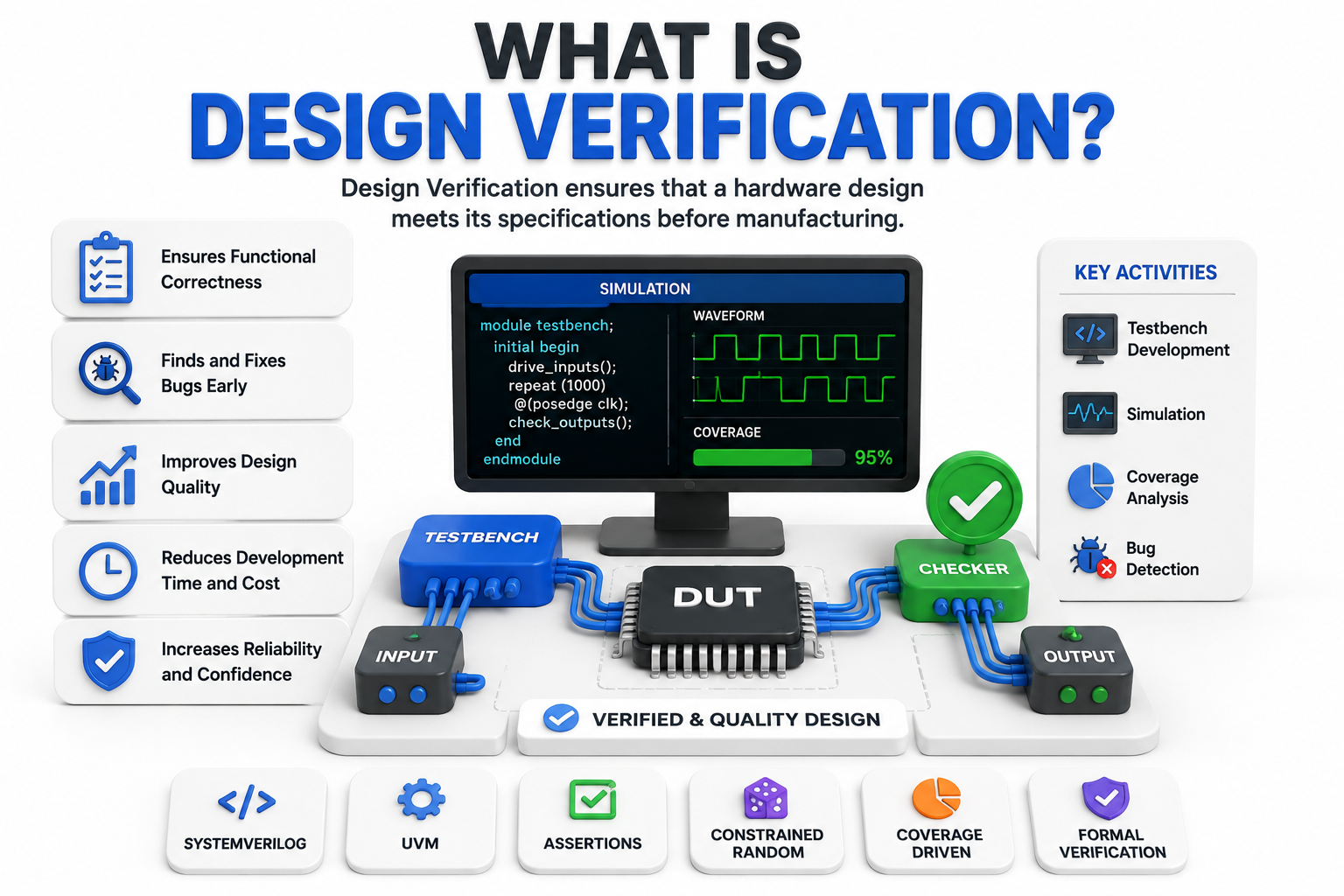
Design Verification is a critical phase in the semiconductor design process that ensures a chip design functions correctly before it is sent for fabrication. It is performed during the pre-silicon stage, where engineers verify that the Register Transfer Level (RTL) design meets all functional requirements and design specifications. The main objective of design verification is to identify and eliminate bugs, logic errors, and functional issues through simulation, emulation, and formal verification techniques. Since manufacturing a chip is extremely expensive, finding and fixing defects before fabrication helps reduce development costs and prevents costly redesigns.
Design Verification engineers use advanced methodologies such as SystemVerilog, Universal Verification Methodology (UVM), assertion-based verification, and coverage-driven verification to create comprehensive test environments. They develop testbenches, generate test cases, analyze simulation results, and ensure that every feature of the design is thoroughly validated under different operating conditions. With the rapid growth of technologies such as artificial intelligence, 5G, automotive electronics, IoT, and high-performance computing, Design Verification has become one of the most in-demand domains in the VLSI industry. Strong verification practices help semiconductor companies deliver reliable, high-quality chips while accelerating time-to-market and improving overall product success.
Post Silicon Validation vs Design Verification: Key Differences
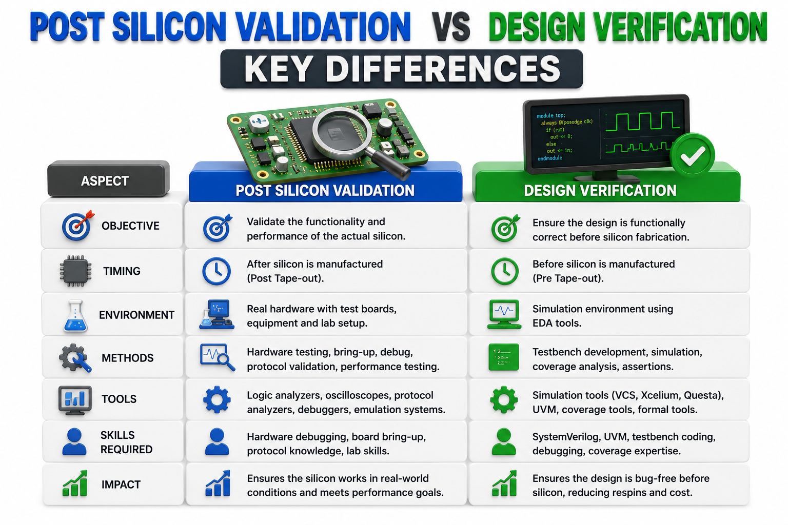
Post Silicon Validation
Post Silicon Validation is performed after a semiconductor chip has been fabricated and manufactured. The primary objective is to verify that the actual silicon operates according to the original design specifications under real-world conditions. Engineers test physical hardware using validation platforms, development boards, and laboratory equipment to identify performance issues, functional bugs, power-related problems, and protocol compliance errors that may not have been detected during earlier stages of development. This phase is critical because it confirms the reliability and stability of the chip before mass production and commercial deployment.
Post Silicon Validation engineers focus heavily on hardware debugging, system-level testing, performance optimization, and root-cause analysis. Their work involves validating interfaces such as PCIe, USB, Ethernet, DDR, and other high-speed communication protocols on real silicon. Since they work directly with fabricated chips, they gain extensive exposure to hardware behavior, signal integrity, and system interactions. This role is ideal for professionals who enjoy hands-on lab work, hardware troubleshooting, and solving complex issues in physical semiconductor devices.
Design Verification
Design Verification takes place before chip fabrication and focuses on ensuring that the RTL design behaves correctly according to functional specifications. The main goal is to identify and fix design bugs during the pre-silicon stage using simulation, emulation, formal verification, and advanced verification methodologies. By detecting issues before manufacturing, Design Verification helps semiconductor companies reduce development costs, avoid expensive silicon re-spins, and accelerate product development cycles.
Design Verification engineers primarily work with SystemVerilog, UVM, assertions, coverage metrics, and simulation tools to create verification environments and testbenches. Their responsibilities include writing test cases, analyzing simulation results, tracking functional coverage, and validating design functionality under numerous scenarios. Unlike Post Silicon Validation, which focuses on physical hardware testing, Design Verification is centered around virtual models and simulation-based verification. This career path is well-suited for professionals who enjoy coding, automation, verification methodologies, and ensuring design correctness before the chip reaches the manufacturing stage.
Skills Required for Post Silicon Validation Engineers

Post Silicon Validation Engineers require a strong combination of hardware knowledge, debugging expertise, and analytical problem-solving skills to ensure that fabricated chips function correctly in real-world environments. A solid understanding of digital electronics, computer architecture, ASIC and SoC design, communication protocols, and semiconductor fundamentals is essential. Engineers must be capable of performing hardware bring-up, executing validation test plans, analyzing system behavior, and identifying issues related to performance, power consumption, and functionality. Knowledge of interfaces such as PCIe, USB, Ethernet, DDR, I2C, SPI, and UART is highly valuable, as these protocols are commonly tested during silicon validation.
In addition to hardware expertise, Post Silicon Validation Engineers should possess proficiency in scripting and automation using languages such as Python, Shell scripting, or Perl to streamline testing and data analysis. Familiarity with laboratory instruments including oscilloscopes, logic analyzers, protocol analyzers, and signal generators is also important for effective debugging and troubleshooting. Strong communication and documentation skills help engineers collaborate with design, verification, firmware, and software teams to resolve complex issues efficiently. As modern semiconductor devices become increasingly sophisticated, professionals who combine technical knowledge with practical debugging experience are highly sought after in the VLSI and semiconductor industry.
Skills Required for Design Verification Engineers
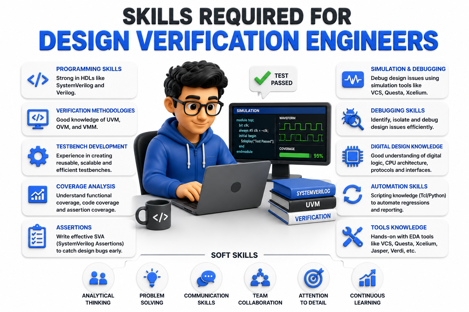
Design Verification Engineers require a strong foundation in digital electronics, computer architecture, RTL design concepts, and semiconductor fundamentals to effectively verify complex chip designs. One of the most important skills is proficiency in Hardware Description and Verification Languages such as Verilog, SystemVerilog, and VHDL. Engineers must understand verification methodologies, testbench architecture, simulation concepts, and functional coverage techniques to ensure that every aspect of a design operates according to specifications. Knowledge of ASIC and SoC design flows, finite state machines, memory architectures, and industry-standard communication protocols further enhances an engineer’s ability to identify and resolve design issues during the pre-silicon stage.
In addition to technical expertise, Design Verification Engineers should be skilled in using advanced verification methodologies such as Universal Verification Methodology (UVM), assertion-based verification, constrained-random verification, and formal verification techniques. Familiarity with EDA tools from leading vendors and scripting languages such as Python, Perl, Tcl, or Shell scripting is valuable for automating verification tasks and improving productivity. Strong analytical thinking, debugging abilities, and problem-solving skills are essential for identifying functional bugs and achieving coverage goals. As semiconductor designs continue to grow in complexity, professionals with expertise in SystemVerilog, UVM, verification planning, and coverage-driven verification remain highly sought after across the global VLSI industry.
Salary Comparison: Post Silicon Validation vs Design Verification
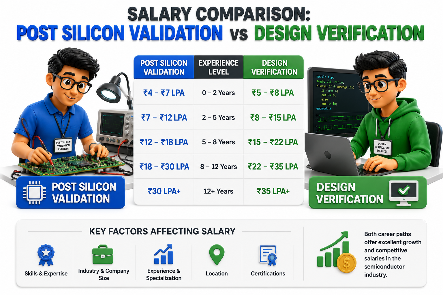
Salary is one of the most important factors professionals consider when choosing between Post Silicon Validation and Design Verification careers. Both domains offer competitive compensation packages due to the growing demand for skilled VLSI engineers in the semiconductor industry. For freshers in India, Post Silicon Validation Engineers typically earn between ₹4 LPA and ₹8 LPA, while Design Verification Engineers often start with salaries ranging from ₹5 LPA to ₹10 LPA, depending on their technical expertise, academic background, project experience, and the company they join. Professionals with hands-on experience in advanced verification methodologies or hardware debugging generally command higher starting packages.
At the mid-career level, both career paths provide significant salary growth opportunities. Post Silicon Validation Engineers with expertise in protocol validation, silicon bring-up, performance analysis, and system-level debugging can earn between ₹10 LPA and ₹25 LPA. Similarly, Design Verification Engineers skilled in SystemVerilog, UVM, assertion-based verification, and coverage-driven verification often earn salaries ranging from ₹12 LPA to ₹30 LPA. Since Design Verification requires specialized verification methodologies and extensive coding skills, it frequently offers slightly higher compensation in many semiconductor organizations.
For senior professionals and technical leaders, salary differences become more dependent on expertise, project impact, and leadership responsibilities rather than the specific domain itself. Experienced Post Silicon Validation Managers, Principal Engineers, and Architects can earn ₹30 LPA to ₹60 LPA or more, while senior Design Verification experts, Verification Leads, and Verification Architects may earn ₹35 LPA to ₹70 LPA or higher in top semiconductor companies. Ultimately, both career paths offer excellent earning potential, long-term job security, and strong growth prospects, making them attractive options for engineers seeking successful careers in the VLSI and semiconductor industry.
Job Opportunities and Industry Demand in 2026

The demand for Post Silicon Validation and Design Verification professionals continues to grow rapidly in 2026 as the global semiconductor industry expands to support technologies such as artificial intelligence, 5G networks, autonomous vehicles, IoT devices, cloud computing, and high-performance processors. Semiconductor companies are investing heavily in the development of advanced ASICs, SoCs, and custom silicon solutions, creating a strong need for engineers who can ensure chip functionality and reliability. As chip complexity increases, organizations are actively hiring skilled validation and verification engineers to reduce design risks, improve product quality, and accelerate time-to-market.
Design Verification remains one of the largest employment segments within the VLSI industry due to the significant effort required to verify modern chip designs before fabrication. Engineers with expertise in SystemVerilog, UVM, formal verification, and coverage-driven verification are highly sought after by semiconductor companies, design service firms, and EDA tool providers. At the same time, Post Silicon Validation professionals are experiencing increased demand as advanced semiconductor products require extensive hardware testing, protocol validation, performance analysis, and silicon debugging before commercial deployment. Engineers with hands-on laboratory experience and strong debugging skills are particularly valued in this domain.
Leading semiconductor companies such as Intel Corporation, AMD, NVIDIA, Qualcomm, Broadcom, Texas Instruments, MediaTek, and Samsung Electronics continue to recruit engineers for both verification and validation roles. With semiconductor innovation accelerating worldwide and India emerging as a major chip design hub, professionals in Post Silicon Validation and Design Verification can expect strong job opportunities, competitive salaries, and excellent long-term career growth throughout 2026 and beyond.
Challenges in Post Silicon Validation and Design Verification
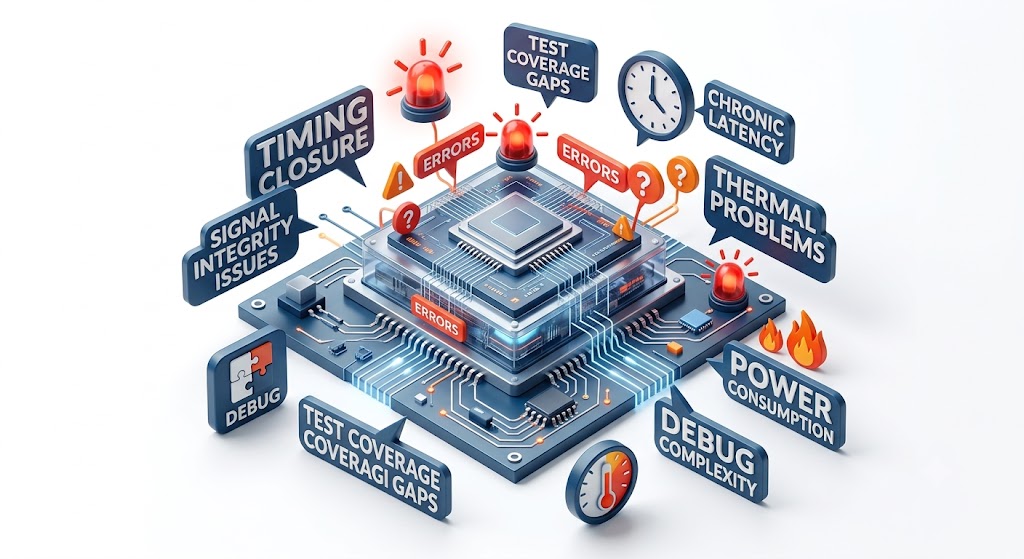
Post Silicon Validation and Design Verification are both technically demanding domains that require engineers to solve complex problems under strict project timelines. In Post Silicon Validation, one of the biggest challenges is debugging issues on actual silicon, where failures may result from hardware, firmware, software, or system-level interactions. Identifying the root cause of a problem can be time-consuming because engineers must analyze real-world behavior using laboratory equipment, protocol analyzers, and performance monitoring tools. Additionally, limited visibility into internal chip signals compared to simulation environments makes debugging more difficult, requiring strong analytical skills and extensive hardware knowledge.
Design Verification presents its own set of challenges due to the increasing complexity of modern ASIC and SoC designs. Verification engineers must create comprehensive test environments capable of validating millions of design scenarios while ensuring maximum functional coverage. Developing robust UVM-based testbenches, debugging simulation failures, managing coverage closure, and verifying multiple design blocks within tight development schedules can be demanding. As advanced technologies such as AI accelerators, 5G chipsets, and automotive processors continue to evolve, verification complexity grows significantly, requiring engineers to continuously update their skills, learn new methodologies, and adapt to rapidly changing semiconductor design requirements.
Post Silicon Validation vs Design Verification: Future Scope
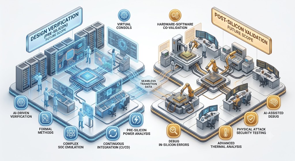
The future scope of both Post Silicon Validation and Design Verification is exceptionally strong as the semiconductor industry continues to advance with technologies such as artificial intelligence, machine learning, 5G communication, autonomous vehicles, edge computing, and the Internet of Things (IoT). Modern chips are becoming more complex, integrating billions of transistors and multiple functional blocks into a single System-on-Chip (SoC). As a result, semiconductor companies require highly skilled engineers to verify design correctness before fabrication and validate silicon performance after manufacturing. This growing complexity ensures long-term demand for professionals in both domains across global technology markets.
Design Verification is expected to remain one of the most critical and fastest-growing areas in VLSI because verification activities often consume a significant portion of the overall chip development cycle. Companies are increasingly investing in advanced verification methodologies, automation, formal verification, AI-assisted verification tools, and coverage-driven verification techniques to reduce design risks and accelerate product launches. Engineers with expertise in SystemVerilog, UVM, assertions, and verification automation will continue to enjoy strong career opportunities, competitive salaries, and access to cutting-edge semiconductor projects.
Post Silicon Validation is also gaining importance as advanced processors, AI accelerators, networking devices, automotive chips, and high-performance computing systems require extensive real-world testing before deployment. The need for silicon bring-up, protocol validation, performance tuning, power analysis, and system-level debugging is increasing with every new generation of semiconductor products. As industries demand higher reliability and performance from electronic devices, Post Silicon Validation engineers will play a vital role in ensuring product quality and market readiness. In the coming years, both career paths are expected to offer excellent job security, global opportunities, and strong professional growth, making them highly attractive options for aspiring VLSI engineers.
Conclusion: Post Silicon Validation vs Design Verification – Which Career Path Should You Choose?
Choosing between Post Silicon Validation and Design Verification ultimately depends on your interests, technical strengths, and long-term career goals. If you enjoy working with actual hardware, laboratory equipment, protocol testing, silicon bring-up, and system-level debugging, Post Silicon Validation can be a highly rewarding career path. On the other hand, if you prefer coding, simulation, testbench development, SystemVerilog, UVM, and identifying design issues before chip fabrication, Design Verification may be a better fit. Both domains play a crucial role in the semiconductor development lifecycle and offer opportunities to work on cutting-edge technologies such as AI processors, 5G chipsets, automotive electronics, and high-performance computing systems.
From a career perspective, both Post Silicon Validation and Design Verification provide strong job demand, attractive salaries, and excellent growth opportunities in the VLSI industry. Design Verification often offers a larger number of job openings due to the extensive verification effort required in modern chip development, while Post Silicon Validation provides valuable hands-on experience with real silicon and advanced hardware platforms. Rather than focusing solely on salary or popularity, aspiring engineers should choose the domain that aligns with their skills and interests. By building strong technical expertise and gaining practical project experience, professionals in either field can achieve long-term success and establish a rewarding career in the rapidly growing semiconductor industry.