

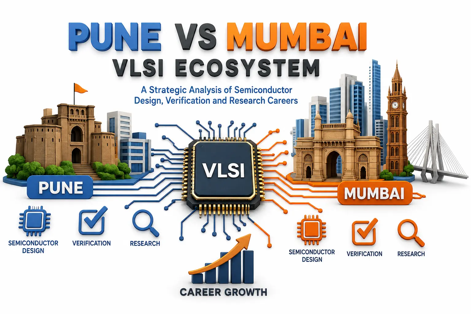
Pune vs Mumbai VLSI Ecosystem A Strategic Analysis of Semiconductor Design Verification and Research Careers
Navigate through this article using the table of contents below
Table of Contents
No headings found in this article.
Choosing between Pune and Mumbai for a VLSI career is no longer simply a question of which city has more technology companies. As semiconductor engineering expands in India, the real difference lies in the type of work, specialization, industry exposure and long-term opportunities each ecosystem can provide.
Pune is developing a visible concentration of semiconductor design and verification activity, while Mumbai brings together electronics, engineering services, research, startups and a much larger commercial ecosystem. For aspiring engineers, understanding these differences can influence everything from training choices to long-term specialization.
Pune and Mumbai Are Building Different VLSI Ecosystems
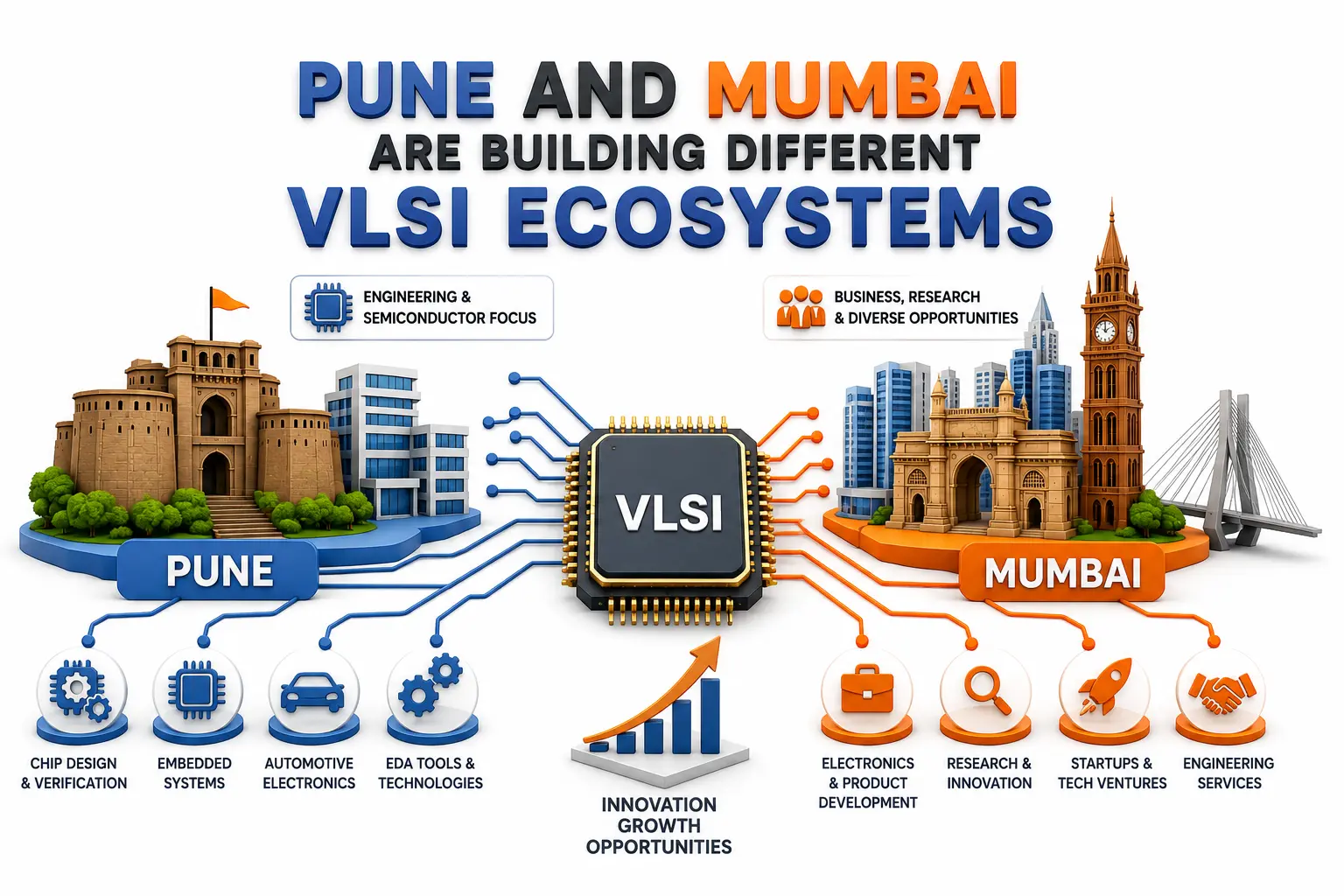
Pune's strength comes from its established engineering identity. The city combines automotive technology, embedded systems, software development, electronics engineering and semiconductor-related activities. This creates natural overlap between VLSI, embedded hardware, automotive electronics, SoC development and advanced engineering services.
Current hiring patterns also demonstrate opportunities around design verification, physical design, SoC verification and related semiconductor engineering. This makes Pune particularly relevant for engineers who want to work close to core chip-development workflows rather than treating VLSI as an isolated specialization.
Mumbai's semiconductor environment has a different character. Its enormous technology and business ecosystem creates opportunities across electronics companies, engineering services, startups, research institutions and specialized design organizations. The market may appear less concentrated around large semiconductor engineering centres than Pune, but it can still offer valuable paths for engineers interested in VLSI combined with broader electronics and technology domains.
The strategic difference can therefore be summarized as:
Pune: stronger concentration around engineering, embedded technology and semiconductor development.
Mumbai: broader technology ecosystem with VLSI opportunities distributed across different types of organizations.
Both cities: useful for building semiconductor careers when candidates develop specialization rather than relying on location alone.
Semiconductor Design Careers Give Pune a Strategic Advantage
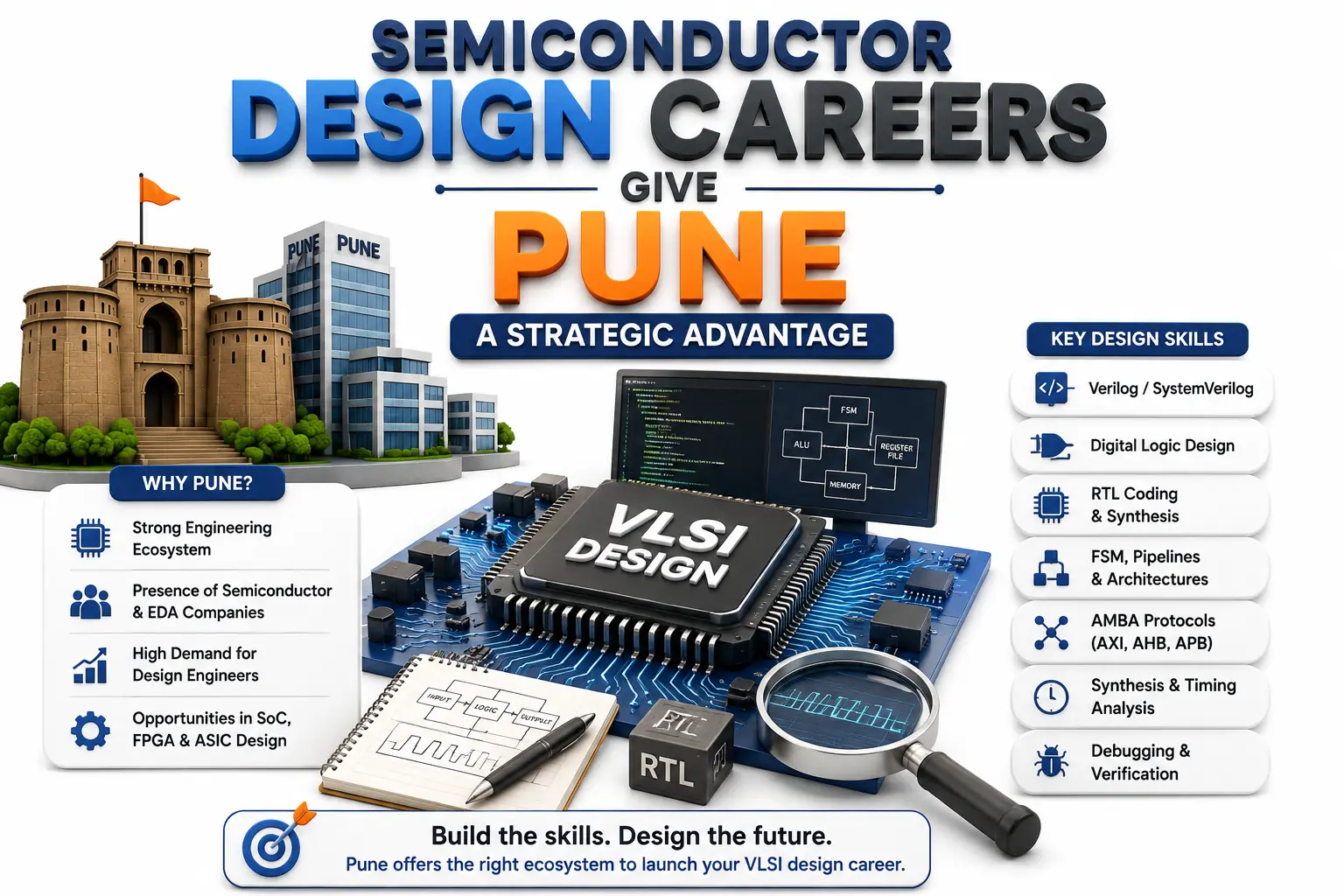
RTL design is one of the most technically demanding entry points into front-end VLSI. Engineers translate architectural requirements into synthesizable digital hardware using languages such as Verilog and SystemVerilog. Strong digital fundamentals, FSM design, timing concepts, computer architecture and debugging ability are essential.
Pune's engineering ecosystem makes it attractive for candidates targeting RTL, SoC, FPGA and digital-design-related careers. The presence of semiconductor, EDA, embedded and engineering organizations also gives professionals opportunities to move between connected domains as their careers develop.
Mumbai should not be excluded from a design-focused career strategy. Opportunities can emerge through specialized semiconductor companies, engineering service providers, FPGA development and electronics organizations. However, candidates should evaluate actual job descriptions instead of assuming every "VLSI" opening involves core RTL development.
For design careers, prioritize:
Digital electronics and computer architecture
Verilog and synthesizable SystemVerilog
RTL coding and linting
FSMs, memories and pipelining
Synthesis and static timing fundamentals
AMBA protocols such as AXI, AHB and APB
Linux and scripting skills
These capabilities make engineers more portable across cities because employers ultimately recruit for engineering competence rather than a postal address.
Design Verification Could Be Pune's Most Important Career Opportunity
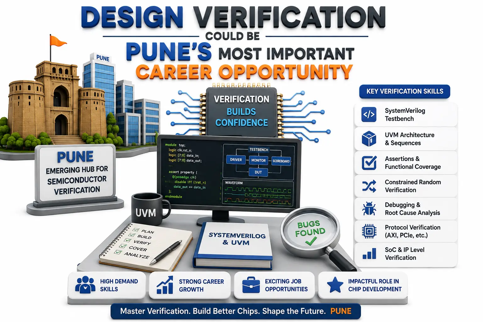
Verification is becoming increasingly important as SoCs integrate processors, interfaces, security functions, accelerators and complex IP blocks. A verification engineer must prove that the design behaves correctly across normal operations, corner cases and unexpected conditions before silicon reaches manufacturing.
Pune currently presents a particularly compelling environment for this path. Semiconductor roles in the market emphasize SystemVerilog, UVM, verification planning, testbench development, coverage, debugging, SoC-level verification and protocol knowledge. These requirements show why simply learning Verilog syntax is insufficient for serious verification careers.
Engineers targeting this field should build practical capability in:
SystemVerilog testbench development
UVM architecture and sequences
Assertions and functional coverage
Constrained-random verification
Debugging simulation failures
AXI, PCIe, Ethernet or other relevant protocols
Python, Perl, Shell or TCL scripting
IP and SoC-level verification concepts
Students searching for a vlsi training institute in pune should therefore evaluate the depth of projects, verification environments and EDA exposure rather than choosing solely on course duration or certification.
Mumbai Becomes More Interesting When Research and Specialization Matter
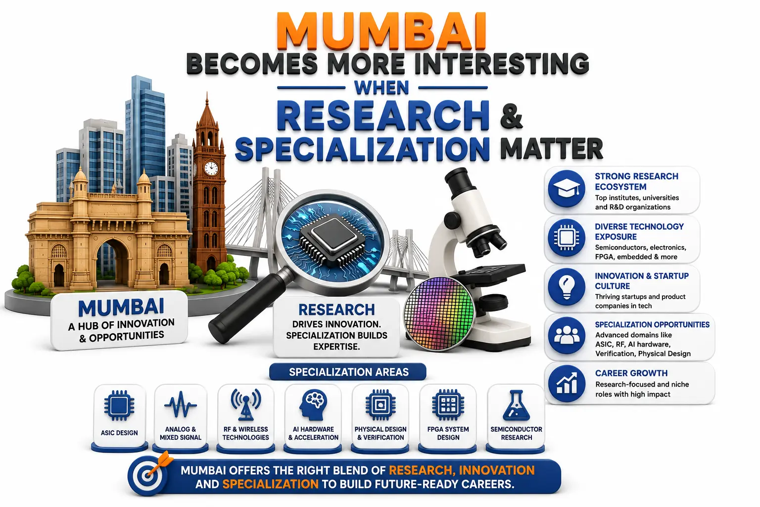
Mumbai's advantage becomes clearer when the definition of a semiconductor career expands beyond conventional RTL and verification jobs. Its academic, research, electronics and commercial networks can support engineers interested in semiconductor devices, specialized architectures, FPGA systems, electronic product development and research-oriented careers.
Research careers require a different preparation strategy. A verification engineer may focus heavily on UVM and coverage closure, whereas a research-oriented candidate may need deeper knowledge of CMOS devices, semiconductor physics, circuit design, computer architecture, algorithms or emerging hardware technologies.
This makes specialization important when evaluating a vlsi traininng institute in mumbai. Engineers should look beyond introductory HDL courses and determine whether the learning path supports the domain they actually want to enter.
JastTech, for example, focuses on industry-oriented VLSI skill development spanning areas such as RTL design, SystemVerilog, verification and practical semiconductor workflows. Regardless of the provider selected, candidates should prioritize hands-on implementation, debugging and project experience because these demonstrate engineering ability more effectively than certificates alone.
Skills Will Matter More Than the Pune-vs-Mumbai Debate
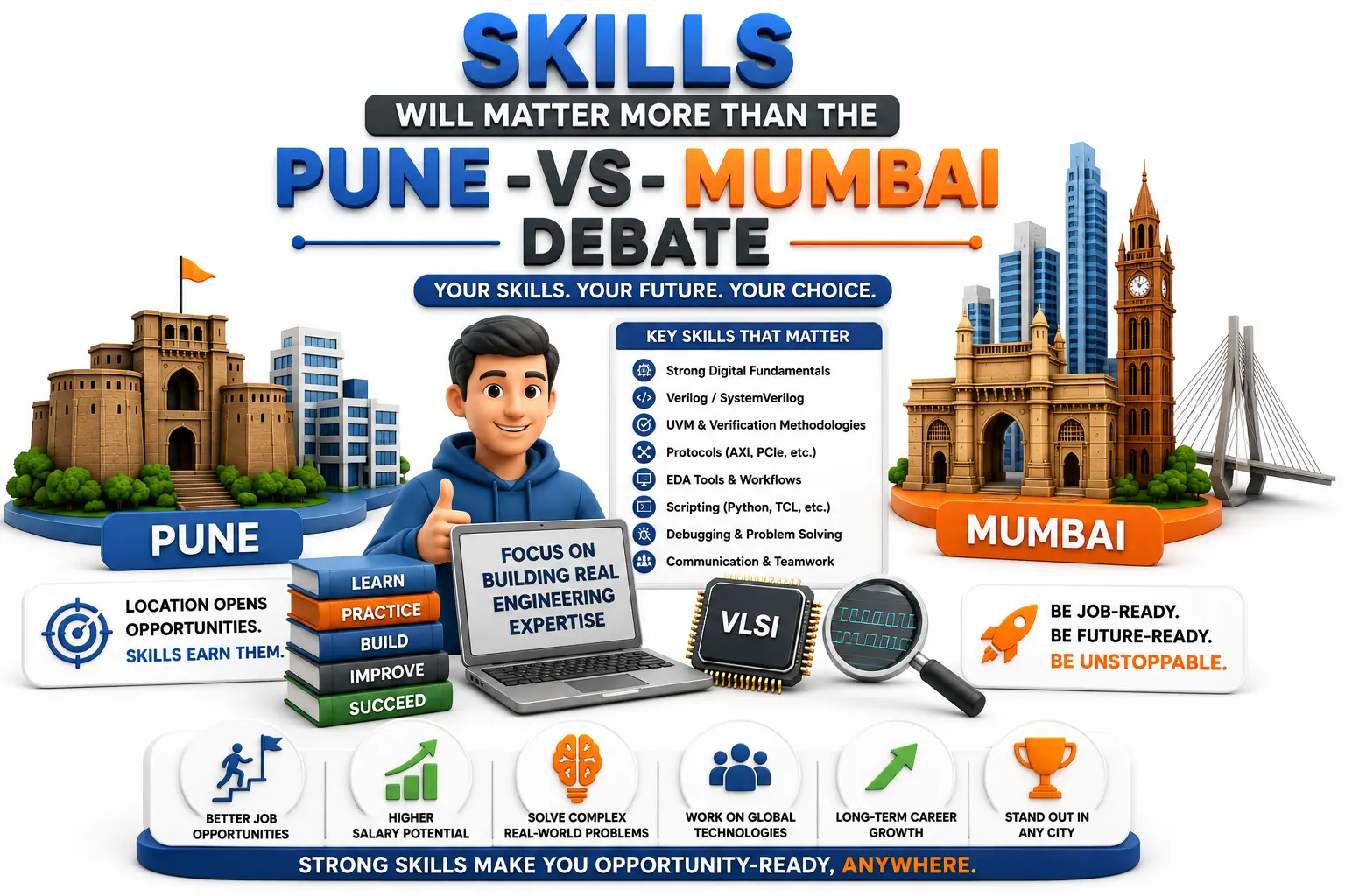
Location can create access to opportunities, but technical depth determines whether a candidate can convert those opportunities into a job. Modern semiconductor recruitment increasingly expects candidates to understand workflows rather than memorize definitions.
For an RTL role, build a project that demonstrates clean synthesizable coding, FSM implementation, timing awareness and verification. For a design-verification role, create a structured SystemVerilog/UVM environment containing sequences, drivers, monitors, scoreboards, assertions and functional coverage. Candidates interested in physical design should understand synthesis, floorplanning, placement, clock-tree synthesis, routing and timing closure.
A strong portfolio might include:
UART, SPI or I2C controller RTL
AXI-based design or verification project
UVM verification environment
FPGA implementation project
Synthesis and timing-analysis exercise
Python/TCL automation scripts
These projects create evidence of ability. An engineer in Mumbai with excellent verification skills can outperform an underprepared candidate in Pune despite Pune's stronger concentration of relevant employers.
Which City Should You Choose for Your VLSI Career?
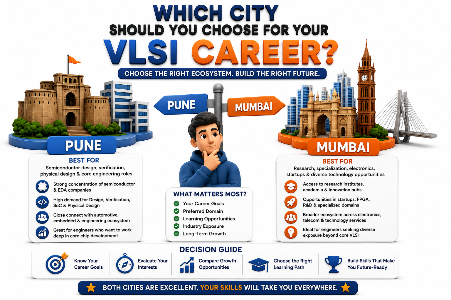
For engineers focused specifically on RTL design, SoC verification, physical design and semiconductor product development, Pune currently presents a particularly attractive environment. Its engineering ecosystem creates useful intersections between semiconductor design, automotive electronics, embedded systems and EDA-related work.
Mumbai remains valuable for candidates who want access to a wider commercial and research ecosystem or intend to combine VLSI with electronics, FPGA, R&D and related technology areas. Its scale also means career possibilities should be evaluated company by company rather than through the assumption that Mumbai must have the same semiconductor structure as Pune.
The best decision framework is straightforward:
Choose Pune when proximity to concentrated engineering and semiconductor activity is the priority.
Consider Mumbai when research, broader electronics exposure or multidisciplinary opportunities match your goals.
Prioritize verification skills if you enjoy debugging, testbench architecture and finding corner-case failures.
Prioritize RTL design if digital logic, microarchitecture and hardware implementation interest you.
Consider research if you enjoy deeper technical investigation and are prepared for postgraduate-level specialization.
Conclusion
Pune and Mumbai should not be treated as identical semiconductor markets. Pune's engineering-heavy environment currently gives it a strong position for VLSI design, SoC verification, physical design and connected embedded-system careers. Mumbai provides a broader ecosystem where semiconductor skills can intersect with research, electronics, FPGA development and technology services.
The more important career decision, however, is specialization. Engineers who master digital fundamentals, HDL coding, verification methodologies, protocols, EDA workflows and practical projects can compete across both cities and eventually across India's larger semiconductor market. Choose the ecosystem that supports your target role, but build skills strong enough that your career is never limited by geography.