

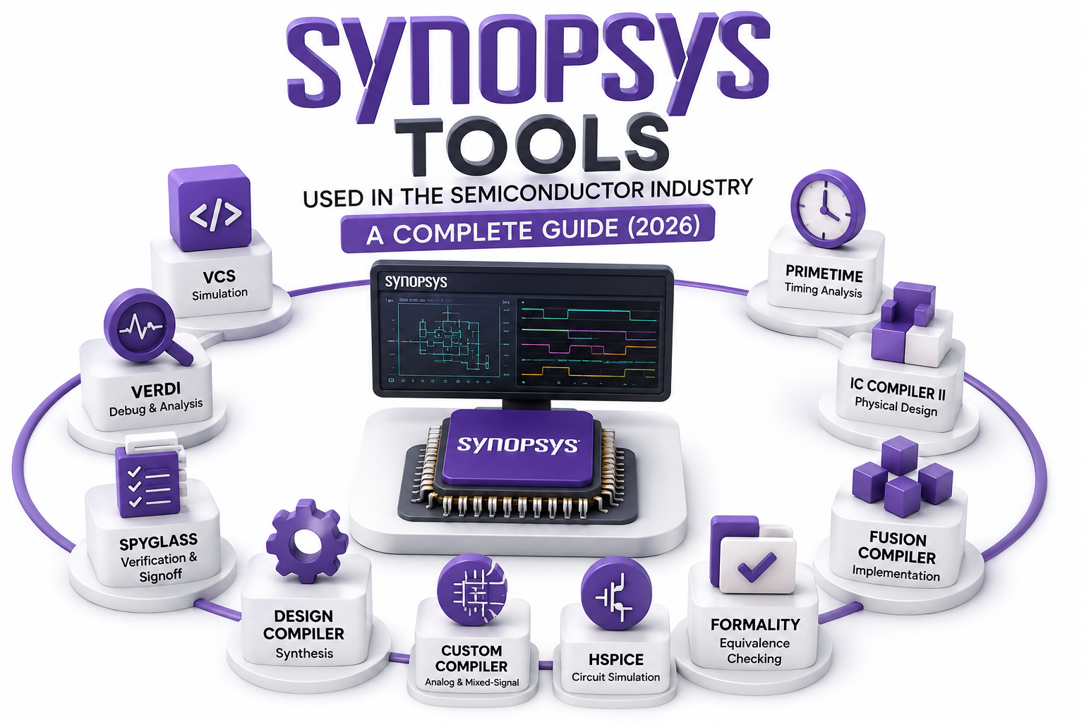
Synopsys Tools Used in the Semiconductor Industry: A Complete Guide (2026)
Navigate through this article using the table of contents below
Table of Contents
No headings found in this article.
Modern semiconductor chips contain billions of transistors, making manual design impossible. Behind every processor, AI accelerator, automotive SoC, or smartphone chip lies a sophisticated Electronic Design Automation (EDA) ecosystem. Among all EDA providers, Synopsys remains one of the industry's most influential technology leaders.
Whether you're an engineering student, an aspiring VLSI professional, or an experienced designer looking to understand today's semiconductor workflow, learning Synopsys tools has become a valuable career skill. This guide explains the major tools used across the complete chip development process and why mastering them through platforms like JastTech can help build industry-ready expertise.
Why Synopsys Tools Dominate Modern Semiconductor Design
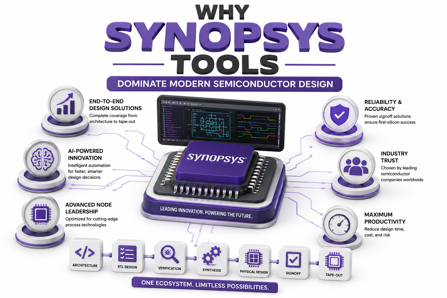
Designing an integrated circuit requires multiple engineering teams working across architecture, RTL development, verification, synthesis, physical implementation, timing analysis, and silicon validation. Synopsys provides specialized software for each stage, enabling companies to design increasingly complex chips with higher performance and lower power consumption.
The company's tools are trusted by leading semiconductor organizations because they support advanced manufacturing nodes, AI-driven optimization, and large-scale design automation. As chips continue to grow in complexity, Synopsys solutions help engineers improve productivity while reducing design risks.
Key advantages include:
End-to-end semiconductor design support
AI-assisted optimization capabilities
Compatibility with advanced process technologies
Strong verification and signoff ecosystem
Broad adoption across global semiconductor companies
Major Synopsys Tools and Their Primary Functions
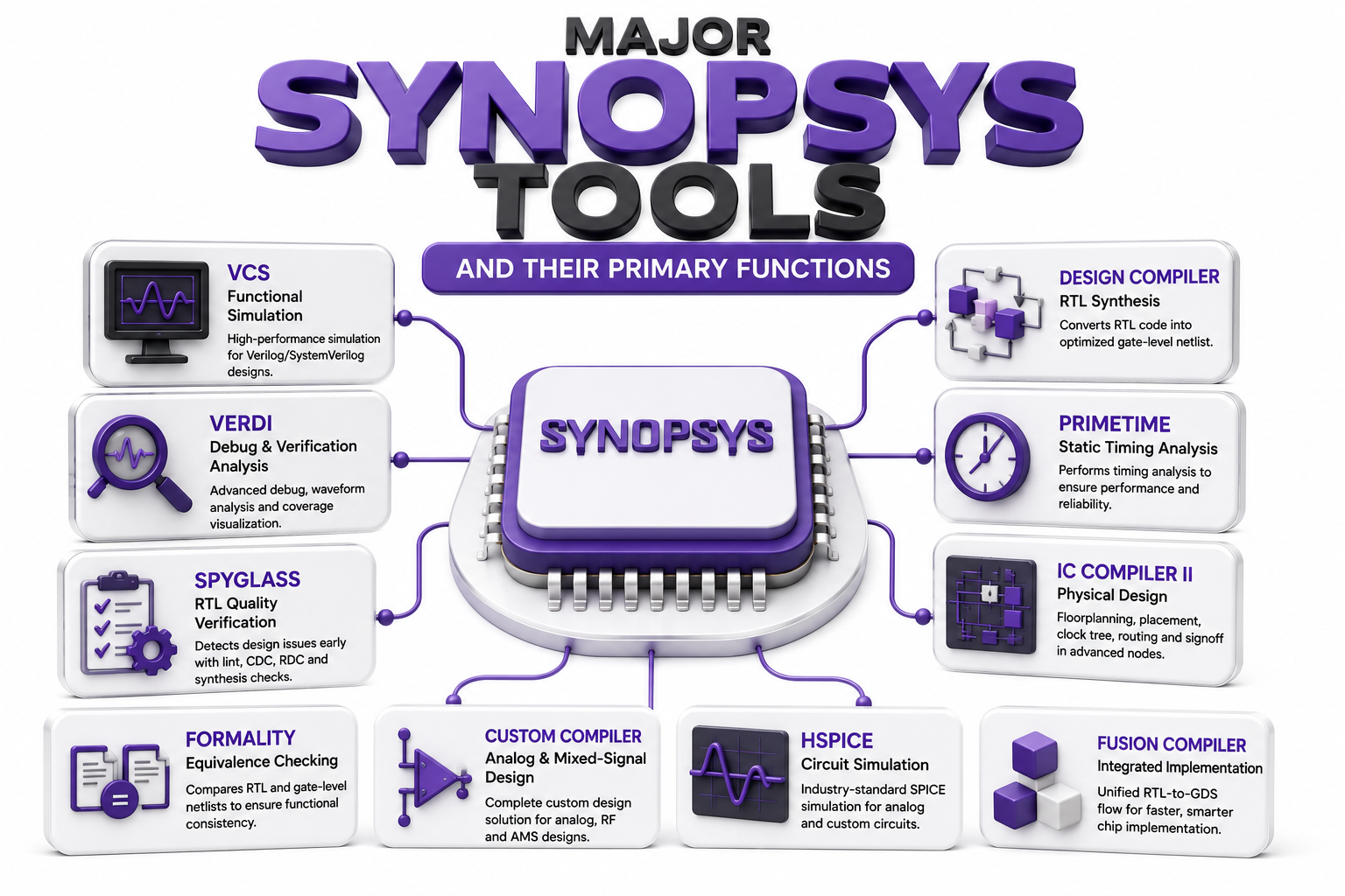
Different engineering teams rely on different Synopsys tools depending on their responsibilities throughout the design flow.
Some of the most widely used tools include:
Design Compiler for RTL synthesis
VCS for functional simulation
Verdi for debugging and waveform analysis
PrimeTime for static timing analysis
IC Compiler II for physical design
Fusion Compiler for integrated implementation
SpyGlass for RTL quality checking
Formality for equivalence checking
Custom Compiler for analog and mixed-signal design
HSPICE for transistor-level simulation
Together, these applications create a connected ecosystem where engineers can move efficiently from RTL code to manufacturing-ready layouts while maintaining design quality throughout development.
How Synopsys Tools Fit into the Complete Chip Design Flow
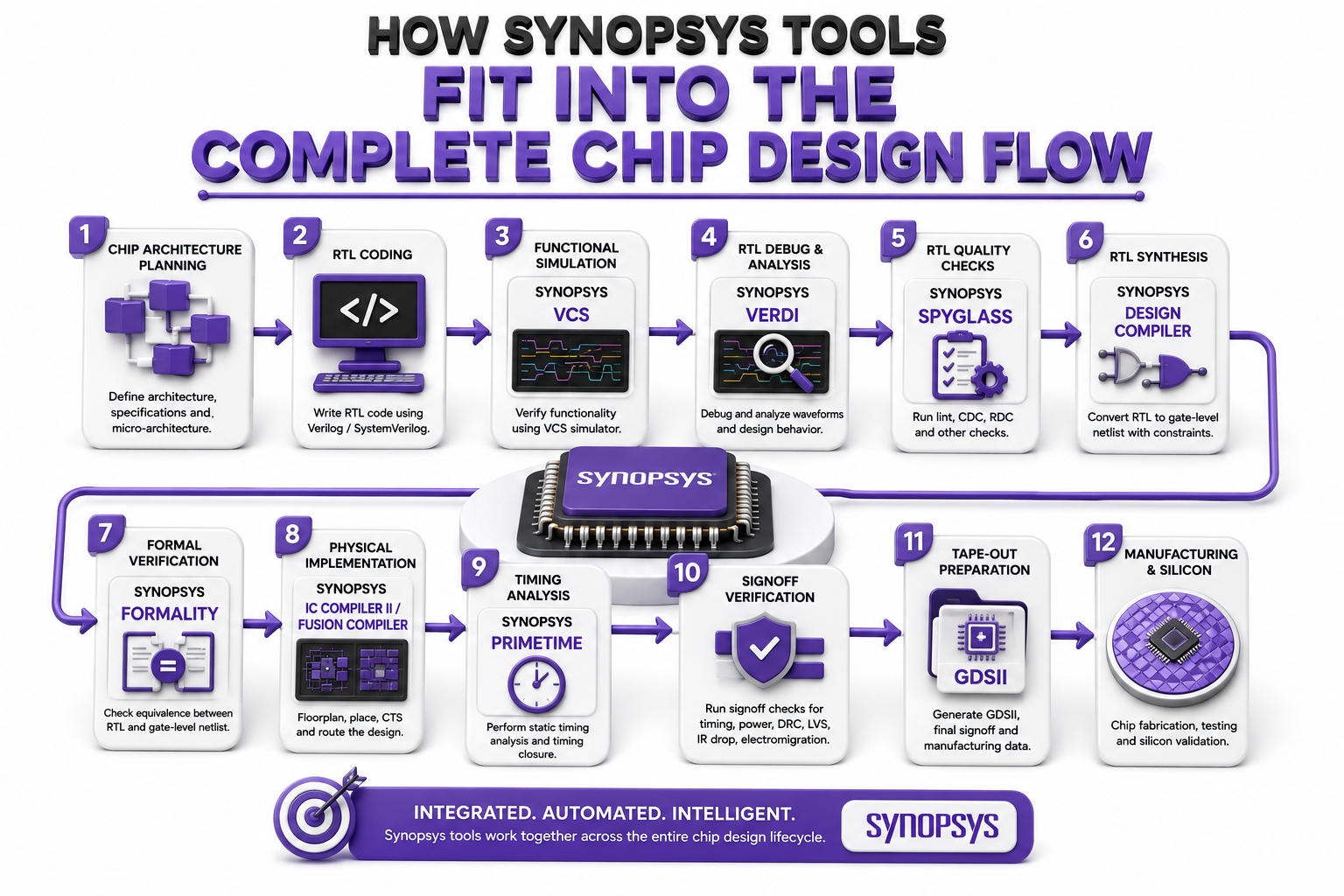
Understanding individual tools is useful, but understanding the entire workflow is even more valuable for aspiring VLSI engineers.
A simplified semiconductor design flow typically follows these stages:
Chip architecture planning
RTL coding using Verilog or SystemVerilog
Functional simulation using VCS
RTL debugging with Verdi
Lint and CDC analysis using SpyGlass
RTL synthesis through Design Compiler
Formal verification using Formality
Physical implementation using IC Compiler II or Fusion Compiler
Static timing analysis with PrimeTime
Power and signal integrity verification
Tape-out preparation
Each stage validates the previous one, ensuring that design errors are identified early before manufacturing. This integrated workflow significantly reduces project cost and improves first-silicon success rates.
Which Semiconductor Engineers Use Synopsys Tools?
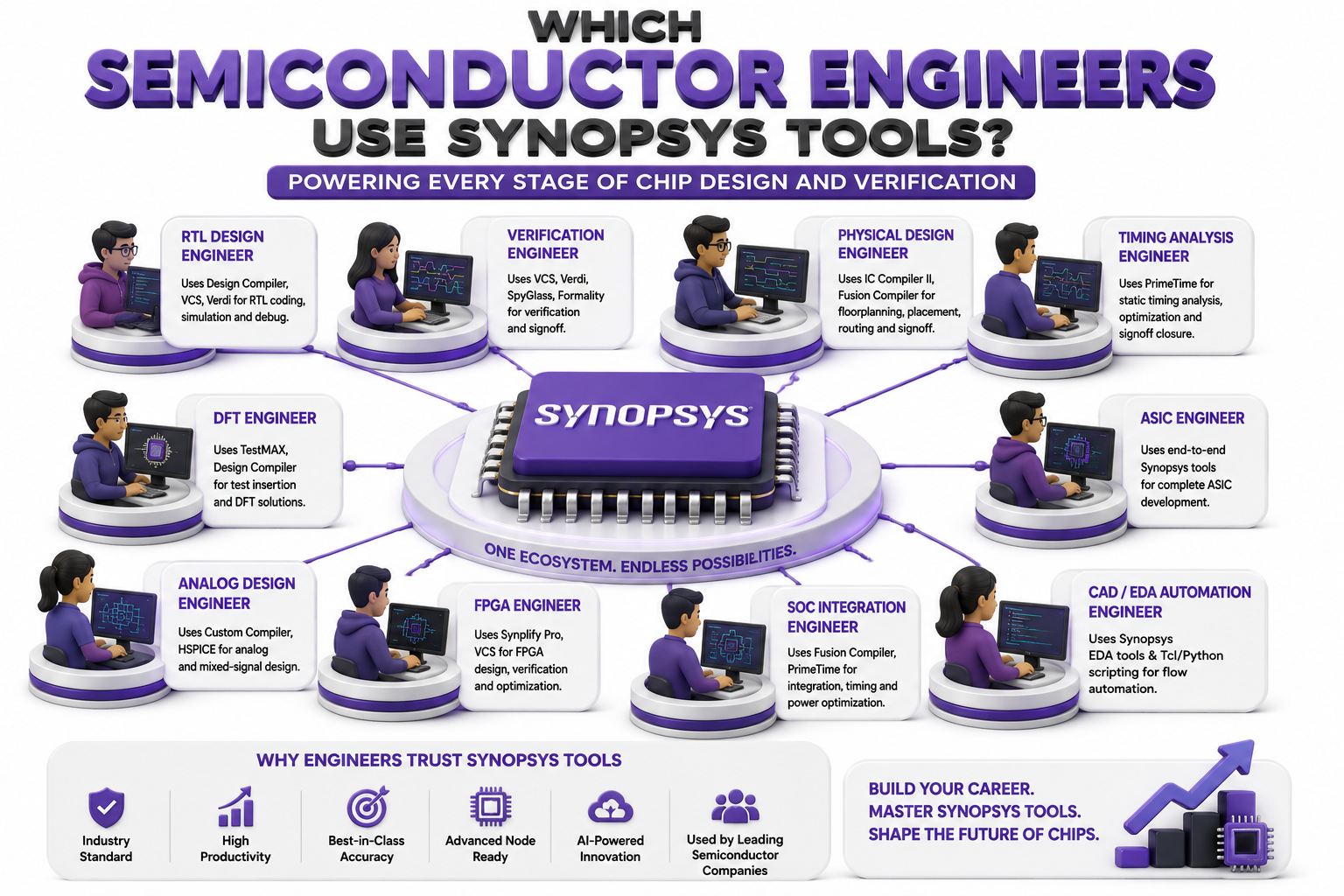
One of the reasons Synopsys skills are highly valued is their relevance across multiple semiconductor career paths. Different engineering roles interact with different parts of the EDA ecosystem depending on project requirements.
Common job roles include:
RTL Design Engineer
Verification Engineer
Physical Design Engineer
Timing Analysis Engineer
DFT Engineer
Analog IC Design Engineer
ASIC Engineer
FPGA Engineer
SoC Integration Engineer
CAD/EDA Automation Engineer
Because these tools are widely adopted by global semiconductor companies, practical experience with Synopsys software often improves employability. Training programs offered by JastTech combine theoretical concepts with hands-on exercises, helping learners understand how these tools are used in real engineering environments.
AI Is Transforming Synopsys EDA Tools in 2026

Artificial intelligence has become a major force in semiconductor design. Instead of relying solely on manual optimization, engineers now use AI-assisted workflows to accelerate design closure and improve overall chip quality.
Recent innovations include:
Automated floorplanning suggestions
AI-guided placement optimization
Faster timing closure
Intelligent routing improvements
Predictive power optimization
Machine-learning-driven verification analytics
These capabilities reduce engineering effort while enabling teams to meet aggressive performance, power, and area targets. As semiconductor designs become more complex, AI-enhanced EDA tools are expected to play an even larger role in future chip development.
How to Learn Synopsys Tools and Build a Semiconductor Career
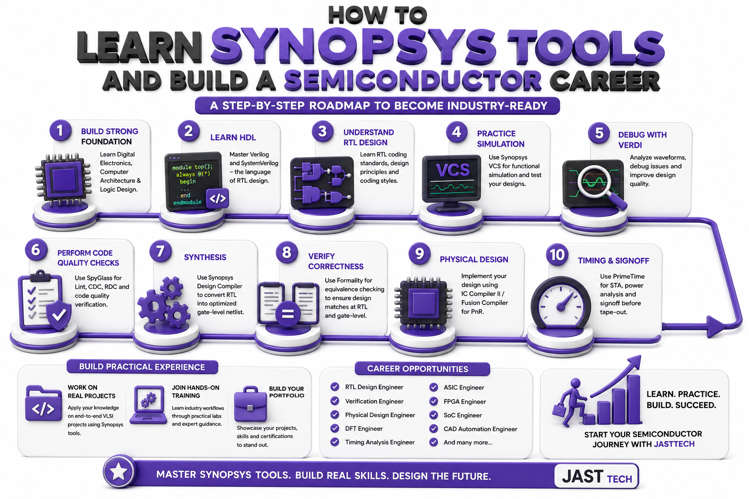
Learning every Synopsys application at once can feel overwhelming, but a structured roadmap makes the process manageable.
A recommended progression is:
Learn digital electronics fundamentals
Study Verilog and SystemVerilog
Understand RTL design principles
Practice simulation using VCS
Explore debugging with Verdi
Learn synthesis using Design Compiler
Understand timing analysis with PrimeTime
Study physical design using IC Compiler II
Build complete VLSI projects
Practice interview-focused problem solving
Hands-on learning is essential because semiconductor companies value practical experience over theoretical knowledge alone. JastTech offers industry-oriented training designed around real chip development workflows, enabling learners to gain familiarity with widely used Synopsys tools through guided projects and practical assignments.
Conclusion
Synopsys has become an essential part of the global semiconductor ecosystem by providing a comprehensive suite of Electronic Design Automation tools that support every phase of chip development. From RTL simulation and synthesis to physical implementation and timing analysis, these solutions enable engineers to build increasingly sophisticated integrated circuits with greater accuracy and efficiency. As semiconductor technologies continue advancing toward smaller process nodes and AI-driven architectures, expertise in Synopsys tools remains a valuable asset for engineers across multiple domains.
For students, fresh graduates, and working professionals aiming to enter or advance within the VLSI industry, understanding how these tools fit into the complete semiconductor workflow is just as important as learning their individual features. A structured learning path supported by practical projects and industry-focused guidance from JastTech can help bridge the gap between academic concepts and real-world engineering practices, preparing learners for the evolving demands of the semiconductor industry in 2026 and beyond.