


Top Physical Design Interview Questions and Answers for VLSI Engineers
Navigate through this article using the table of contents below
Table of Contents
No headings found in this article.
A candidate is asked what to do when hold violations show up after clock tree synthesis. Half the room says “add buffers” and stops there, while the interviewer waits for the reasoning behind it. That gap between a memorized answer and an explained one is what most physical design interview questions are built to expose, and structured physical design training helps close it.
This guide walks through the questions VLSI engineers actually face, stage by stage, with answers that show your thinking.
Physical Design Interview Questions Start With the Flow, Not the Tools

Physical design turns a gate-level netlist into a manufacturable layout, the GDSII file a foundry uses. Along the way the design passes through floorplanning, power planning, placement, clock tree synthesis, routing, and signoff checks for timing, power, and physical rules.
Interviewers rarely ask you to recite that list. They use it as a map and then pick a stage to probe. A fresher might hear, “Explain the place-and-route flow and what goes in and out of each step.” An engineer with a few years of experience is more likely to hear, “You see congestion around a macro cluster after placement. How do you debug it?” The first question checks vocabulary. The second checks judgment.
Know the inputs: the synthesized netlist, SDC timing constraints, library files such as LEF and liberty timing models, and floorplan constraints. Know the outputs too: a routed database, parasitics in SPEF format, DEF, and the final GDS. Constraints and library views drive almost every decision in the flow, which is why follow-up questions so often land there.
One habit separates strong answers from average ones: tie each step to the metric it protects. Floorplanning affects congestion and IR drop. Placement affects wirelength and timing. Clock tree synthesis affects skew and power. Routing affects crosstalk and design rule violations. When you answer in terms of the metric, you sound like someone who has seen a design fail, not someone who has read a definition.
Floorplanning and Power Planning Questions That Catch Candidates Off Guard
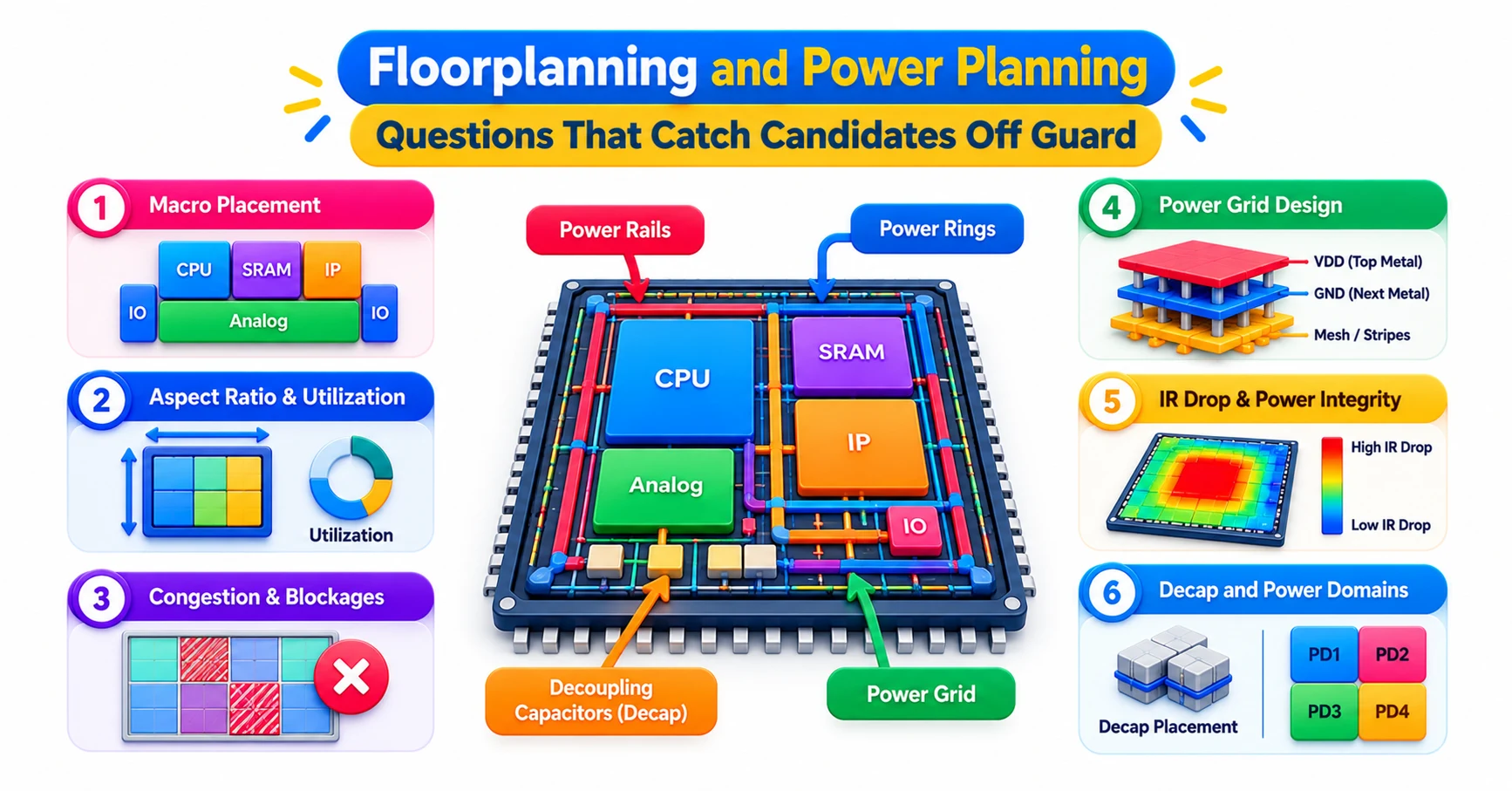
What factors decide macro placement? Start with connectivity. Macros that talk to each other heavily should sit close together, and macros that talk to the I/O pins should sit near those pins. Then mention keeping macros toward the periphery so the core stays open for standard cells, leaving enough channel space between them for routing, and orienting pins to face the logic they connect to. Blocking placement and routing halos around macros are a good detail to add.
What is core utilization, and what happens if it is too high or too low? It is the share of core area occupied by standard cells. Too high, and you get congestion, difficulty fixing timing, and no room for later ECO changes. Too low, and you waste die area and lengthen wires. Say that the right value depends on the design, the metal stack, and how many macros are present, rather than quoting a magic number.
How is power delivered across the chip? Describe the power grid: rings around the core and macros, straps on higher metal layers, and rails on the lowest layer that feed standard cells. Mention that vias connect these layers and that grid density is a trade-off between voltage drop and routing resources.
What is IR drop, and how do you reduce it? IR drop is the voltage lost across the resistance of the power network, so cells far from the supply see a lower voltage and slow down. Fixes include widening or adding straps, adding more power pads or bumps, inserting decoupling capacitors near switching hotspots, and spreading high-activity cells apart. Distinguish static IR drop from dynamic IR drop, which depends on simultaneous switching.
Also be ready to explain electromigration. Current density in thin metal can slowly move metal atoms and cause opens or shorts over the chip’s lifetime, so power wires need enough width for the current they carry.
Placement and Congestion: Answering the “Why Did This Happen?” Questions

Placement decides where every standard cell sits. Global placement spreads cells to minimize wirelength and meet timing goals roughly, then legalization snaps them onto valid rows and sites without overlaps, and detailed placement refines the result.
A common question is, “What causes congestion, and how do you fix it?” Congestion happens when the routing demand in a region exceeds the tracks available. Typical causes are high local cell density, macros that block routing layers, pin-dense cells packed together, and poor macro orientation. Fixes depend on the cause. You might lower utilization locally with placement blockages, increase cell padding around dense regions, move or rotate macros, enable congestion-driven placement, or revisit the floorplan if the problem is structural.
Interviewers also like, “What is the difference between timing-driven and wirelength-driven placement?” Wirelength-driven placement only tries to shorten total wire. Timing-driven placement uses slack information to pull cells on critical paths closer together, even if that costs some wirelength elsewhere.
Expect a question on what happens in pre-CTS optimization: buffering long nets, resizing cells, fixing max transition and max capacitance violations, and cloning or splitting high-fanout nets. The clock is still ideal at this point, so setup timing looks better than it will after the clock tree is built. Saying this out loud shows you understand why results change between stages.
A beginner mistake worth avoiding is treating a high congestion map as a routing problem. Often it is a floorplan or placement problem that routing merely reveals, and strong candidates say so. Another is fixing overflow by lowering utilization globally when only one corner of the die is hot.
Clock Tree Synthesis Questions on Skew, Latency, and Useful Skew
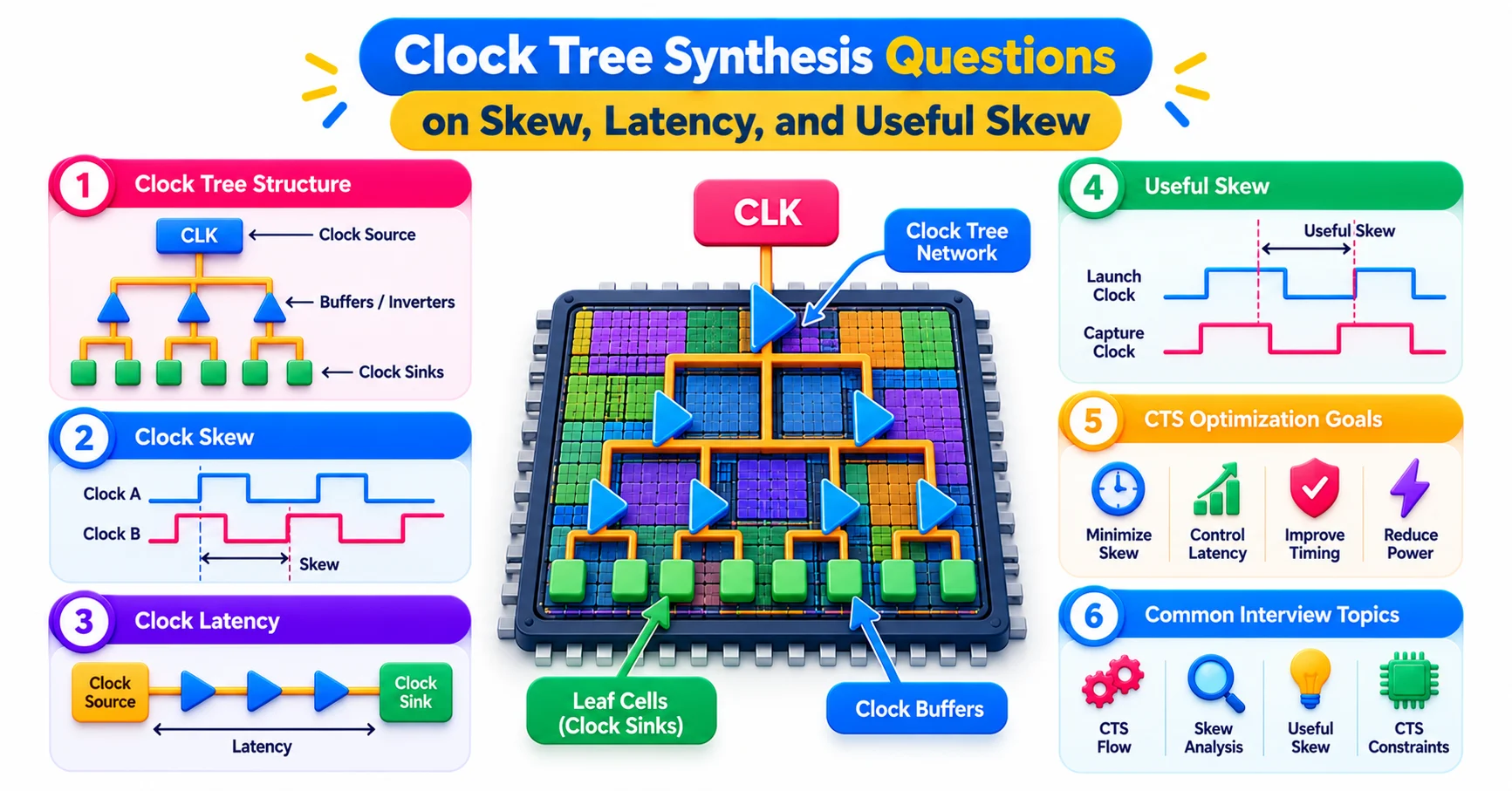
Clock tree synthesis, or CTS, builds the network that delivers the clock to every sequential element. The goals are low skew, controlled latency, acceptable power, and robustness against variation.
What is clock skew? It is the difference in clock arrival time between two flip-flops. Skew is not always bad. Positive skew in the right direction can help setup on a path and hurt hold, while the opposite direction does the reverse. That leads naturally to useful skew, where the tool or the engineer deliberately delays or advances a clock to borrow time for a critical path.
What is insertion delay, or latency? It is the delay from the clock source to a flip-flop’s clock pin. Large latency increases exposure to on-chip variation and power consumption in the tree.
Interviewers often ask why clock nets get special treatment. Because the clock toggles every cycle and reaches thousands of sinks, it uses non-default routing rules such as wider wires and extra spacing, and sometimes shielding, to reduce resistance and crosstalk. Be ready to compare a standard buffered tree with an H-tree and a clock mesh, noting that meshes lower skew and variation but cost much more power and routing resource.
Two more topics appear often. Clock gating saves dynamic power by stopping the clock to idle logic, and gating cells must be placed so the enable timing is met. Common path pessimism removal, or CRPR, removes the artificial pessimism that arises when launch and capture clock paths share part of the same physical route.
If asked what you check after CTS, list skew, latency, transition on clock pins, duty cycle, and then re-run setup and hold analysis, since both change once the clock is real.
Static Timing Analysis Questions Every Physical Design Engineer Must Handle
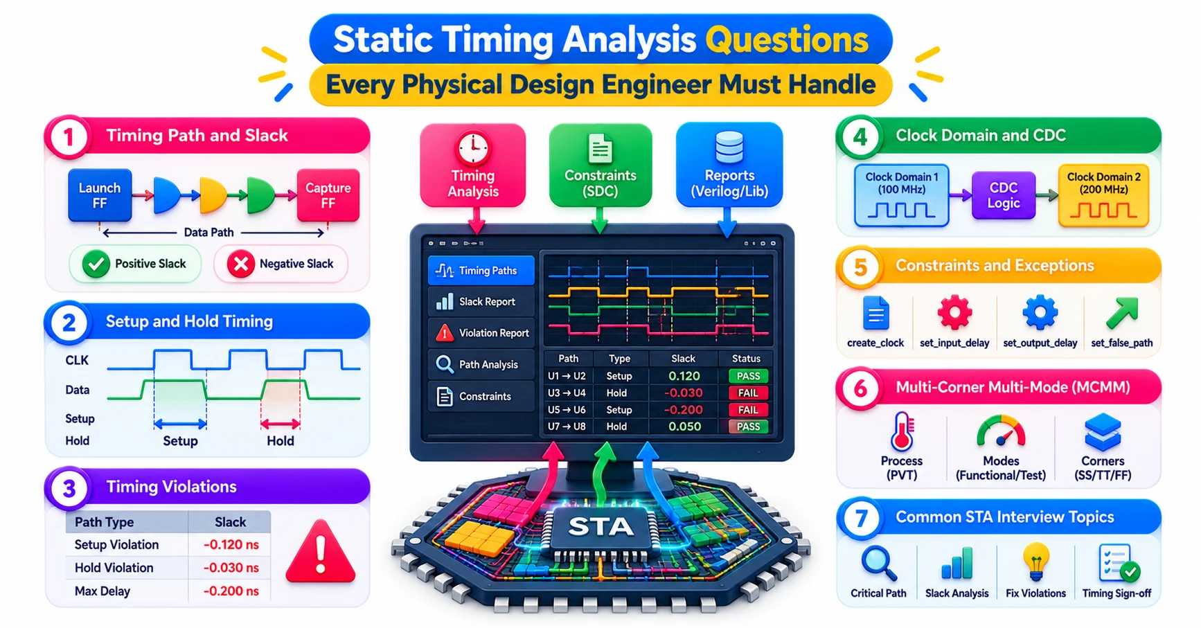
Timing questions are where interviews are won or lost. Start with the definitions. Setup time is how long data must be stable before the capturing clock edge. Hold time is how long it must stay stable after the edge. Slack is the margin between required and actual arrival time, and negative slack is a violation.
How do you fix setup violations? Reduce the delay on the failing path. Upsize drivers, swap cells to a lower threshold voltage where leakage budget allows, insert or remove buffers, reduce logic depth through restructuring, shorten wires by improving placement, promote critical nets to faster metal layers, or apply useful skew.
How do you fix hold violations? Add delay to the short path, usually with delay cells or buffers, or reduce the delay of the capture clock. Fix hold after setup is mostly clean, because delay added for hold can break setup. Mention that hold violations do not depend on clock frequency, so slowing the clock does not help, a point many candidates miss.
Expect questions on variation. On-chip variation models the fact that two nearby cells may not behave identically. Advanced approaches such as AOCV and POCV apply derates based on path depth and statistical spread, which is less pessimistic than a flat derate. Multi-corner multi-mode analysis checks the design across process, voltage, and temperature corners and across functional and test modes.
You should also explain false paths and multicycle paths. A false path never gets exercised functionally, so it should not be timed. A multicycle path is one where data is allowed more than one clock cycle to arrive. Mention that wrongly applied exceptions can hide real failures, which is why they need careful review.
Routing, Signal Integrity, and Physical Verification Questions

Routing connects all pins with metal and vias while following design rules. It usually runs in stages: global routing plans the rough paths, track assignment places wires on tracks, and detailed routing finishes exact geometry and fixes violations.
What is crosstalk? It is unwanted coupling between neighboring wires. A switching aggressor can slow down or speed up a victim, which creates delay changes in timing and, in bad cases, glitches that corrupt logic. Fixes include spacing wires apart, shielding critical nets, buffer insertion, upsizing the victim driver, and changing layers.
What is the antenna effect? During manufacturing, long metal pieces collect charge in plasma etching steps and can damage thin gate oxide connected to them. Typical fixes are inserting antenna diodes near the gate, breaking the wire with a jumper on a higher layer, or using layer hopping so the exposed metal area stays small.
Physical verification questions follow routing:
DRC checks geometric rules such as minimum width, spacing, and enclosure.
LVS compares the layout against the schematic or netlist to confirm they describe the same circuit.
ERC looks for electrical issues like floating nets or shorted power and ground.
A good candidate can explain what causes common DRC failures, such as dense via arrays or tight spacing near macros, and how metal fill is added to meet density rules and improve manufacturability.
Finally, expect an ECO question. An engineering change order is a late, small modification, such as fixing a timing violation or a functional bug, made without redoing the whole flow. Explain that the goal is to change as few cells and wires as possible, using spare cells or filler space, then re-verify timing and rules.
Turning Knowledge Into Answers: How to Prepare for the Interview Itself

Knowing the concepts is only half the work. Interviewers listen for how you structure an answer, so practice a pattern: define the term in one sentence, explain why it matters, give the cause or mechanism, then name the fix and its trade-off. This fits nearly every question above.
Scenario questions deserve their own practice. “Setup fails on 200 paths after routing, where do you start?” has no single answer. A good response looks at whether violations cluster on one block or clock domain, checks for a constraint or clock issue before touching the layout, and only then moves to optimization. Showing a debugging order impresses more than naming five tricks.
Tool familiarity helps, but concepts travel across them. Whether a team uses Innovus, IC Compiler II, or PrimeTime, interviewers care that you understand what a command does, not just its spelling. If you have worked on a block or a small design, even in training, describe it with specifics: the technology node used in the exercise, the problems you hit, and what you changed. Programs such as the ones JastTech runs for physical design learners are useful mainly because they give you a project to talk about, and an honest project story carries more weight than a list of buzzwords.
Avoid common mistakes: memorizing numbers without context, claiming experience with a step you cannot explain, and giving one-word answers to open questions. When you do not know something, say how you would find out.
Conclusion
Physical design interview questions reward clear thinking more than recall. If you can follow a design from floorplan to signoff and explain what each stage protects, most follow-up questions become conversations instead of quizzes. Keep practicing with real scenarios, and your answers will start sounding like experience.