

Understanding Industry Expectations for Physical Design Engineers: Insights from JastTech
Navigate through this article using the table of contents below
Table of Contents
No headings found in this article.
Getting a physical design job requires more than understanding VLSI concepts. Semiconductor companies expect engineers to translate theoretical knowledge into reliable, optimized chip layouts. But what separates an ordinary candidate from an industry-ready physical design engineer?
As semiconductor technology advances, hiring expectations are also changing. Companies increasingly value practical implementation, timing closure, debugging, and problem-solving abilities. Understanding these expectations is the first step toward building a successful career in physical design.
Understanding the Complete Physical Design Flow
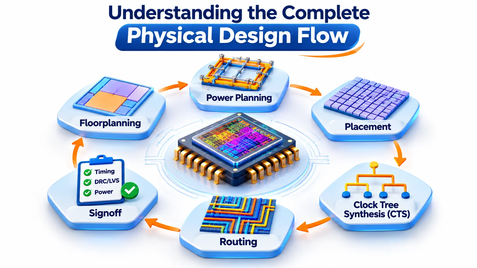
One of the most important expectations companies have is a strong understanding of the complete physical design process. Engineers must know how a synthesized netlist becomes a manufacturable layout through multiple implementation and optimization stages.
The physical design flow generally includes:
Floorplanning: Defining the core area, aspect ratio, macro placement, and placement blockages.
Power Planning: Creating power rings, stripes, and power distribution networks.
Placement: Positioning standard cells while considering timing, congestion, and power.
Clock Tree Synthesis (CTS): Building a clock distribution network to control skew and insertion delay.
Routing: Establishing physical connections between cells and other design components.
Signoff: Performing timing, physical verification, and power-integrity checks before tapeout.
Companies expect engineers to understand not only what happens at each stage but also how decisions in one stage affect subsequent stages.
For example, poor macro placement during floorplanning can create routing congestion later. Similarly, aggressive placement optimization can improve timing but increase power consumption or routing complexity.
At JastTech, developing a strong understanding of this complete flow is an important part of preparing aspiring engineers for practical semiconductor projects.
Strong Fundamentals in STA and Timing Closure
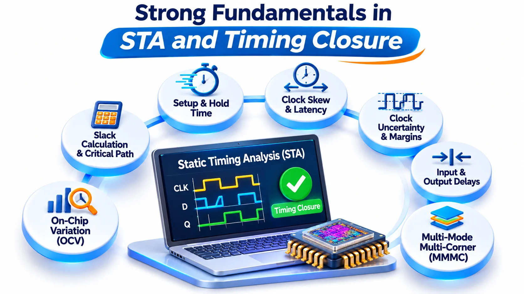
Static Timing Analysis (STA) is one of the most important technical areas for physical design engineers. Semiconductor companies expect candidates to understand how timing constraints influence implementation and how timing violations can be identified and resolved.
Engineers should understand:
Setup and hold time requirements.
Clock skew and clock latency.
Clock uncertainty and timing margins.
Input and output delay constraints.
Slack calculation and critical path identification.
Multi-Mode Multi-Corner (MMMC) analysis.
On-Chip Variation (OCV) concepts.
Understanding setup and hold violations is particularly important.
A setup violation occurs when data arrives too late at the capture register. Common corrective approaches include cell upsizing, buffering, placement optimization, and reducing routing delays.
A hold violation occurs when data arrives too early. Engineers may introduce delay buffers or make other implementation changes to satisfy minimum-delay requirements.
However, companies do not simply expect engineers to memorize these solutions. They want candidates who can examine timing reports, identify the actual problem, understand its root cause, and select an appropriate correction without creating additional violations.
Practical knowledge of timing closure is therefore a major advantage during technical interviews and professional project assignments.
Hands-On Experience With Industry EDA Tools
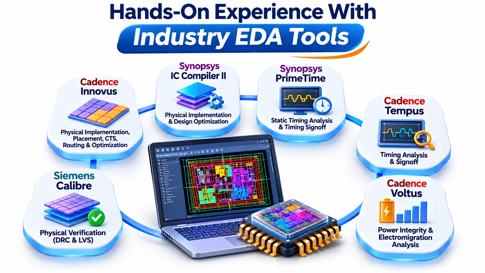
Understanding physical design concepts is essential, but companies also expect engineers to work with Electronic Design Automation (EDA) tools.
These tools help engineers implement, optimize, analyze, and verify complex semiconductor designs.
Some commonly used industry tools include:
Cadence Innovus: Physical implementation, placement, CTS, routing, and optimization.
Synopsys IC Compiler II: Physical implementation and design optimization.
Synopsys PrimeTime: Static timing analysis and timing signoff.
Cadence Tempus: Timing analysis and signoff.
Cadence Voltus: Power integrity and electromigration analysis.
Siemens Calibre: Physical verification, including DRC and LVS workflows.
Companies generally value candidates who understand the purpose of these tools and can navigate their implementation workflows.
However, knowing tool commands alone is not enough. Engineers must understand why particular commands are used, how to interpret generated reports, and how to troubleshoot implementation problems.
This is where practical Physical Design Training becomes valuable. Working on implementation exercises helps learners connect theoretical concepts with actual tool behavior.
Engineers should also become comfortable with Linux environments because semiconductor design workflows frequently involve command-line operations, file management, and execution of automated scripts.
Problem-Solving Skills in PPA Optimization and Physical Verification
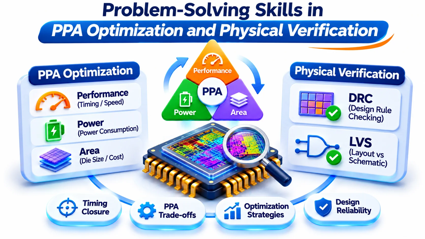
Modern semiconductor projects require engineers to optimize Power, Performance, and Area (PPA) while maintaining design reliability and manufacturability.
Companies expect physical design engineers to understand the relationship between these three parameters.
For example, increasing cell drive strength may improve timing but increase area and power consumption. Similarly, inserting additional buffers may reduce transition violations while increasing congestion and dynamic power.
Engineers must evaluate these trade-offs instead of concentrating on only one optimization target.
Another important expectation is the ability to identify and resolve physical design violations.
Common implementation challenges include:
Congestion: Too many routing connections competing for limited routing resources.
IR Drop: Voltage reduction caused by resistance in the power delivery network.
Electromigration: Metal degradation caused by excessive current density.
Crosstalk: Unwanted coupling between neighboring signal nets.
DRC Violations: Layout geometry failing to meet manufacturing design rules.
LVS Mismatches: Differences between the intended circuit connectivity and the extracted layout connectivity.
Companies expect engineers to understand the causes of these problems and identify appropriate corrective actions.
For instance, congestion may require macro repositioning, cell spreading, or floorplan modifications. IR drop may require power-grid optimization, additional power resources, or improvements to current distribution.
An engineer who understands these relationships can contribute more effectively to real implementation projects.
Scripting, Automation, and Cross-Team Collaboration
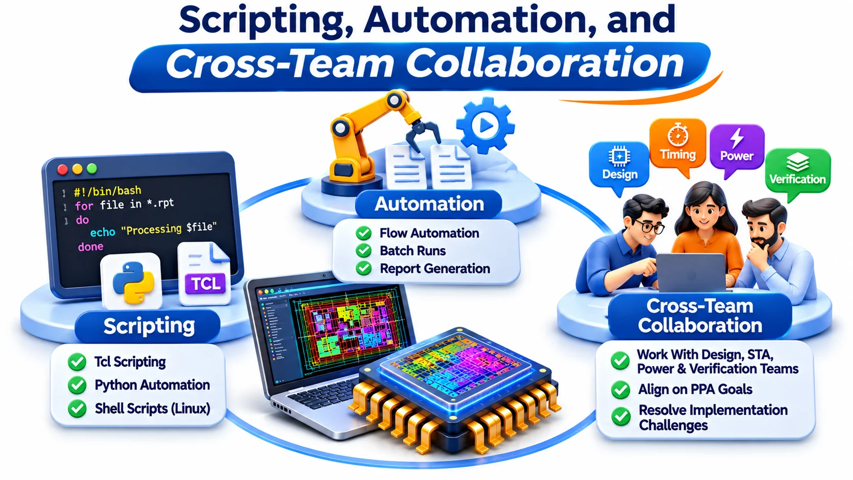
Physical design engineers regularly work with large designs that generate substantial amounts of implementation data and reports. Manually analyzing everything is inefficient.
Consequently, scripting and automation have become valuable professional skills.
Engineers should develop familiarity with:
Tcl: Automating EDA tool operations and implementation workflows.
Python: Processing reports, analyzing data, and creating automation utilities.
Linux Shell: Managing files, executing scripts, and working with design environments.
For example, a Python script can extract timing violations from multiple reports and organize them according to slack values. Tcl can automate repetitive implementation commands and generate customized reports.
Beyond technical automation, companies also expect engineers to collaborate with different semiconductor engineering teams.
Physical design professionals regularly interact with:
RTL design engineers.
Synthesis engineers.
Design verification engineers.
Static timing analysis engineers.
DFT engineers.
Physical verification and signoff teams.
These interactions are important because physical implementation problems can originate from decisions made during earlier design stages.
Engineers must communicate technical issues clearly, explain optimization decisions, document debugging activities, and coordinate changes with relevant teams.
Strong communication and teamwork help ensure that implementation activities remain aligned with overall project requirements.
How Aspiring Engineers Can Become Industry-Ready With JastTech
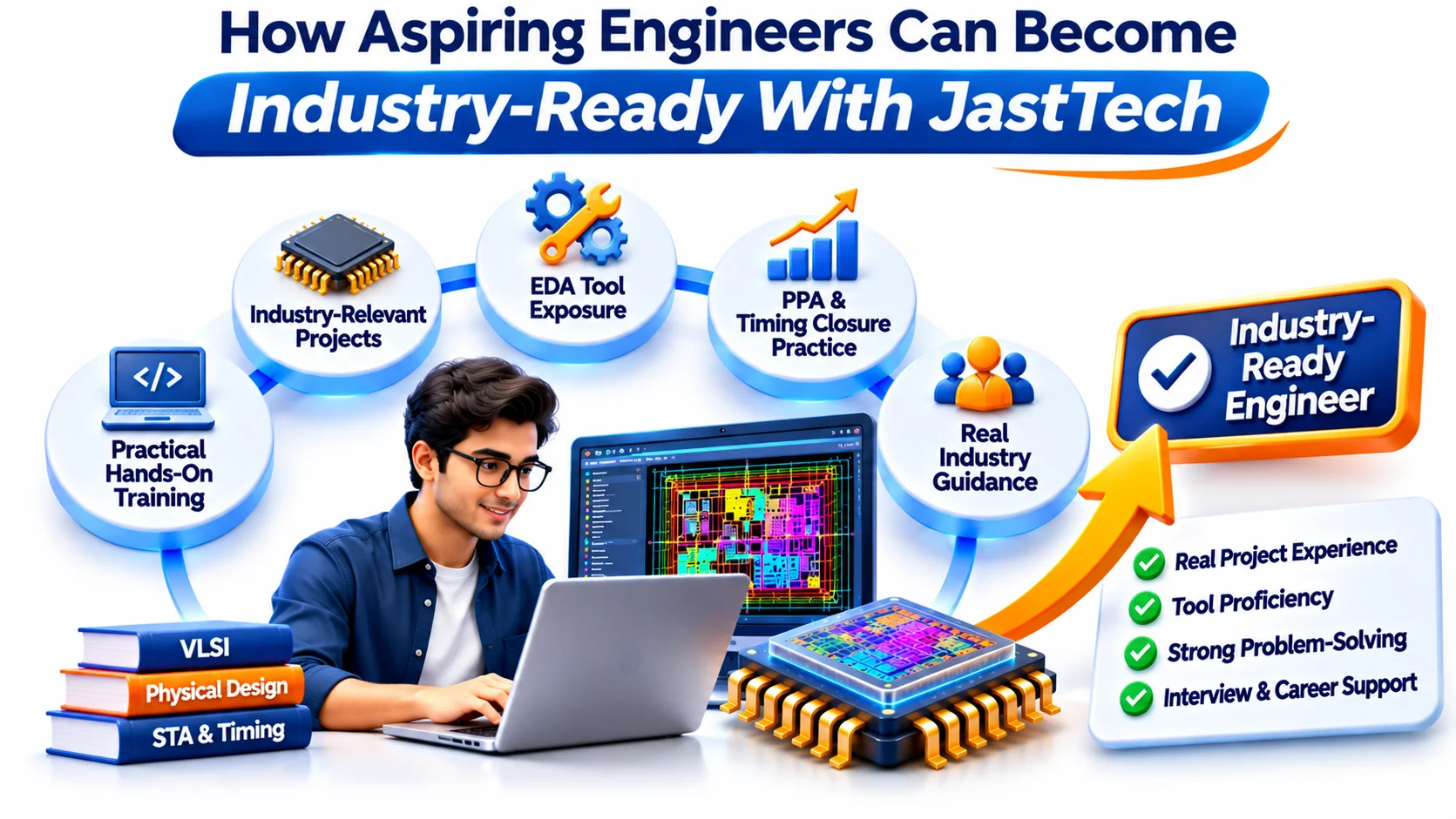
Understanding industry expectations is only the beginning. Aspiring physical design engineers must convert their knowledge into practical abilities that demonstrate their readiness for semiconductor projects.
A structured learning approach should focus on building technical fundamentals before progressing toward complex implementation activities.
JastTech emphasizes the importance of practical learning and industry-oriented skill development for aspiring VLSI professionals.
Engineers preparing for physical design careers should concentrate on the following areas:
Build Digital Electronics Fundamentals: Understand logic gates, flip-flops, combinational circuits, sequential circuits, and timing concepts.
Learn the Physical Design Flow: Study every stage from synthesized netlist to GDSII and understand the purpose of each activity.
Develop STA Knowledge: Practise setup and hold calculations, timing report interpretation, and timing optimization.
Gain EDA Tool Exposure: Understand implementation workflows using industry-standard physical design tools.
Work on Practical Projects: Perform floorplanning, placement, CTS, routing, and basic signoff activities wherever suitable tool access is available.
Prepare for Technical Interviews: Practise scenario-based questions involving congestion, timing violations, IR drop, and physical verification.
A useful way to demonstrate practical knowledge is through a project portfolio. Candidates should be able to explain the design inputs, implementation stages, optimization decisions, encountered problems, and final results.
For freshers, understanding the reasoning behind implementation decisions is often more valuable than simply memorizing tool commands.
JastTech aims to help learners build this practical foundation and understand the technical expectations associated with professional VLSI physical design roles.
Conclusion
The expectations for physical design engineers extend far beyond understanding floorplanning, placement, CTS, and routing. Semiconductor companies look for professionals who can combine strong fundamentals, EDA tool knowledge, timing analysis, PPA optimization, scripting, and practical debugging abilities. Engineers who understand how individual implementation decisions affect overall chip performance are better prepared to contribute to demanding semiconductor projects.
Building these capabilities requires consistent practice, structured learning, and exposure to real-world implementation challenges. Through industry-oriented learning and practical skill development, JastTech helps aspiring engineers understand what companies expect and prepare for opportunities in the semiconductor industry. Investing in the right technical skills today can create a stronger foundation for a successful physical design career.