

VLSI Salary in Hyderabad 2026 HITEC City vs Gachibowli Companies
Navigate through this article using the table of contents below
Table of Contents
No headings found in this article.
A VLSI engineer working in Hyderabad can earn dramatically more than another engineer with similar years of experience. The surprising part is that location alone rarely explains the difference. In 2026, specialization, company category, project ownership and engineering depth increasingly determine what appears on the offer letter.
That makes the HITEC City vs Gachibowli comparison more interesting than simply asking which area pays more. Both sit inside Hyderabad's powerful technology corridor, but the opportunities surrounding them can differ by employer, engineering function and type of semiconductor work. Here is how engineers should evaluate the market.
Hyderabad's VLSI Salary Market Is Wider Than a Single Average
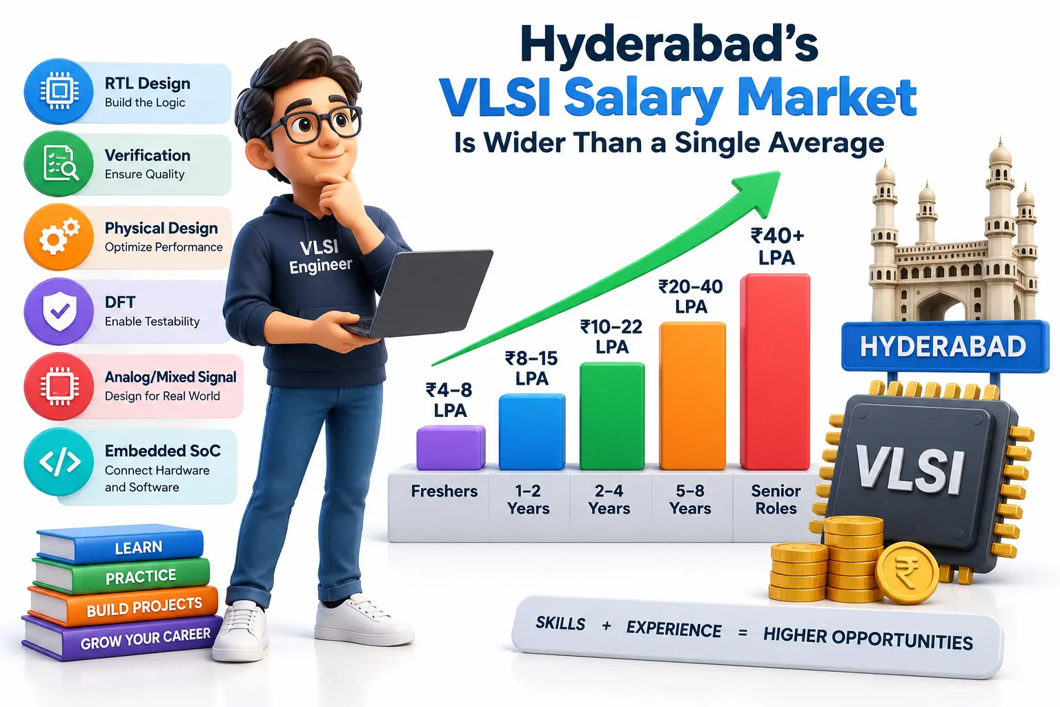
Searching for the average VLSI salary in Hyderabad can be misleading because “VLSI engineer” covers several completely different engineering careers. An RTL engineer, verification engineer, physical design engineer and DFT engineer may have similar experience but very different compensation.
For 2026, a practical market-oriented expectation can be viewed broadly as:
Freshers and entry-level engineers: approximately ₹4–8 LPA in many service, training-to-employment and smaller engineering organizations
Strong product-company entry roles: approximately ₹8–15+ LPA depending on skills and hiring standards
Engineers with 2–4 years: approximately ₹10–22+ LPA
Engineers with 5–8 years: approximately ₹20–40+ LPA
Highly specialized senior engineers: ₹40 LPA and above can become possible in selected product, semiconductor and leadership roles
These are indicative bands rather than guaranteed salaries. A candidate's domain, employer, educational background, interview performance and ability to handle production-level engineering can move compensation significantly.
The important lesson is therefore not to ask, “What is the Hyderabad VLSI salary?” Ask, “What does my specific engineering profile command in Hyderabad?”
HITEC City Remains a Powerful Technology Employment Corridor
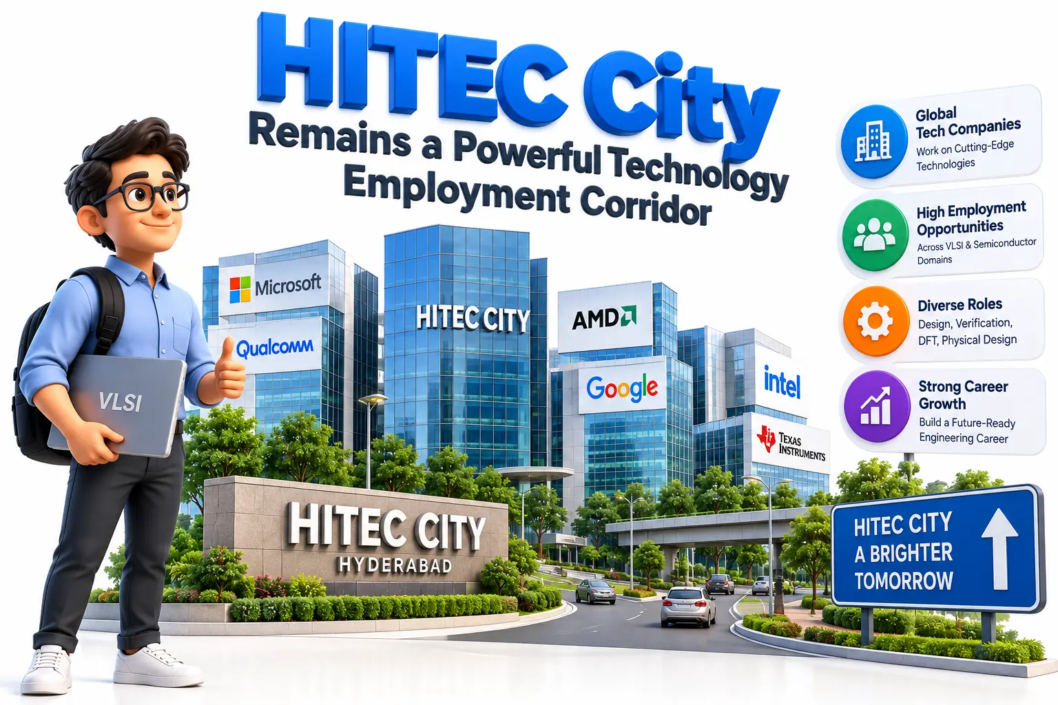
HITEC City and the surrounding Madhapur–Raidurg technology belt have long been associated with Hyderabad's technology ecosystem. The area gives engineers access to large technology organizations, engineering centers, service companies, startups and multinational operations.
For VLSI candidates, its biggest advantage is not a magical HITEC City salary premium. It is the density of technology employment around the western Hyderabad corridor. Engineers can encounter opportunities involving semiconductor design as well as embedded systems, firmware, EDA, hardware-software integration and adjacent engineering functions.
Compensation here depends heavily on the employer model. A semiconductor product organization hiring an experienced verification engineer can operate with a very different salary structure from an engineering-services company hiring for customer projects.
When evaluating an opportunity around HITEC City, examine:
Whether the employer develops products or provides engineering services
Whether you work directly for a semiconductor organization or on a client project
Technical ownership given to the engineering team
Fixed salary versus bonus, stock and other benefits
Technologies, nodes and project complexity involved
Opportunities to move into senior technical positions
The company and role usually matter considerably more than the office pin code.
Gachibowli Can Compete Directly for High-Value Engineering Talent
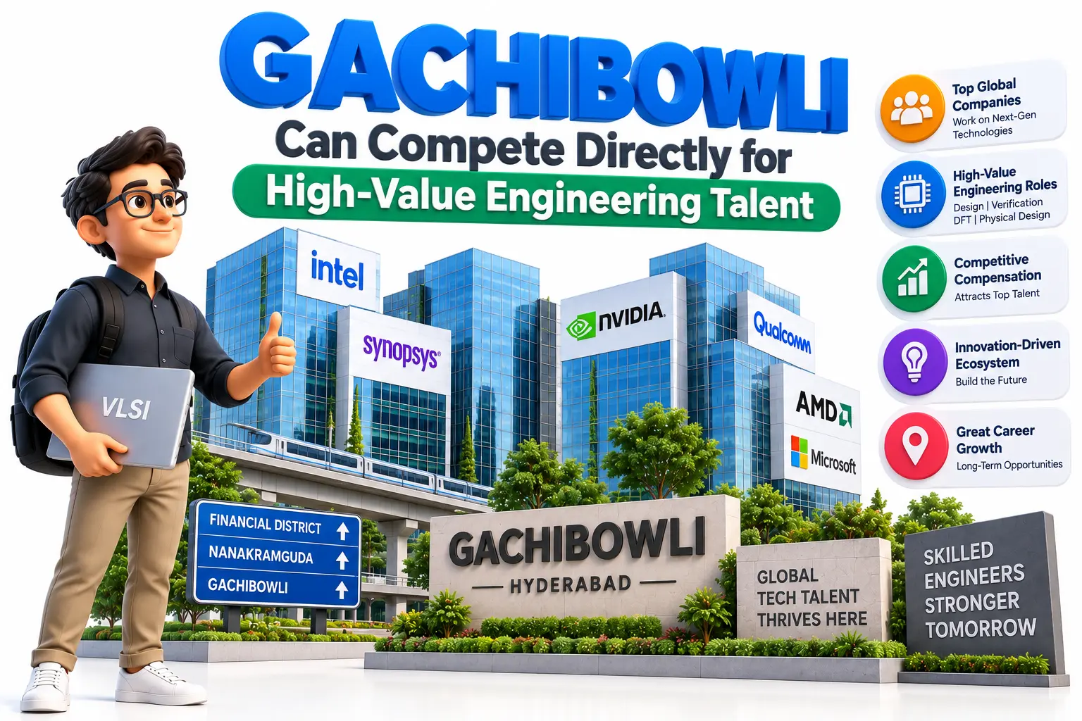
Gachibowli and the adjoining Financial District–Nanakramguda corridor have become major destinations for multinational technology and global capability operations. Consequently, engineers should not treat Gachibowli as a secondary option compared with HITEC City.
For experienced semiconductor professionals, the real competition happens at the employer level. Companies requiring scarce RTL, SoC verification, timing, physical design or DFT expertise may pay aggressively regardless of whether their office is labelled Gachibowli, Nanakramguda, Madhapur or another nearby technology district.
This is why comparing two job offers requires looking beyond CTC. Consider:
Base compensation and variable pay
Joining or retention bonuses
Equity or stock benefits where applicable
Technical role and actual project ownership
Learning opportunities
Promotion structure
Commute and hybrid-work expectations
Long-term value of the technology you will work on
An ₹18 LPA position offering deep product experience could potentially strengthen future career value more than a ₹20 LPA position dominated by repetitive support work. Salary matters, but engineering exposure can influence the next three salary jumps.
Your VLSI Domain Can Matter More Than HITEC City vs Gachibowli
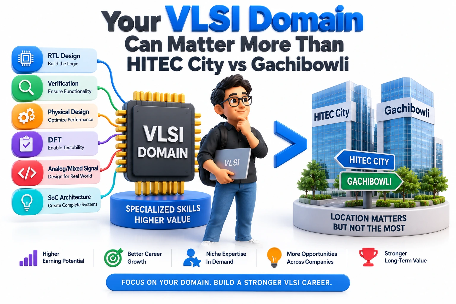
The strongest salary differentiator is frequently specialization. Companies do not simply pay for “VLSI knowledge”; they pay engineers who can solve difficult problems inside a specific part of the semiconductor development flow.
RTL engineers can improve their market value through strong digital design, Verilog/SystemVerilog, microarchitecture, synthesis awareness, timing fundamentals and CDC understanding. Verification engineers benefit from SystemVerilog, UVM, assertions, coverage, debugging and protocol knowledge. Physical design engineers need expertise extending from floorplanning and placement through CTS, routing, STA and timing closure.
DFT professionals can differentiate themselves through scan architecture, ATPG, memory testing, test coverage and silicon-test understanding. Engineers researching Synopsys Tools Used in the Semiconductor Industry should similarly understand that knowing a tool's interface is less valuable than understanding the engineering problem the tool is helping solve.
This distinction is important for freshers. Simply adding EDA tool names to a resume does not automatically create salary leverage. Employers are more interested in whether candidates can interpret results, identify failures, debug problems and explain engineering decisions.
Freshers Need to Build Salary Leverage Before Negotiating Salary
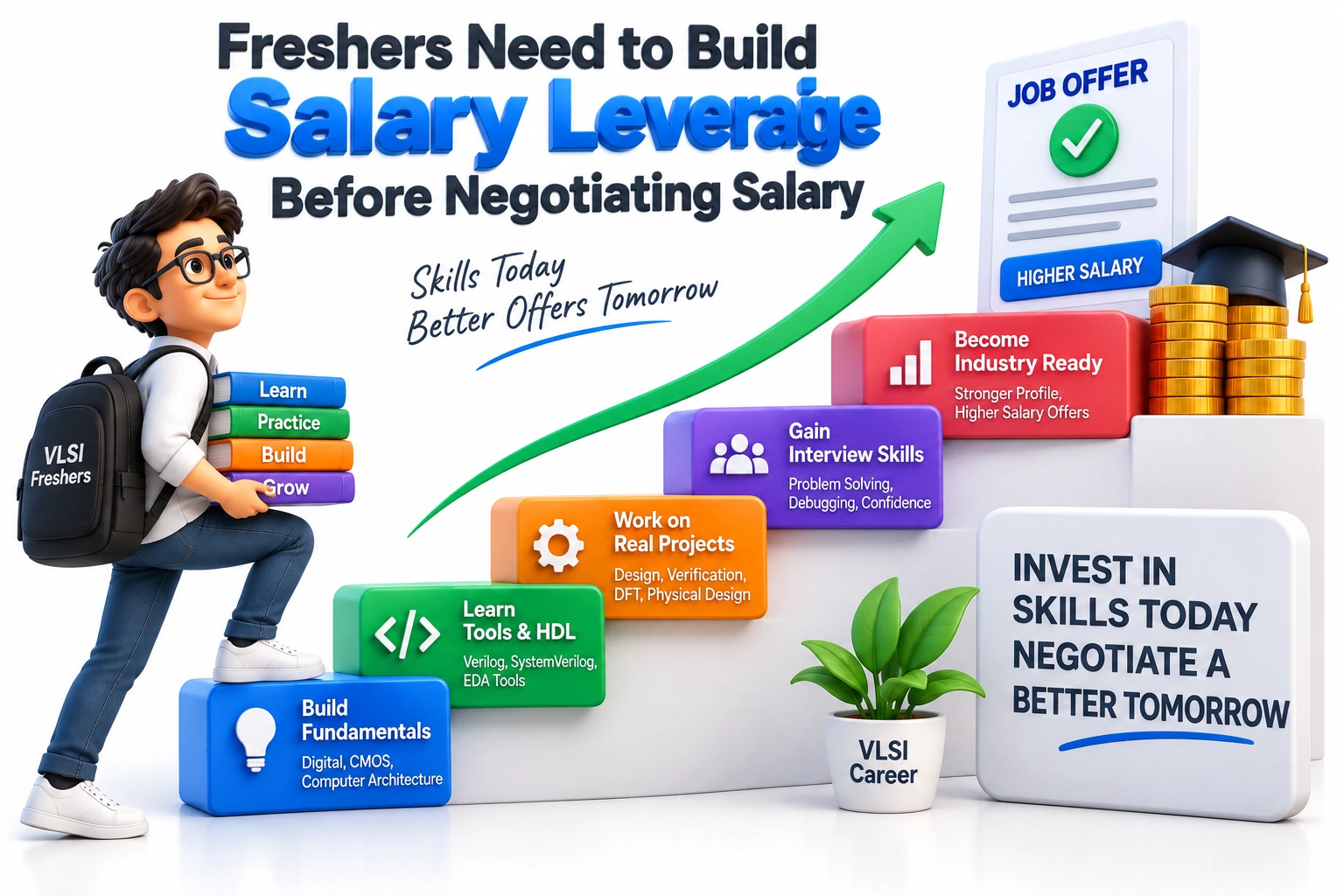
Fresh graduates naturally focus on package comparisons, but their first priority should be becoming employable for genuine engineering roles. Entry-level compensation varies substantially because the skill difference between two graduates can be surprisingly large.
A candidate who only understands definitions may compete for basic entry opportunities. Another candidate who can design an FSM, write synthesizable RTL, create a verification environment, debug waveforms and explain timing violations enters the interview with stronger evidence of ability.
Students evaluating a vlsi training institute in hyderabad should therefore look beyond advertisements built around placement packages. Practical labs, experienced mentors, project depth, debugging exercises and interview preparation are more important indicators of whether training can contribute to employability.
JastTech emphasizes the industry-readiness approach because semiconductor hiring ultimately tests application rather than certificate collection. Freshers should build their profile around:
Strong digital electronics fundamentals
One clearly selected VLSI specialization
Verilog and SystemVerilog where relevant
Practical projects they can defend technically
Debugging ability
Scripting fundamentals
Timing and semiconductor-flow awareness
Structured technical interview preparation
The objective is not simply completing a syllabus. It is becoming capable of demonstrating engineering thinking during interviews.
Build Your 2026 Salary Strategy Around Skills, Not Location Labels

For engineers comparing HITEC City and Gachibowli opportunities, the smartest approach is to evaluate career capital alongside immediate compensation. Hyderabad's western technology corridor is interconnected enough that neighborhood labels should not dominate the decision.
Instead, evaluate every opportunity using three questions: What will I learn? What will I own? What will this experience make me worth after two or three years?
A fresher may benefit from accepting a reasonable package when the role provides genuine RTL, verification, DFT or physical-design exposure. A mid-level engineer should become more selective about project complexity and technical ownership. Senior engineers should examine architecture responsibilities, leadership opportunities, specialized expertise and total compensation.
Salary growth in VLSI is rarely created by years of experience alone. Engineers who repeatedly deepen valuable capabilities can separate themselves from professionals whose resumes show years but little expansion in responsibility.
For 2026, therefore, the HITEC City vs Gachibowli question has a more useful answer than simply declaring one location the winner. Both can provide access to valuable semiconductor and technology opportunities. The better location is where the better engineering role exists for your specialization.
Conclusion
Hyderabad's VLSI opportunity is becoming increasingly skill-driven. Freshers should focus on entering the right technical track, while experienced professionals should evaluate specialization, ownership, employer quality and total compensation rather than chasing a neighborhood-based salary assumption.
The engineers likely to gain the strongest long-term returns will be those who treat their careers like semiconductor design itself: optimize the fundamentals first, identify the real bottleneck and improve continuously. HITEC City or Gachibowli may determine where you work, but your engineering depth will have a much greater influence on what you can earn.