

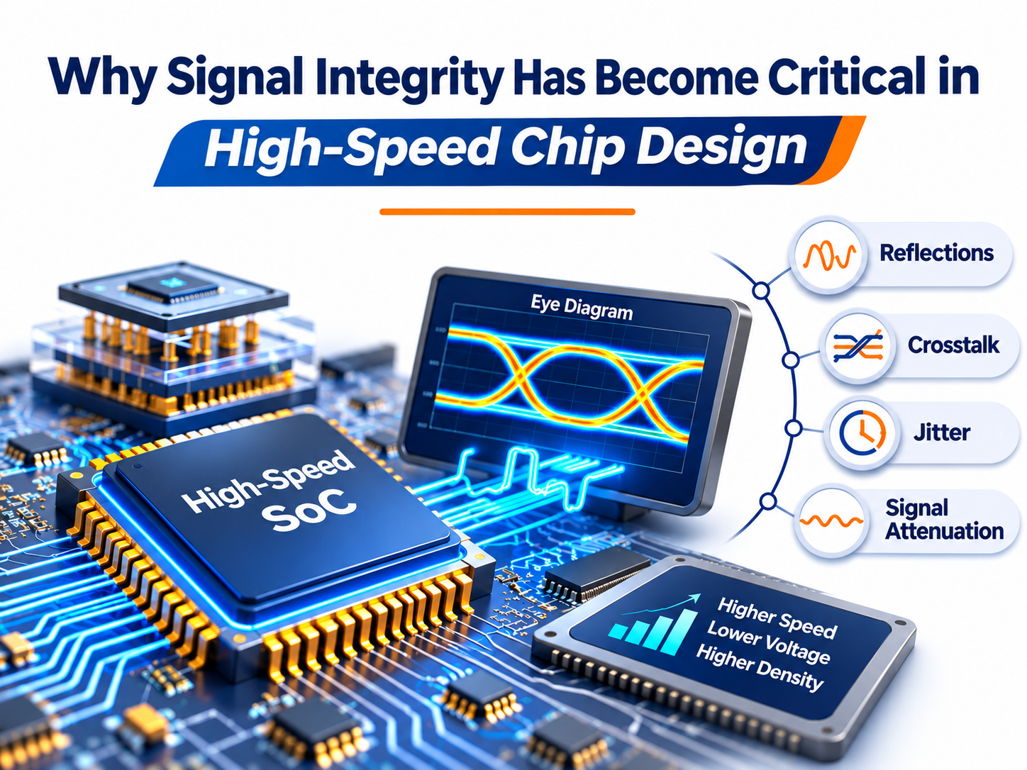
Why Signal Integrity Has Become Critical in High-Speed Chip Design
Navigate through this article using the table of contents below
Table of Contents
No headings found in this article.
Modern chips are becoming faster, smaller, and more powerful, but there is a hidden challenge behind this progress: maintaining clean and reliable electrical signals. Even a small disturbance can affect communication, timing, and overall chip performance.
As semiconductor technology advances toward high-speed interfaces, advanced packaging, and chiplet architectures, signal integrity is no longer an optional design consideration. It has become a fundamental requirement for building reliable and high-performance electronic systems.
Understanding Signal Integrity in Modern Chip Design
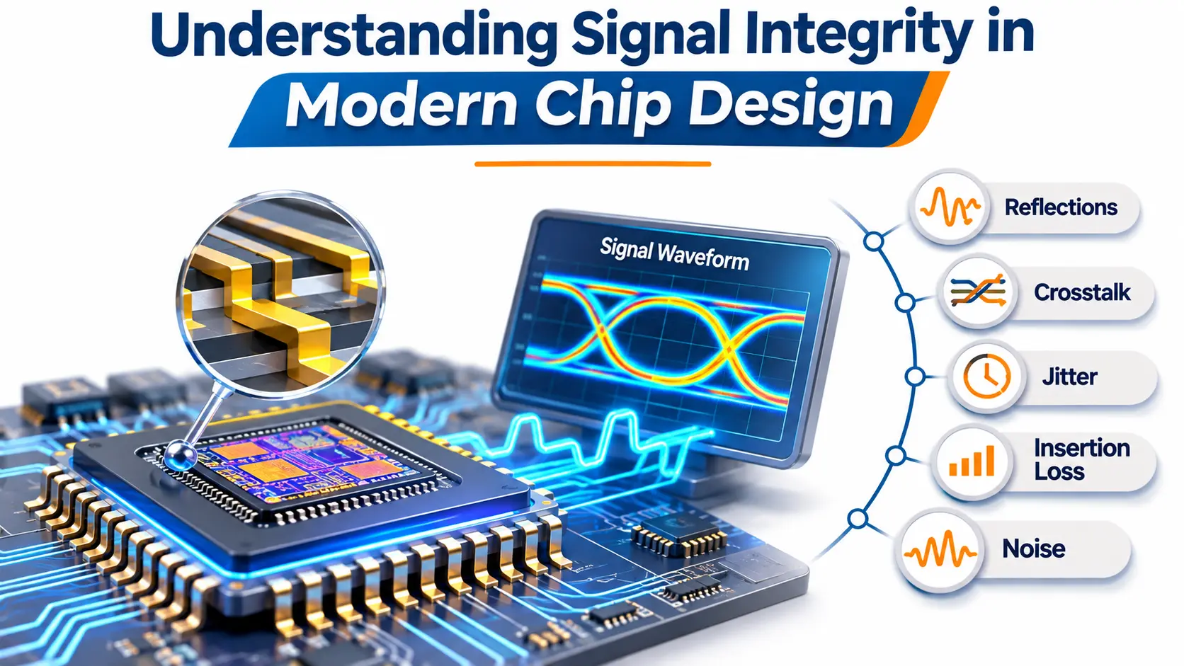
Signal integrity (SI) refers to the ability of an electrical signal to travel from its source to its destination without experiencing unacceptable distortion, noise, or degradation. In digital circuits, signals represent binary information through voltage transitions between logic levels.
Ideally, a signal should reach its destination with the correct voltage, timing, and waveform characteristics. However, real-world interconnects introduce resistance, capacitance, and inductance, which can change the behavior of electrical signals.
Signal integrity becomes particularly important when designing processors, memory controllers, communication interfaces, and high-performance SoCs.
Consider a high-speed digital interface transmitting data between two components. If the transmitted waveform becomes distorted, the receiving circuit may interpret a logic 1 as a logic 0 or detect a transition at the wrong time.
Important signal-integrity parameters include:
Signal reflections: Occur when impedance mismatches cause part of the signal to travel back toward its source.
Crosstalk: Unwanted electromagnetic coupling between neighboring signal paths.
Jitter: Variation in the timing of signal transitions.
Insertion loss: Reduction in signal amplitude as it travels through an interconnect.
Noise: Unwanted electrical disturbances that affect signal quality.
Understanding these effects helps engineers develop circuits that operate reliably under demanding conditions.
Why Increasing Chip Speeds Make Signal Integrity More Important
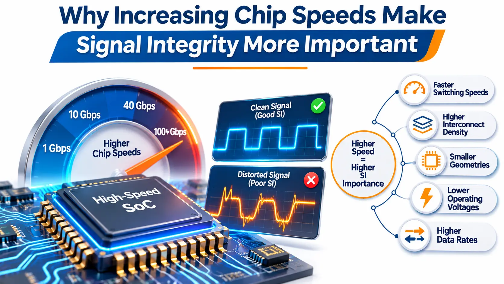
The demand for higher processing performance has significantly increased data-transfer requirements. Modern processors, AI accelerators, GPUs, and networking devices must exchange enormous amounts of information within extremely short time intervals.
As data rates increase, electrical signals become more sensitive to interconnect characteristics. Importantly, the relevant factor is not just clock frequency but also signal rise and fall times. Even a relatively low-frequency digital signal with very fast transitions can experience transmission-line effects.
Several factors make signal integrity increasingly challenging:
Faster switching speeds: Shorter transition times increase the frequency content of digital signals.
Higher interconnect density: Closely spaced wires increase electromagnetic coupling and crosstalk.
Smaller geometries: Advanced semiconductor processes introduce tighter physical design constraints.
Lower operating voltages: Reduced voltage margins make circuits more sensitive to electrical noise.
Higher data rates: Modern interfaces require accurate signal transmission within increasingly demanding timing budgets.
For example, a high-speed memory interface must transfer data reliably between the processor and memory devices. Poor signal quality can cause setup or hold violations, communication errors, and reduced operating margins.
This is why signal integrity analysis must become part of the design process rather than something engineers consider only after implementation.
Major Signal Integrity Challenges in High-Speed Chips
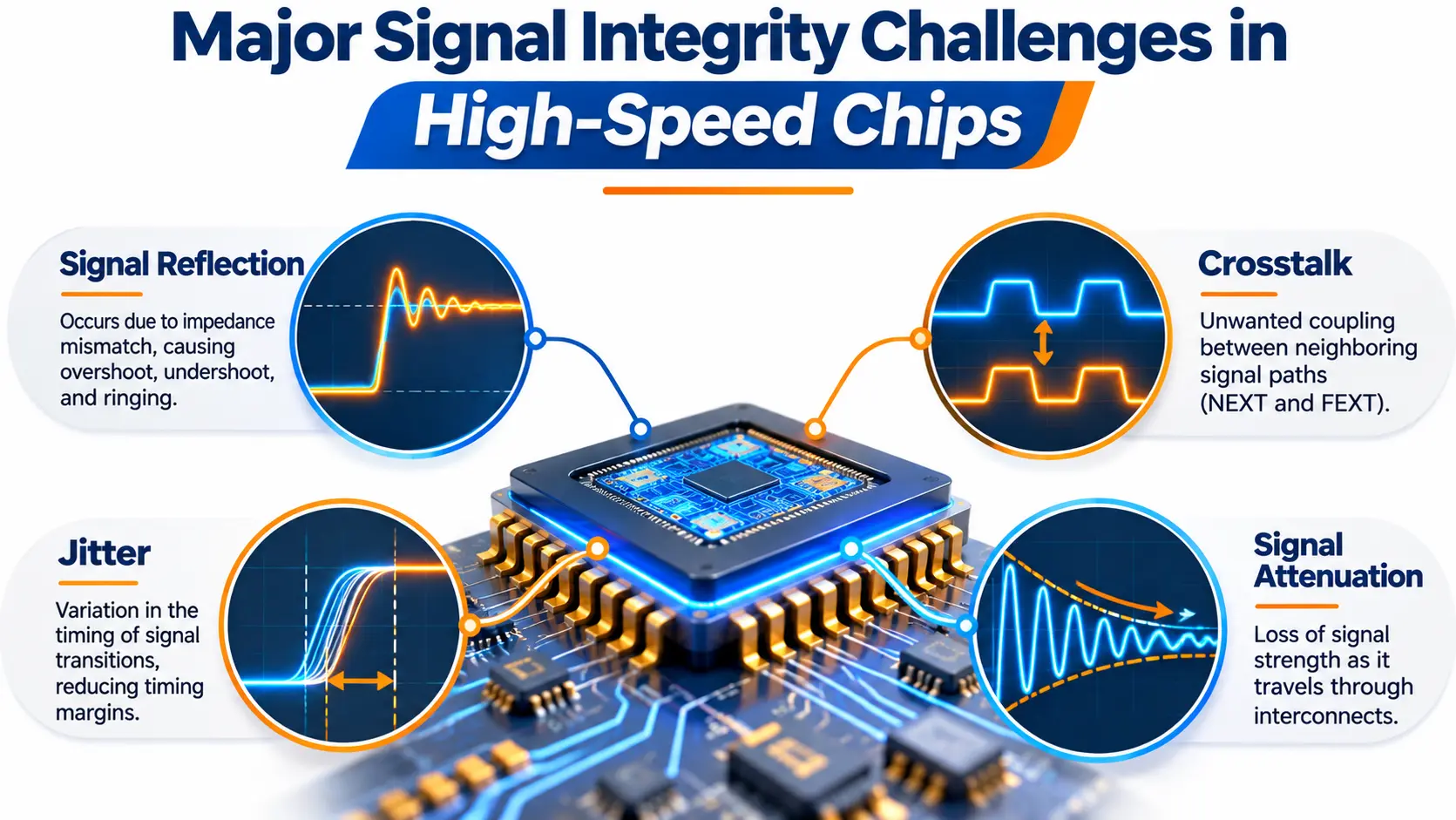
Several electrical effects can negatively influence signal quality. Engineers must understand these problems to identify potential failures before manufacturing.
Signal Reflection: Reflection occurs when an electrical signal encounters an impedance discontinuity along its transmission path. This can happen because of incorrect termination, routing changes, vias, or package transitions.
Reflected signals may create overshoot, undershoot, and ringing, potentially causing incorrect logic detection.
Crosstalk: When two signal paths run close together, electromagnetic fields from one interconnect can influence the neighboring interconnect.
Crosstalk is commonly classified into:
Near-end crosstalk (NEXT): Interference measured near the source end of the affected line.
Far-end crosstalk (FEXT): Interference measured near the receiving end.
Jitter: Jitter affects the timing accuracy of digital signals. Excessive jitter reduces the available sampling window and can increase bit error rates in high-speed communication systems.
Signal Attenuation: Electrical signals lose energy while traveling through interconnects because of conductor resistance, dielectric losses, and frequency-dependent effects.
These problems can become more severe in high-density designs where numerous high-speed signals operate simultaneously.
The Relationship Between Signal Integrity, Power Integrity, and Timing
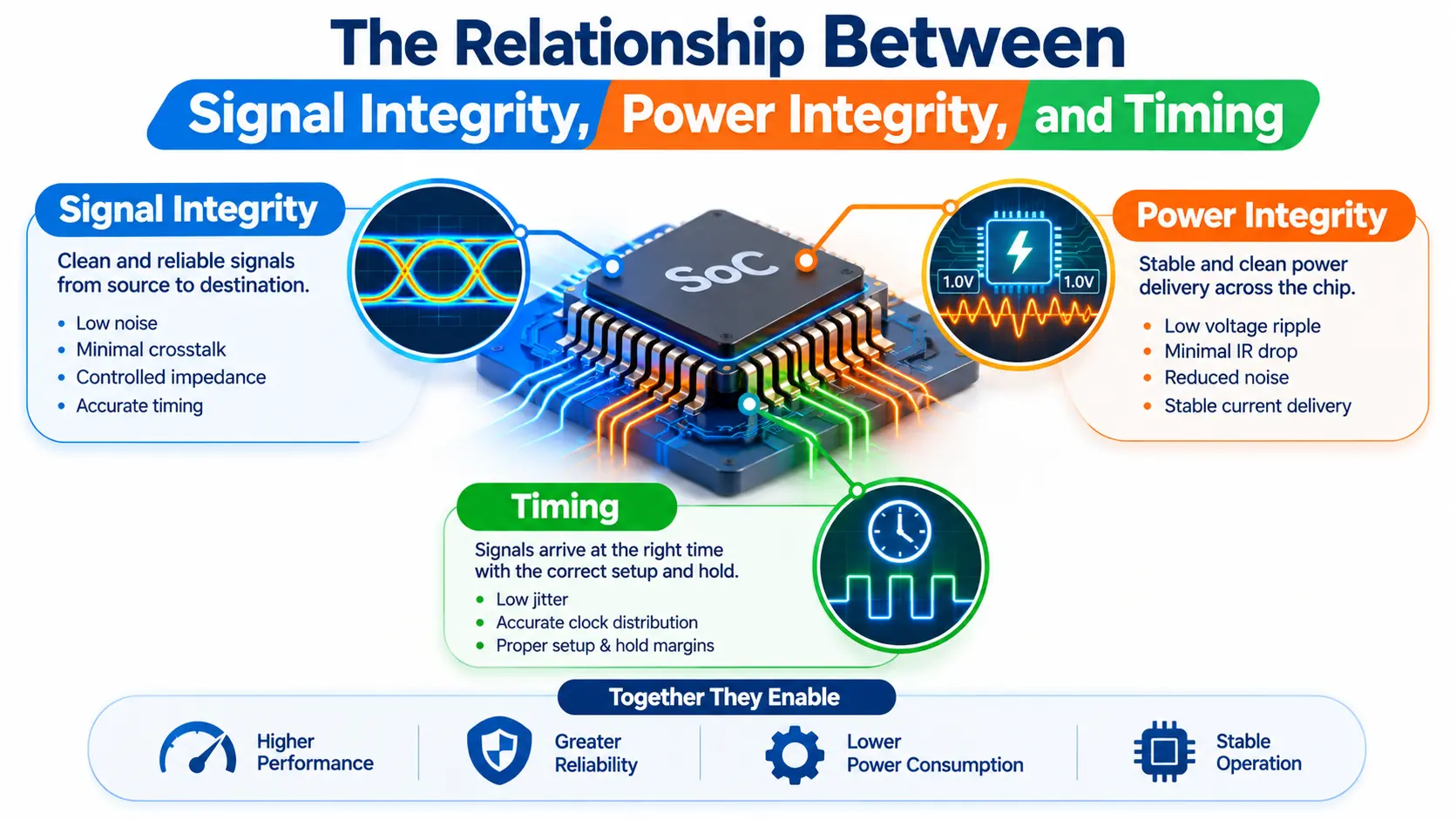
Signal integrity, power integrity, and timing are closely connected aspects of modern semiconductor design. An issue in one area can directly influence the performance of another.
Power integrity focuses on delivering stable voltage and current to different circuit blocks. When multiple transistors switch simultaneously, sudden current demands can create voltage fluctuations across the power distribution network.
These fluctuations may introduce supply noise, ground bounce, and simultaneous switching noise (SSN), affecting signal quality and circuit behavior.
Timing analysis is equally important because digital circuits must receive valid signals within specified timing windows.
For example, excessive signal delay or jitter can reduce the available setup margin at a receiving register. Similarly, supply-voltage fluctuations can change transistor switching characteristics and affect circuit delay.
Engineers therefore consider several important factors:
Setup time: The minimum time data must remain stable before the active clock edge.
Hold time: The minimum time data must remain stable after the active clock edge.
Clock uncertainty: Accounts for clock-related variations, including applicable jitter and skew components.
Voltage fluctuations: Can affect propagation delay and switching behavior.
Noise margins: Determine how much electrical disturbance a circuit can tolerate.
For students exploring semiconductor careers, understanding these relationships is valuable. A VLSI Training Institute in Hyderabad should emphasize the connection between digital fundamentals, timing analysis, and physical implementation rather than teaching these subjects as completely separate concepts.
How Engineers Analyze and Improve Signal Integrity
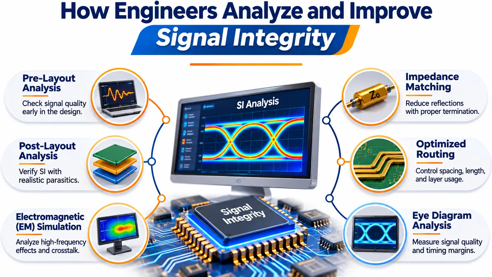
Signal integrity problems must be identified early because correcting them after manufacturing can increase development costs and delay product releases.
Modern semiconductor engineering teams use a combination of design guidelines, modeling, simulation, and measurement techniques to maintain signal quality.
A typical engineering approach includes:
Pre-Layout Analysis: Engineers evaluate expected interconnect behavior using preliminary models and identify potential impedance, timing, and coupling problems.
Post-Layout Analysis: Extracted parasitic information from the physical layout is used to understand the electrical behavior of actual interconnect structures.
Electromagnetic Simulation: Advanced simulation techniques help evaluate complex interconnect geometries, coupling effects, and frequency-dependent behavior.
Eye Diagram Analysis: Engineers examine signal quality by overlaying multiple received waveforms. An open eye generally indicates better timing and voltage margins, while a closing eye indicates increasing distortion or noise.
Time-Domain and Frequency-Domain Analysis: Time-domain analysis helps evaluate waveform behavior, while frequency-domain analysis provides information about channel characteristics, insertion loss, and return loss.
Common techniques for improving signal integrity include:
Maintaining controlled impedance along high-speed signal paths.
Using appropriate termination techniques to minimize reflections.
Maintaining continuous reference planes and reliable return paths.
Optimizing differential-pair routing and coupling.
Reducing unnecessary vias and interconnect discontinuities.
Evaluating power distribution networks to minimize supply noise.
Engineers working in RTL Design and Verification Training in India can also benefit from understanding these physical design considerations because RTL functionality eventually needs to operate within real electrical and timing constraints.
Why Signal Integrity Skills Matter for the Future of VLSI Engineering
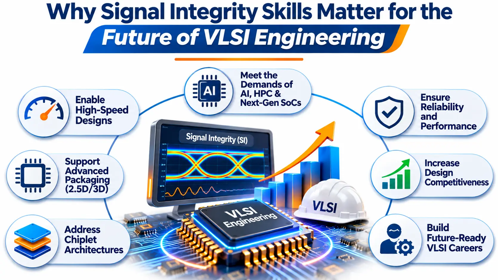
The semiconductor industry is moving toward increasingly complex architectures. AI processors, high-bandwidth memory, advanced networking chips, and chiplet-based systems require reliable communication between multiple components.
In chiplet architectures, different dies communicate through dense interconnect structures using advanced packaging technologies. These connections introduce additional electrical challenges involving channel loss, crosstalk, impedance discontinuities, and power delivery.
Technologies such as 2.5D and 3D integration make signal integrity analysis increasingly important because engineers must evaluate electrical behavior across multiple interconnected dies.
This creates opportunities for engineers with knowledge of:
Digital electronics and CMOS fundamentals.
Static timing analysis and timing constraints.
Physical design and parasitic extraction.
High-speed interfaces and transmission-line fundamentals.
Signal integrity and power integrity analysis.
Semiconductor verification and debugging.
JastTech recognizes the importance of practical semiconductor knowledge in preparing engineers for industry requirements. Learning how digital circuits interact with real physical interconnects helps students develop a broader understanding of modern chip development.
Signal integrity is no longer limited to specialized high-speed interface teams. Its principles influence architecture, circuit design, physical implementation, package engineering, and system-level validation.
Conclusion
Signal integrity has become critical in high-speed chip design because modern semiconductor devices operate with increasingly demanding data rates, smaller voltage margins, and denser interconnect structures. Electrical effects such as reflections, crosstalk, jitter, attenuation, and power-supply noise can directly affect communication reliability and overall chip performance. Addressing these challenges requires engineers to consider electrical behavior throughout the design process.
As AI processors, advanced memory interfaces, and chiplet architectures continue to evolve, the demand for signal-integrity-aware semiconductor engineers will grow. Developing strong fundamentals in digital electronics, timing analysis, physical design, and electrical interconnect behavior can help aspiring VLSI engineers build industry-relevant skills. Understanding signal integrity today is an important step toward designing the reliable, high-performance chips of tomorrow.