

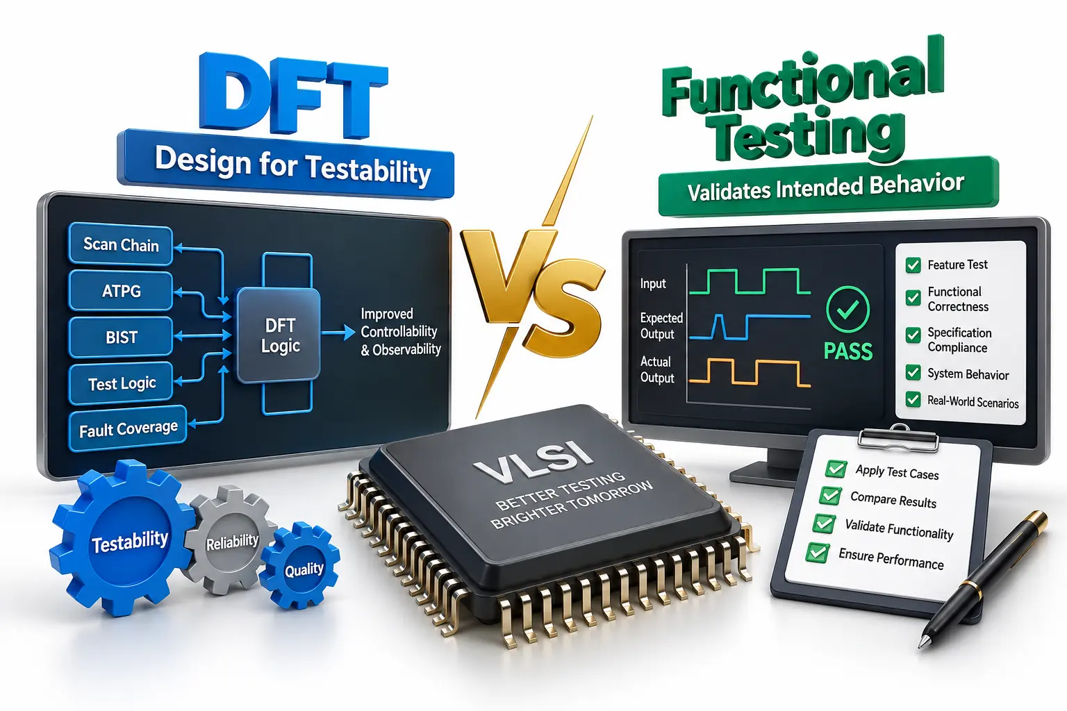
DFT vs Functional Testing in VLSI What's the Difference?
Navigate through this article using the table of contents below
Table of Contents
No headings found in this article.
A chip can correctly execute every function in its specification and still contain a manufacturing defect. That apparent contradiction explains why semiconductor companies cannot depend on functional testing alone when millions or billions of transistors must be tested after fabrication.
This is where Design for Testability changes the testing strategy. DFT and functional testing both contribute to chip quality, but they solve fundamentally different problems. Understanding that distinction is essential for anyone entering semiconductor design, verification, testing, or silicon validation.
Start With the Real Purpose of Testing a VLSI Chip
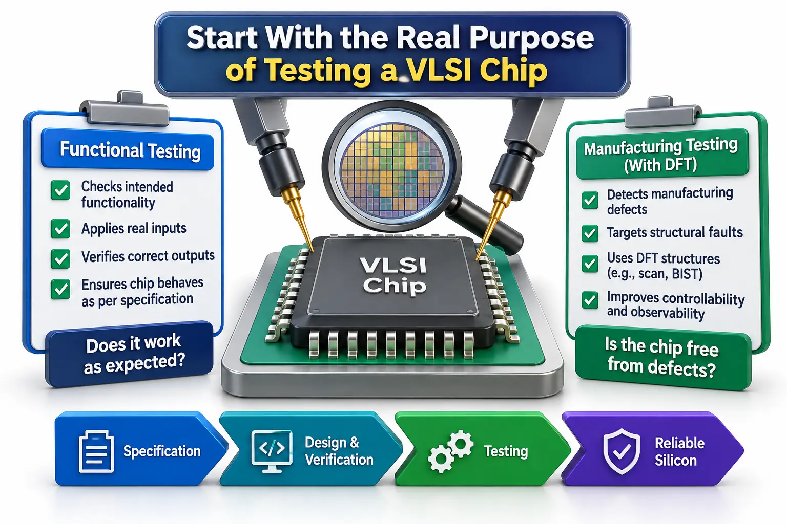
Before comparing DFT and functional testing, it is important to separate design correctness from manufacturing quality. During chip development, engineers verify whether the RTL and resulting implementation behave according to specification. After fabrication, however, the physical silicon may contain defects introduced during manufacturing.
Functional testing asks a behavior-oriented question: Does the chip perform the operations it was designed to perform? If a processor executes an addition instruction, for example, functional tests can provide operands and check whether the expected result appears.
Manufacturing-oriented testing asks a different question: Does the fabricated structure contain defects that could make the device unreliable or incorrect? Potential problems include:
Open interconnects
Shorts or bridging defects
Stuck-at behavior
Transition and timing-related faults
Memory defects
Defects affecting internal logic nodes
Testing every possible functional input and internal state of a modern SoC is impractical. Engineers therefore need structured techniques that make internal logic easier to control and observe.
Understand What DFT Actually Changes Inside the Design
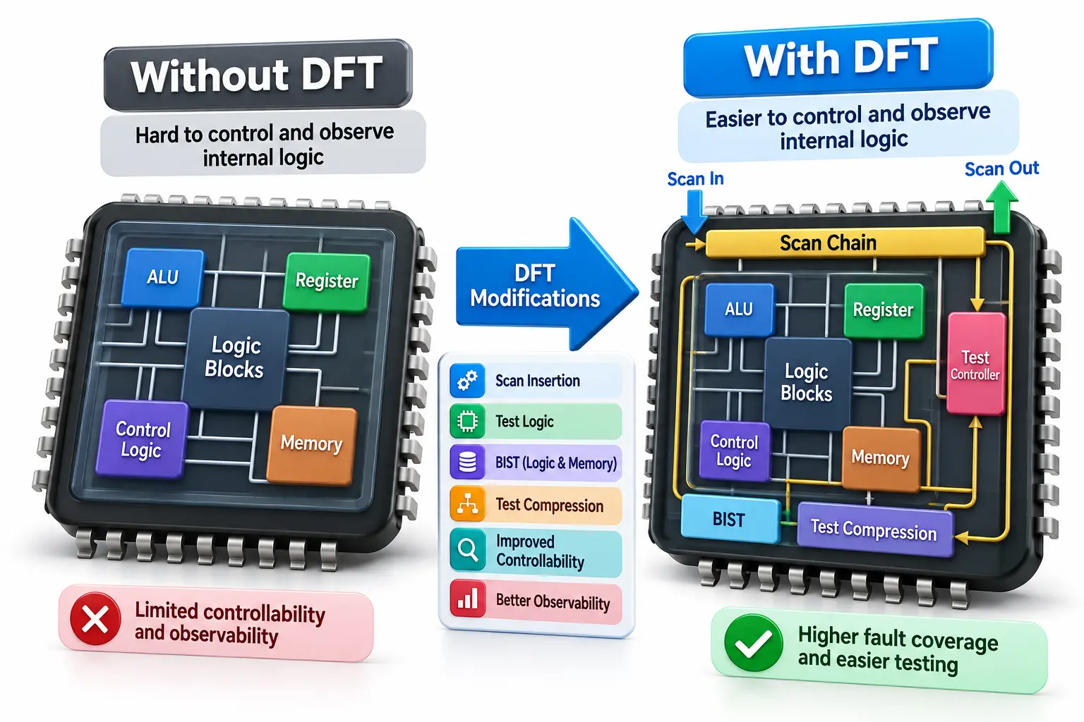
Design for Testability (DFT) is not simply a test executed after manufacturing. It is a collection of design techniques incorporated into the chip to make manufacturing defects easier to detect.
Consider a deeply buried flip-flop inside a large digital block. Through normal chip inputs and outputs, reaching a particular internal state and observing its response may require many clock cycles. DFT improves this controllability and observability by introducing dedicated test structures.
A typical DFT strategy can include:
Scan chains and scan-enabled flip-flops
Automatic Test Pattern Generation (ATPG)
Test compression
Logic Built-In Self-Test
Memory Built-In Self-Test
Boundary scan
Test controllers and dedicated test modes
With scan-based DFT, sequential elements can be connected into scan chains during test mode. Test data can be shifted into internal registers, a response can be captured, and results can be shifted out for evaluation.
For learners taking VLSI Training, this distinction is important because knowing digital design alone does not explain how a fabricated chip is screened for structural defects.
See How Functional Testing Approaches the Same Chip Differently
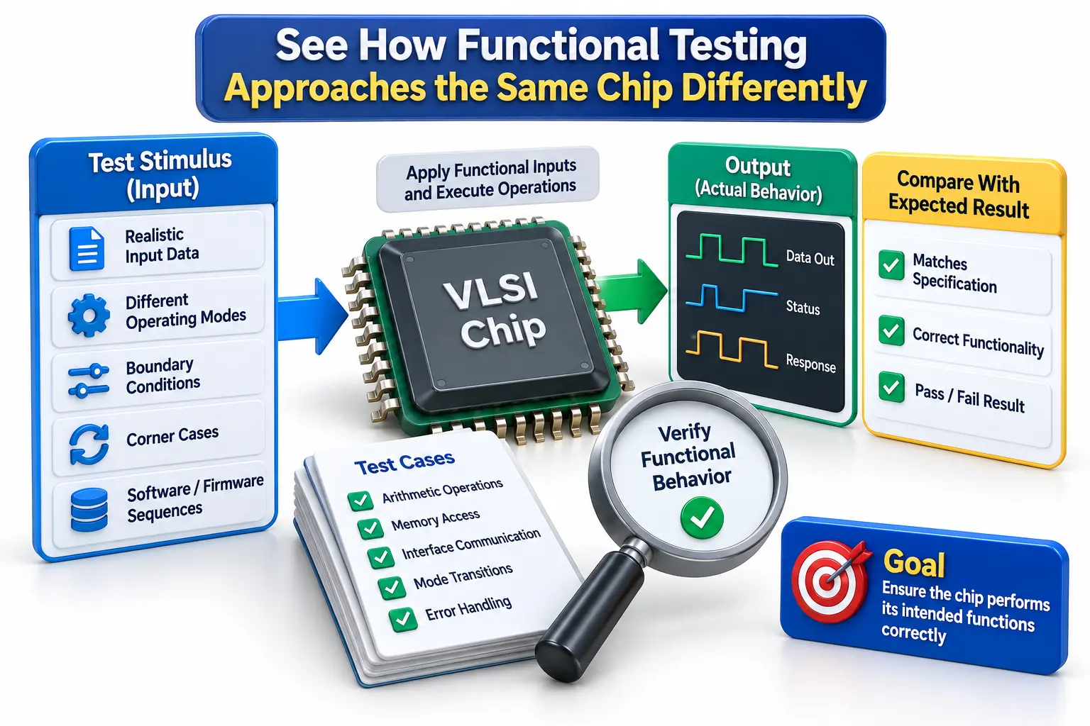
Functional testing concentrates on externally meaningful behavior. Instead of directly targeting an internal structural fault, engineers apply realistic operations and check whether the resulting behavior agrees with the specification.
Imagine a small arithmetic block supporting addition, subtraction, AND, and OR. Functional tests could apply different operands and operation codes, then compare actual outputs with expected results. Boundary values, unusual combinations, operating modes, and corner cases may also be included.
The fundamental approach looks like this:
Input stimulus → Execute intended function → Observe output → Compare against expected behavior
That sounds straightforward, but exhaustive functional testing quickly becomes unrealistic as complexity increases. A modern chip can contain enormous numbers of possible input sequences, states, software interactions, and operating conditions.
Functional testing is therefore valuable for demonstrating intended operation, but it does not automatically provide systematic coverage of physical defect models throughout the internal logic.
This is one reason students exploring DFT Training need to understand fault modeling and ATPG rather than treating DFT as another form of functional verification.
Compare Fault Models With Functional Scenarios
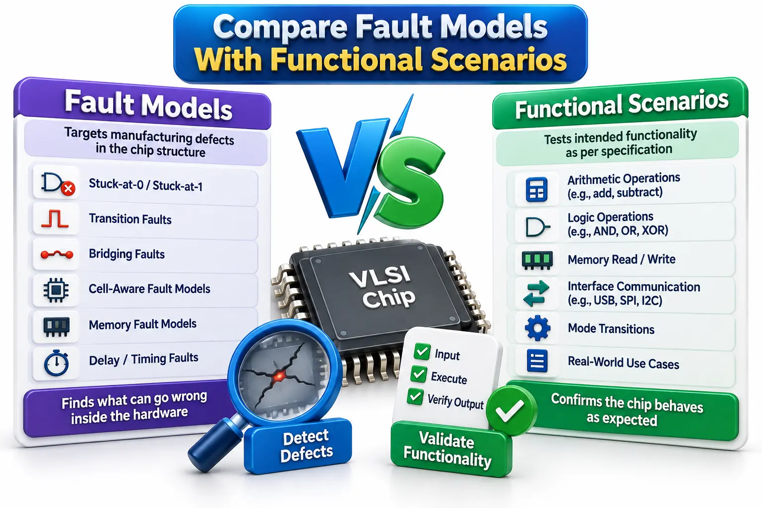
The clearest difference appears in how engineers decide what should be tested.
Functional testing begins with the specification and expected behavior. Engineers develop scenarios such as performing arithmetic, transferring data, executing instructions, accessing memory, or exercising communication interfaces. A test passes when observed behavior matches the expected result.
DFT-oriented structural testing begins with models representing possible physical defects. Instead of asking whether every useful operation works, ATPG attempts to create patterns capable of activating modeled faults and propagating their effects to observable points.
Common fault models include:
Stuck-at-0 and stuck-at-1 faults
Transition faults
Bridging-related faults
Cell-aware defect models
Memory-specific fault models
Suppose an internal node should switch between logic 0 and logic 1 but behaves as if permanently fixed at 0. A functional workload might accidentally expose the problem, but there is no guarantee that the necessary internal condition will occur.
An ATPG pattern is deliberately generated to activate the targeted modeled fault and make its effect observable. This targeted methodology is a major reason DFT is central to high-volume manufacturing test.
Follow What Happens From Design to Production Testing
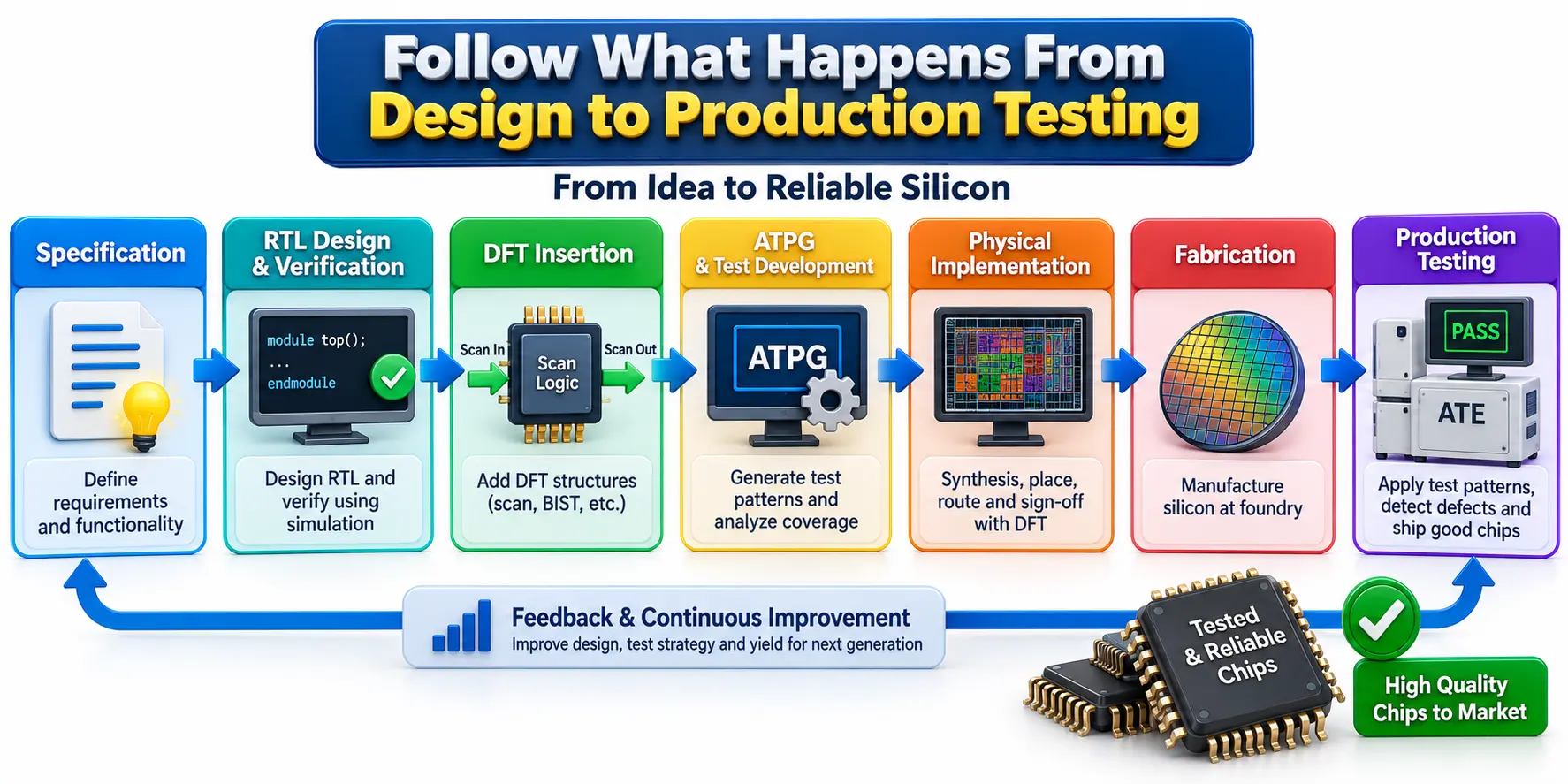
DFT and functional testing should not be viewed as competitors where engineers choose one and discard the other. They occupy different positions within a broader quality strategy.
During design development, functional verification checks whether RTL satisfies its specification. DFT structures are then integrated and validated so that they do not interfere with normal operation and can support the required manufacturing-test strategy.
A simplified journey looks like:
Specification → RTL design and verification → DFT insertion → ATPG → Physical implementation → Fabrication → Production test → System-level validation
After silicon arrives, automated test equipment can apply generated patterns to manufactured devices. Scan-based tests can target logic faults, while MBIST may address embedded memories. Other tests may cover interfaces, analog structures, performance, and electrical parameters.
Functional tests can then exercise meaningful chip capabilities that structural patterns are not intended to replace.
At JastTech, approaching the subject through this complete flow can help learners understand why semiconductor testing requires knowledge beyond simply writing test cases or running simulations.
Build the Right Skills for DFT and Functional Testing Careers
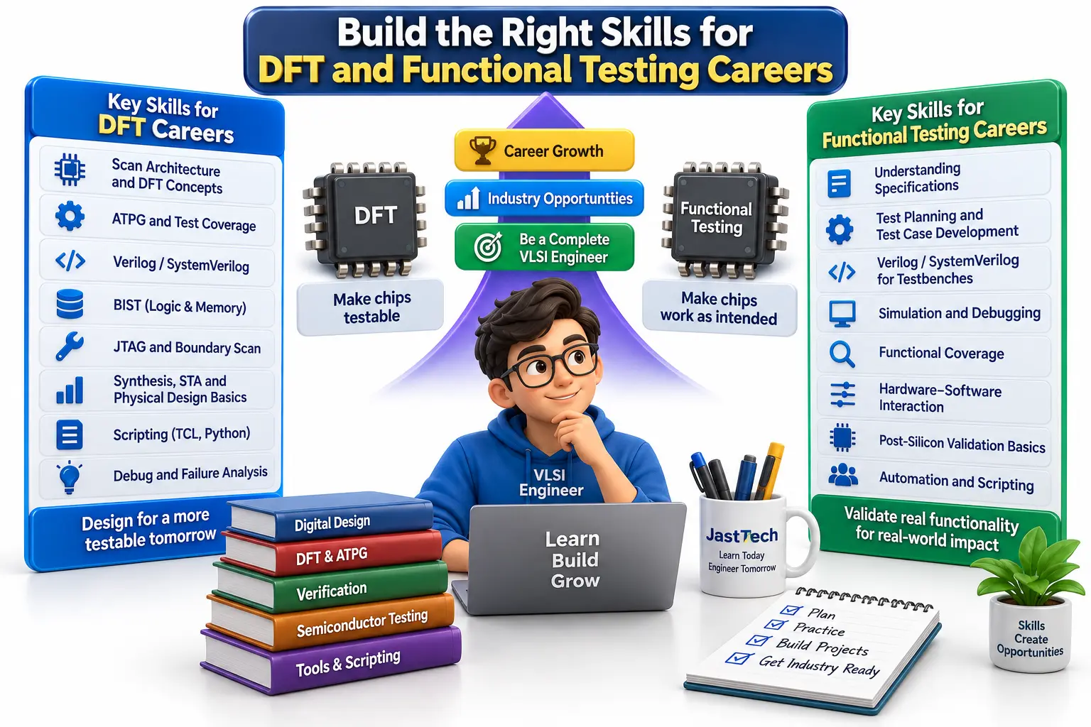
The career paths surrounding these activities also require different technical strengths. A DFT engineer works close to chip architecture, RTL, synthesis, scan infrastructure, ATPG, fault simulation, test coverage, timing constraints, and physical implementation.
Useful DFT skills include digital electronics, Verilog/SystemVerilog, scan architecture, ATPG concepts, fault models, compression, MBIST, JTAG, scripting, and familiarity with semiconductor design flows.
Functional testing roles can vary significantly depending on whether the work occurs during verification, emulation, post-silicon validation, production, or system testing. Engineers may need to understand specifications, interfaces, firmware, expected system behavior, debugging, test automation, and hardware/software interactions.
The simplest mental model is this:
Functional testing: Does the device perform its intended functions correctly?
DFT: Can the design be made controllable and observable enough for efficient manufacturing test?
Structural test: Can modeled defects in the fabricated structure be detected?
ATPG: Which patterns should be applied to detect targeted structural faults?
Functional verification: Did we design the intended logic correctly before fabrication?
Recognizing these boundaries prevents one of the most common mistakes beginners make: using “verification,” “functional testing,” “DFT,” and “chip testing” as though they describe exactly the same engineering activity.
Conclusion
DFT and functional testing ultimately contribute to the same objective—shipping dependable silicon—but they approach quality from different directions. Functional testing evaluates whether meaningful operations produce expected results, while DFT modifies the design so internal structures can be efficiently controlled, observed, and tested for manufacturing defects.
For aspiring VLSI engineers, understanding both creates a much clearer picture of the semiconductor lifecycle. Do not stop at definitions such as scan chain, ATPG, or test case. Learn why each technique exists, what problem it solves, and where it fits between RTL development and production silicon. That system-level understanding is what turns isolated concepts into practical engineering knowledge.