



Build a core engineering career with JastTech’s VLSI training institute in India. Master RTL & UVM with our top-tier VLSI course with placement support and 24/7 cloud EDA tool access.
Build a core engineering career with JastTech’s VLSI training institute in India. Master RTL & UVM with our top-tier VLSI course with placement support and 24/7 cloud EDA tool access.
Level
Advanced
Duration
6 Months
Trusted by Leading Organizations












JastTech is recognized as the best VLSI training institute in India, offering an advanced online learning ecosystem for aspiring semiconductor professionals. Our comprehensive curriculum bridges the hardware industry skill gap by delivering rigorous, hands-on tracks in architecture planning, physical design, and low-power DFT methodologies. Build a core engineering career with JastTech’s VLSI training institute in India. Master RTL & UVM with our top-tier VLSI course with placement support and 24/7 cloud EDA tool access.
Made for engineering graduates and working professionals nationwide, our specialized VLSI verification courses provide 24/7 cloud-based remote access to industry-standard EDA tools from Cadence and Synopsys. Learners are mentored directly by senior chip design veterans with over 10+ years of active silicon tape-out experience.
Backed by a network of 150+ global technology partners, this VLSI course with placement assistance helps our graduates start high-paying core engineering careers across top tech hubs. Secure your future in the growing semiconductor industry by joining India's leading training platform today.
JastTech is recognized as the best VLSI training institute in India, offering an advanced online learning ecosystem for aspiring semiconductor professionals. Our comprehensive curriculum bridges the hardware industry skill gap by delivering rigorous, hands-on tracks in architecture planning, physical design, and low-power DFT methodologies. Build a core engineering career with JastTech’s VLSI training institute in India. Master RTL & UVM with our top-tier VLSI course with placement support and 24/7 cloud EDA tool access.
Made for engineering graduates and working professionals nationwide, our specialized VLSI verification courses provide 24/7 cloud-based remote access to industry-standard EDA tools from Cadence and Synopsys. Learners are mentored directly by senior chip design veterans with over 10+ years of active silicon tape-out experience.
Backed by a network of 150+ global technology partners, this VLSI course with placement assistance helps our graduates start high-paying core engineering careers across top tech hubs. Secure your future in the growing semiconductor industry by joining India's leading training platform today.
Job Roles You Can Achieve
After completing this course
- VLSI Validation Engineer
- RTL Design Engineer
- DFT (Design for Testability) Engineer
- SoC Design Engineer
- Application Engineer (VLSI)
- STA (Static Timing Analysis) Engineer
- VLSI Validation Engineer
- RTL Design Engineer
- DFT (Design for Testability) Engineer
- SoC Design Engineer
- Application Engineer (VLSI)
- STA (Static Timing Analysis) Engineer
VLSI Training Institute in India Curriculum
Introduction to VLSI Technology
Learn semiconductor fundamentals, CMOS technology, and the complete VLSI design flow used in modern chip development.
Digital Electronics & Logic Design
Understand logic gates, Boolean algebra, combinational circuits, sequential circuits, FSMs, and digital design concepts.
Verilog HDL
Master Verilog HDL for modeling, designing, simulating, and testing digital circuits through practical RTL coding exercises.
SystemVerilog
Learn advanced verification concepts, assertions, randomization, OOP principles, and coverage-driven verification techniques.
RTL Design
Develop synthesizable RTL designs using industry-standard coding practices, optimization methods, and design techniques.
Related Courses
Training Roadmap
Seven intentional milestones — from first session to dream job.
Onboarding
- Meet your industry mentor
- Define your goals
- Skill gap assessment
Core Learning
- Live interactive classes
- AI-curated content
- Recorded sessions
Hands-on Practice
- Weekly assignments
- MCQ evaluations
- Module quizzes
Real Projects
- 3 live industry projects
- Portfolio building
- Case studies
Mentorship
- 1:1 doubt sessions
- Peer collaboration
- Expert feedback
Certification
- Exam preparation
- Practice dumps
- Industry-recognised certificate
Career Launch
- Resume crafting
- Mock interviews
- Job placement support
Practical Projects Built at Our VLSI Training in India
Skills and Tools You Will Learn
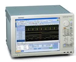
Logic Analyzers & Oscilloscopes
Verilog / System Verilog
RTL Coding
Testbench Writing
Lint & CDC
Synthesis
Waveform Debugging
Simulation
STA Basics
FPGA Prototyping
JTAG / OpenOCD
Oscilloscope tools
Lab View

Jenkins
Saleae Logic Analyzer
Verdi
Wireshark
Vivado
Python Basic
Available Course Schedules
Select a schedule that works best for you
Starts
26 Sept 2026
Time
09:30 AM – 12:30 PM
Duration
6 Months
Starts
28 Sept 2026
Time
07:00 AM – 09:00 AM
Duration
6 Months
Starts
03 Oct 2026
Time
02:00 PM – 05:00 PM
Duration
6 Months
Starts
05 Oct 2026
Time
08:00 PM – 10:00 PM
Duration
6 Months
Need a custom schedule?
Our team will craft the perfect batch for you.
What Our Happy Students Say
Real Feedback from our candidates
What We Offer Beyond Courses
24/7 Support
Round-the-clock assistance
LinkedIn Profile
Professional profile building
Resume Writing
Expert resume crafting
Alumni Guidance
Mentorship from graduates
Interview Prep
Mock interviews & tips
Live Projects
Real-world experience
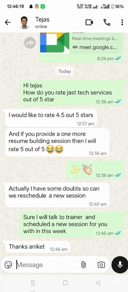
Tejas Kumar
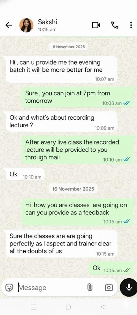
Sakshi Singh
Sanjay Patel
Specialized Training Programs
JastTech For Corporates
JastTech Courses
Why JastTech is Best VLSI Training Institute in India ?
See how we stand out from the competition
Designed by semiconductor engineers with modules covering RTL design, FPGA architectures, ASIC layouts, and verification methodologies.
Often relies on older academic syllabi that do not match modern semiconductor industry standards.
Students get 24/7 remote cloud access to licensed industrial EDA environments from Cadence and Synopsys for practical lab simulation.
Limited tool exposure, with an emphasis on theoretical presentation slides rather than active lab practice.
Learn directly from senior chip design veterans who have over 10 years of active tape-out experience in core companies
Taught by academic trainers who have limited or no exposure to real commercial silicon development.
Work on portfolio-worthy chip design and verification projects that strengthen technical and debugging capabilities.
Few opportunities to participate in structured, industry-inspired projects.
Weekly assignments, quizzes, and technical evaluations ensure continuous learning and concept clarity.
Assessments may be irregular and provide limited feedback for improvement.
Resume building, mock interviews, and placement guidance help students prepare confidently for VLSI job opportunities.
Career assistance and interview preparation may be minimal or unavailable.
Timely mentor support and one-on-one guidance ensure students receive help whenever required.
Slow response times and limited instructor availability can affect learning progress.
Earn a certification that validates practical VLSI knowledge and strengthens your professional profile.
Certificates may have limited recognition or practical value in the industry.
Get ongoing access to course recordings, study materials, and updated resources for continuous skill enhancement.
Learning resources may become unavailable after course completion or require extra payment.
A balanced fee structure with quality training makes JastTech a strong choice for learners comparing VLSI training institute in India fees and overall value.
Fees may be higher, with additional costs for resources, certifications, or extended access.
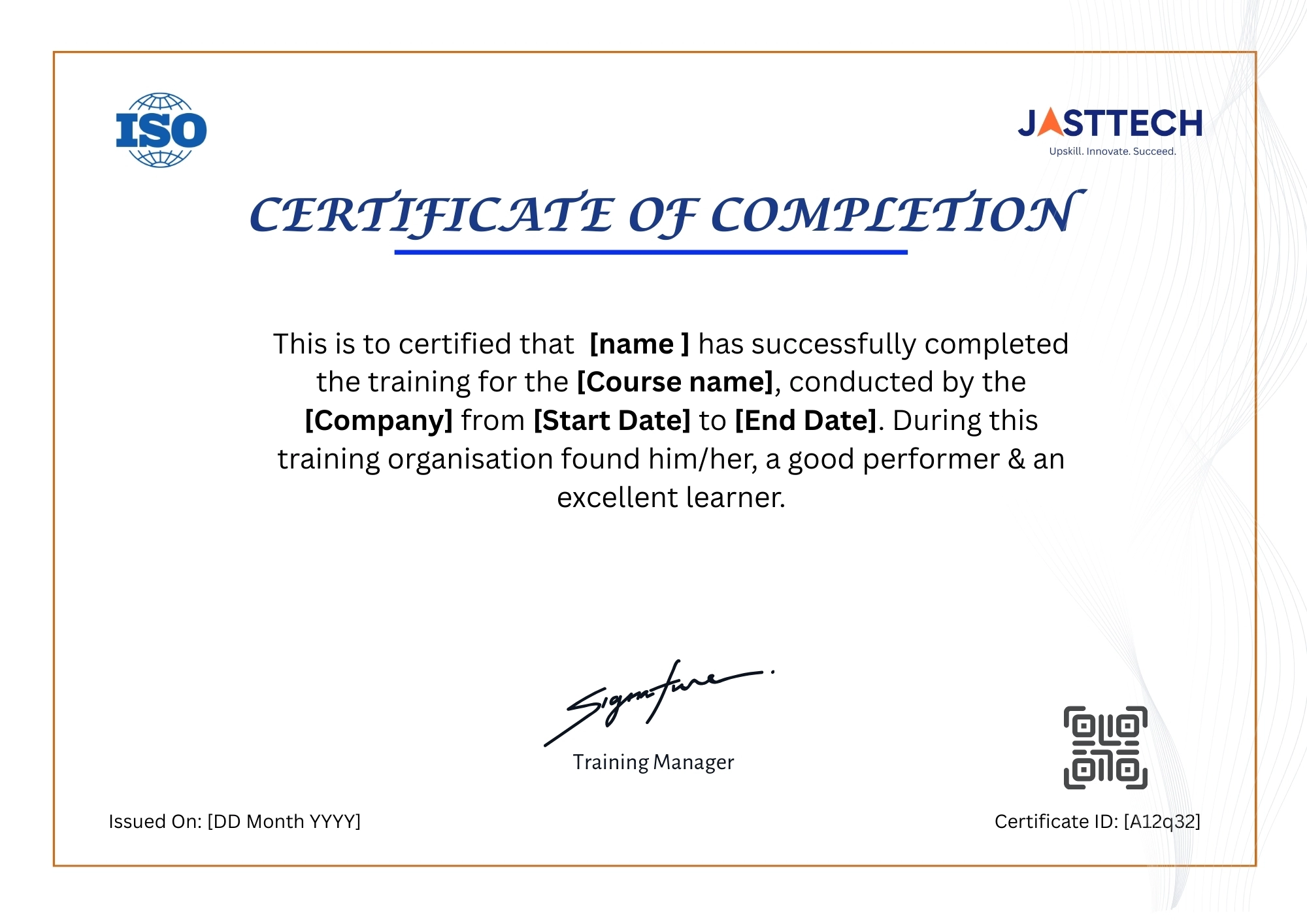
JastTech VLSI Training Institute Certificate
Prepare
Essential VLSI Technical Interview Questions
Curated questions with expert answers to help you ace your next interview.
What is the difference between Verilog and SystemVerilog?
Verilog is a hardware description language used for basic RTL modeling and simulation. SystemVerilog extends Verilog by introducing object-oriented programming, constrained randomization, and functional coverage, making it the global standard for advanced chip verification environments.
Explain Setup Time and Hold Time in sequential design
Setup time is the minimum duration a data signal must be stable before the active clock edge arrives. Hold time is the minimum duration it must remain stable after the clock edge passes. Violating either parameters causes data corruption due to metastability.
What is the difference between ASIC and FPGA architecture?
An ASIC is a custom-designed integrated circuit manufactured for a specific permanent application with optimized PPA. An FPGA is a standard programmable device containing configurable logic blocks that engineers can re-program multiple times post-fabrication.
Why do modern chip designers implement Design for Testability (DFT)?
DFT introduces specialized test structures like scan chains, BIST, and boundary scan into the circuit layout. This allows manufacturing plants to rapidly catch physical silicon defects using automated test patterns (ATPG) before shipping chips to clients
What is metastability and when does it typically occur in VLSI?
Metastability is an unstable hardware state where a flip-flop output fails to settle into a stable 0 or 1 within the required time. It typically occurs at clock domain crossings (CDC) or when setup and hold timing windows are violated during data transfers.
Support
Everything You Need to Know About Our VLSI Course
Can't find what you're looking for? Reach out to our support team anytime.
What should I look for when choosing a VLSI training institute in India?
A reliable VLSI Training Institute center must offer hands-on lab practice alongside theory. At JastTech, we support our students with 24/7 remote cloud access to industrial EDA tools so you can run simulations from home anytime.
Why do engineering graduates consider JastTech the best VLSI training institute in India?
Most colleges teach chip design from old textbooks, which leaves students unprepared for actual job roles. We focus entirely on current industry workflows, teaching everything from basic RTL coding to advanced silicon tape-out methodologies.
Does JastTech provide a VLSI course with placement assistance?
Yes, our training includes dedicated placement support. Our team helps you prepare for technical rounds through mock interviews and resume building, before introducing you to our network of over 150 hiring partners.
How does this program compare to separate VLSI verification courses?
You do not need to buy a separate course for validation. Our regular curriculum includes deep-dive modules on system-level testing, giving you the same depth as specialized verification tracks covering SystemVerilog, UVM, and testbench setups.
Do students get to work on real semiconductor tools?
Yes. You will get individual cloud access to license-based EDA environments from Synopsys and Cadence. Learning on these exact platforms is critical because they are the standard tools used by top core companies.
The support team was very cooperative and responsive. They made sure all doubts were cleared without delay. Great experience overall.
I had a great experience with the RF Circuit Design course. Thanks to the teaching staff for such a well planned and structured curriculum it really helped me clear my technical certification for my job.
I enrolled in the Post-Silicon Validation Certification Training at JastTech and found it quite different from typical courses. They focus on debugging techniques and real chip-level scenarios, which gave me a better idea of how things work.
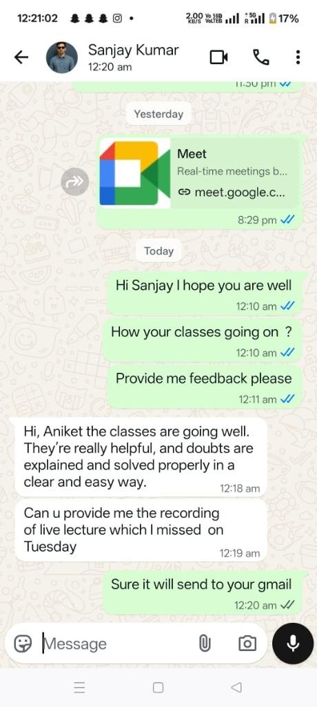
One thing I really liked about the Data Analyst course at JastTech is their focus on consistency. Regular sessions and tasks help you stay on track and build a daily learning habit. Also, they provide recordings after live sessions, which help in revision.
I joined JastTech for the DFT course a few months back. At first, I wasn’t sure what to expect, but the classes turned out to be really helpful. The teaching is simple and not too complicated, which helped me keep up.
Take the Next Step in Your Career
Join thousands of learners who have upgraded their skills with our industry-focused training programs. Our experts are here to guide you every step of the way.
Related Articles & Insights
Deep dive into VLSI Training Institute in India with our expert-curated technical guides and industry updates.
Complete Guide to ServiceNow GRC/IRM & AI Governance for Beginners

Common Mistakes Freshers Make While Learning Embedded Systems and How to Avoid Them

What Is the Difference Between a Latch and a Flip-Flop in VLSI?
Confused about latches and flip-flops in VLSI? Discover how level-sensitive and edge-triggered storage differ, why unintended latches appear in RTL, and how both affect timing, synthesis, and real chip design.

Which Guidewire Module Should You Learn First in Bangalore? ClaimCenter vs PolicyCenter vs BillingCenter
Confused about which Guidewire module to start with? Here's a practical, Bangalore-focused breakdown of ClaimCenter, PolicyCenter, and BillingCenter to help you choose the right one first.
We're Here to Help –
Reach Our Global Offices
Hyderabad
JastTech
Training & Development Center
91 Springboard Business Hub ,Madhapur LVS Arcade, 71, Jubilee Enclave, HITEC City, Hyderabad,India Telangana 500081
Pune
JastTech
Training & Development Center
Sr. No. 30/2/1, 3rd Floor, Above Rajrshi Shahu Bank & BOB Balaji Nagar, Dhankawadi, Katraj, Pune, Maharashtra 411043
Noida
JastTech
Training & Development Center
B 8, B Block, Sector 2, Noida, Metro Station Rd, near sector 15 Metro, Uttar Pradesh 201301
Hyderabad
JastTech
Training & Development Center
91 Springboard Business Hub ,Madhapur LVS Arcade, 71, Jubilee Enclave, HITEC City, Hyderabad,India Telangana 500081
Pune
JastTech
Training & Development Center
Sr. No. 30/2/1, 3rd Floor, Above Rajrshi Shahu Bank & BOB Balaji Nagar, Dhankawadi, Katraj, Pune, Maharashtra 411043
Noida
JastTech
Training & Development Center
B 8, B Block, Sector 2, Noida, Metro Station Rd, near sector 15 Metro, Uttar Pradesh 201301
Can't find a JastTech location near you? Contact us for more information.