

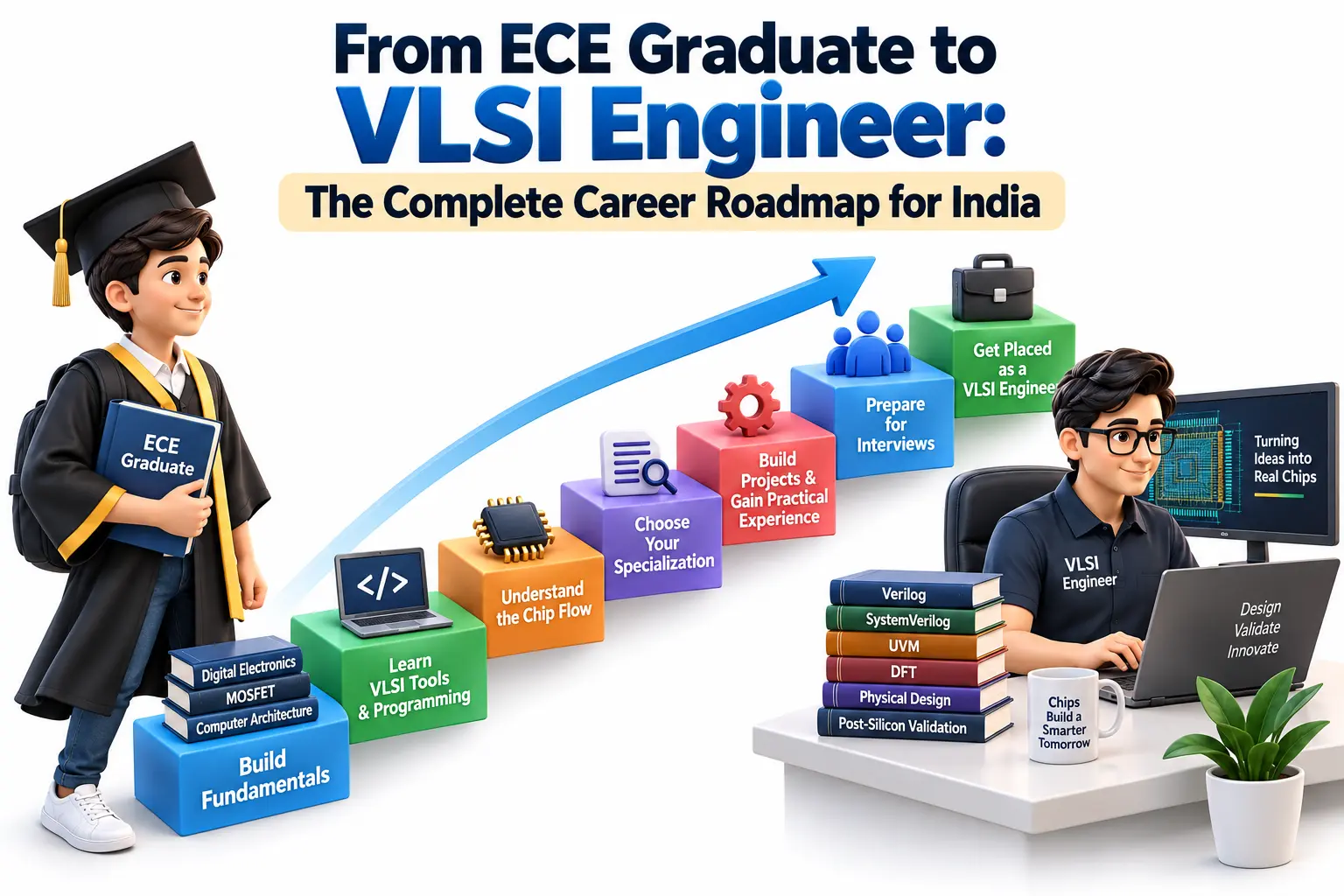
From ECE Graduate to VLSI Engineer: The Complete Career Roadmap for India
Navigate through this article using the table of contents below
Table of Contents
No headings found in this article.
An ECE degree gives you the foundation for semiconductor engineering—but it does not automatically make you ready for a VLSI job. Between college electronics and an actual chip-design role lies a skill gap involving RTL, verification, timing, EDA tools, debugging, scripting, and practical projects.
The good news is that you do not need to master the entire semiconductor industry. You need the right sequence. By strengthening fundamentals, understanding the chip flow, choosing one specialization, building evidence of your skills, and preparing strategically, you can turn your ECE background into a focused VLSI career.
Build the Electronics Foundation That VLSI Interviews Actually Test
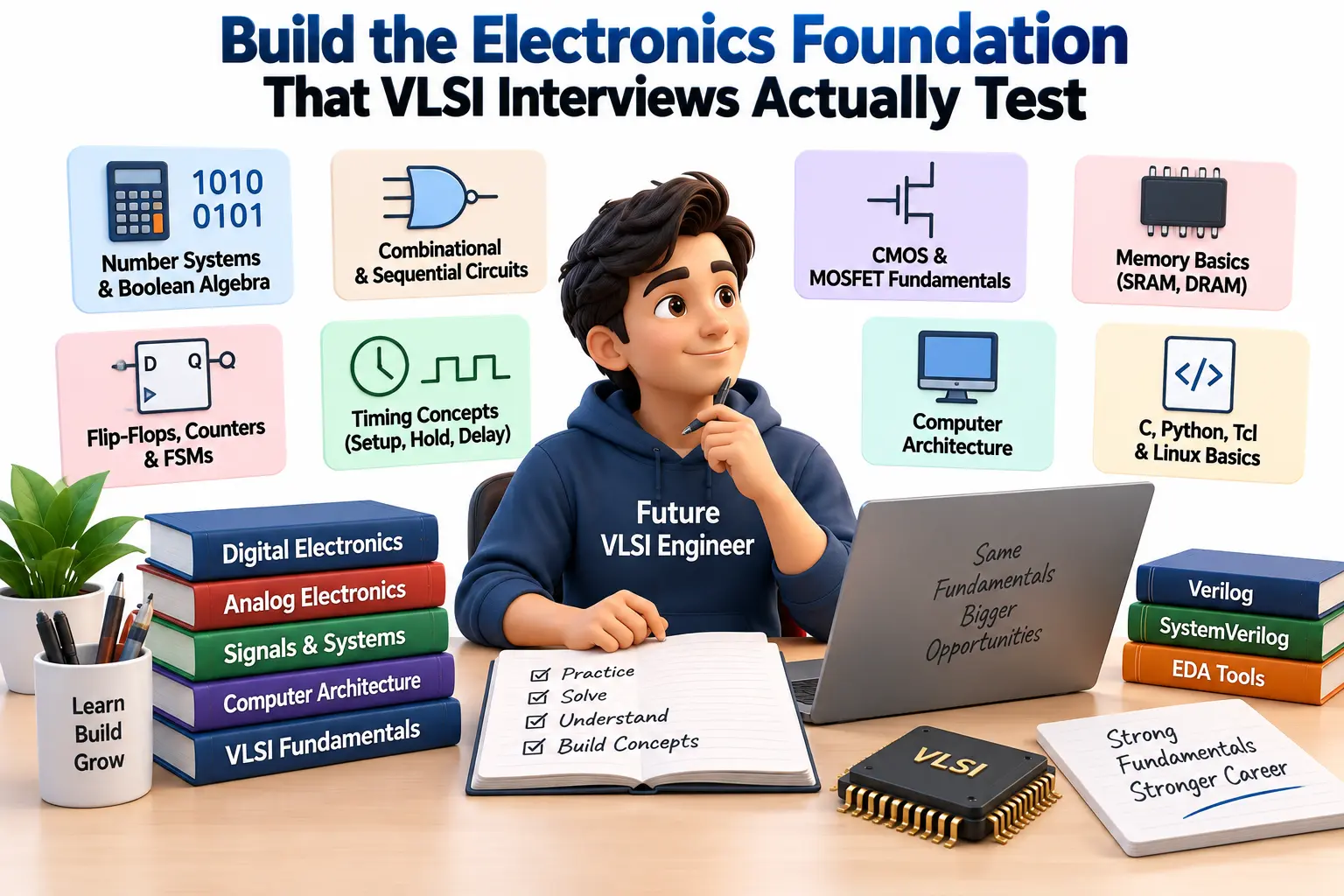
Many ECE graduates make their first mistake by immediately learning advanced SystemVerilog, UVM, physical design tools, or other specialized technologies. VLSI sits on top of digital electronics and semiconductor fundamentals. If those fundamentals are weak, advanced training becomes memorization instead of engineering.
Start by rebuilding the concepts that repeatedly appear in VLSI work and interviews:
Number systems and Boolean algebra
Combinational and sequential circuits
Flip-flops, counters, registers and FSMs
Setup time, hold time and propagation delay
Clocking and synchronization concepts
CMOS and MOSFET fundamentals
Memory basics
Computer architecture fundamentals
Do not study these only as definitions. Ask engineering questions. Why does a setup violation occur? What happens when an asynchronous signal enters a synchronous circuit? How would you design an FSM for a protocol controller? Why are flip-flops needed? The ability to reason through such questions separates an interview-ready candidate from someone who has simply completed a course.
Programming should develop alongside electronics. C helps you understand low-level systems, while Python, Tcl or shell scripting becomes valuable for automation, data processing and EDA workflows. Linux command-line familiarity is also important because semiconductor engineering environments frequently depend on Linux-based workflows.
Understand the Complete Chip Flow Before Choosing Your Specialization
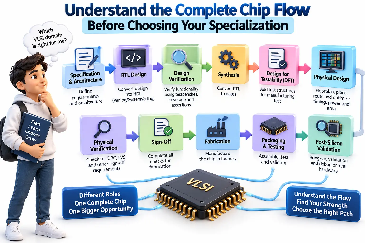
VLSI is not a single job. A chip moves through several engineering stages, and different teams own different parts of that journey. Before choosing a career path, understand the basic sequence from specification and architecture through RTL, verification, synthesis, DFT, physical implementation, sign-off, fabrication and silicon validation.
This perspective prevents a common fresher mistake: learning a tool without understanding where it belongs. For example, RTL engineers describe digital hardware, verification engineers prove that the design behaves correctly, DFT engineers improve testability, and physical design engineers transform the logical implementation toward manufacturable silicon.
Common career directions include:
RTL Design
Design Verification
Physical Design
Design for Testability
Static Timing Analysis
Analog and Mixed-Signal Design
FPGA Design
Physical Verification
Post-Silicon Validation
Product and Test Engineering
Spend enough time understanding these roles to identify what matches your strengths. Someone who enjoys logic design may prefer RTL. A student who loves debugging and finding corner cases may fit verification. Engineers interested in timing, optimization and implementation may prefer physical design, while candidates who enjoy hardware-software interaction can explore validation.
Choose One VLSI Domain and Build Depth Instead of Learning Everything
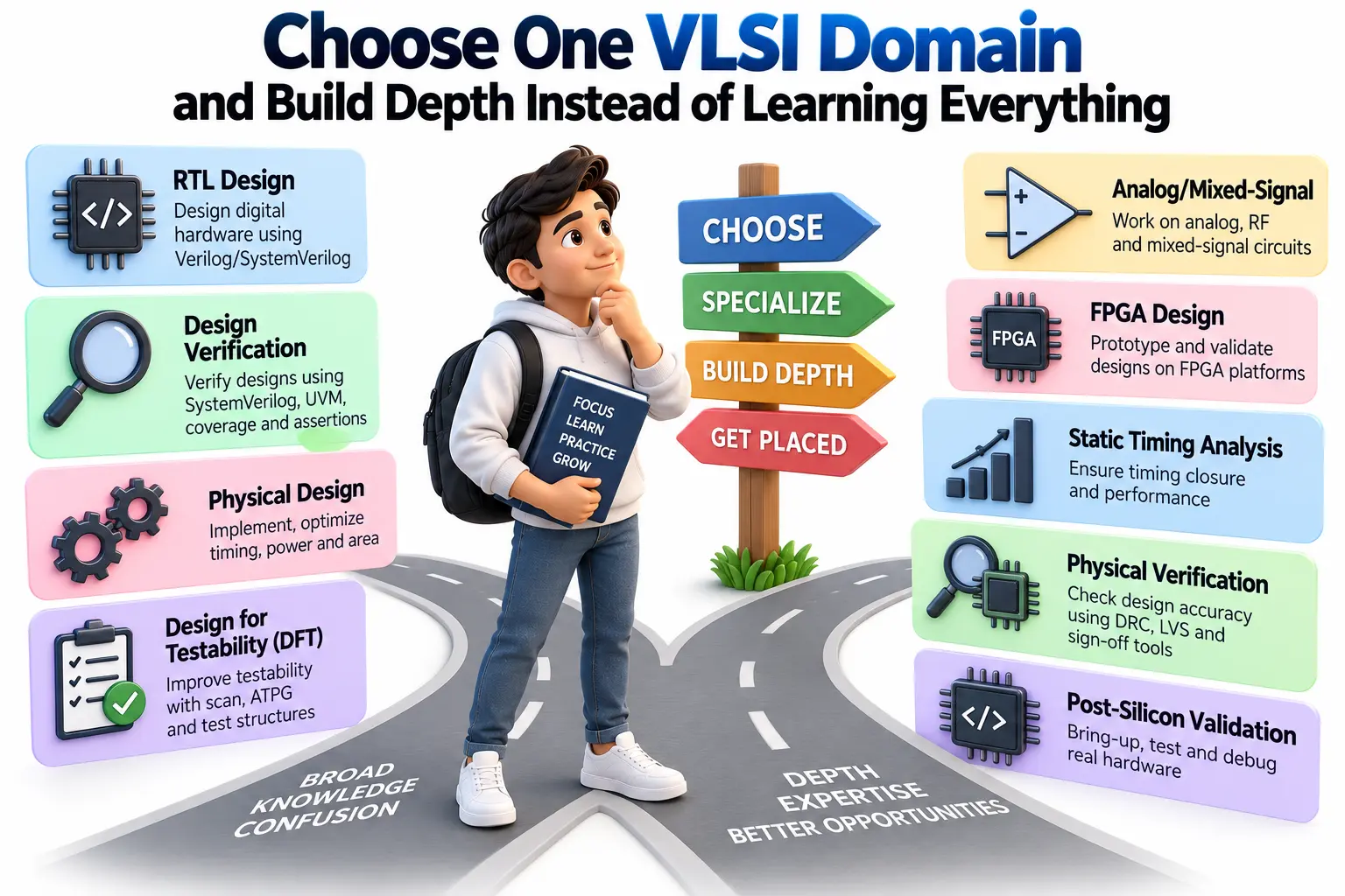
Once you understand the ecosystem, specialization becomes critical. Trying to simultaneously master RTL, UVM, DFT, physical design, analog design and validation usually creates a broad but shallow profile. Recruiters hire candidates for specific requirements, so your resume should communicate a clear technical direction.
For an RTL path, concentrate on Verilog/SystemVerilog, synthesizable coding, FSM design, pipelining, clock/reset strategies, synthesis awareness and timing fundamentals. Verification candidates should develop SystemVerilog, assertions, constrained random verification, functional coverage, UVM concepts, debugging and protocol knowledge.
Physical design candidates need a different stack: synthesis awareness, floorplanning, placement, clock tree synthesis, routing, timing closure, congestion, power considerations and sign-off concepts. DFT aspirants should understand scan architecture, ATPG, fault models, test coverage and memory test concepts.
Training can accelerate this process when it provides structured labs, mentorship and project feedback. When evaluating a vlsi training institute in India, focus less on the number of tools listed in the syllabus and more on whether students actually solve design, verification and debugging problems independently.
JastTech can be considered by students looking for structured learning that connects semiconductor concepts with practical, role-oriented preparation. The important objective of any training path should be simple: convert theoretical knowledge into skills you can demonstrate during a technical interview.
Turn Projects Into Proof That You Can Think Like an Engineer
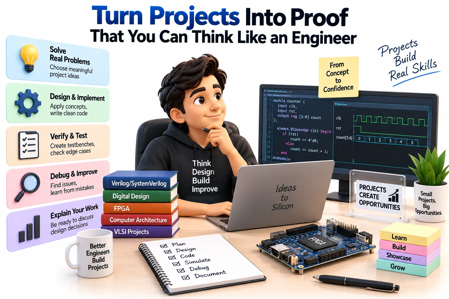
Projects should be the bridge between learning and employment. Unfortunately, many freshers treat projects as resume decoration. Writing “UART Design using Verilog” means little if you cannot explain the architecture, state transitions, test strategy, bugs encountered and design decisions.
Build projects in increasing complexity. Begin with counters, FIFOs, arbiters and FSM-based controllers. Then move toward UART, SPI, I2C, memory controllers or simplified protocol-based designs. Your final projects should match the role you are targeting rather than being random electronics projects.
For every serious project, be prepared to explain:
What problem were you solving?
Why did you choose that architecture?
How did you verify the design?
Which corner cases did you test?
What bugs appeared?
How did you debug them?
What would you improve in the next version?
Verification candidates should show testbench architecture, assertions, coverage and failure analysis. RTL candidates should demonstrate clean synthesizable design and timing awareness. Physical design candidates should understand implementation results rather than merely displaying tool screenshots.
Students interested in silicon bring-up, board-level debugging, firmware interaction, registers and hardware validation can also explore Post Silicon Validation Training in India as a specialized route into semiconductor validation. This path particularly suits ECE graduates who enjoy combining electronics, C programming, interfaces, instruments and systematic debugging.
Prepare for VLSI Interviews as Engineering Problems, Not an Exam
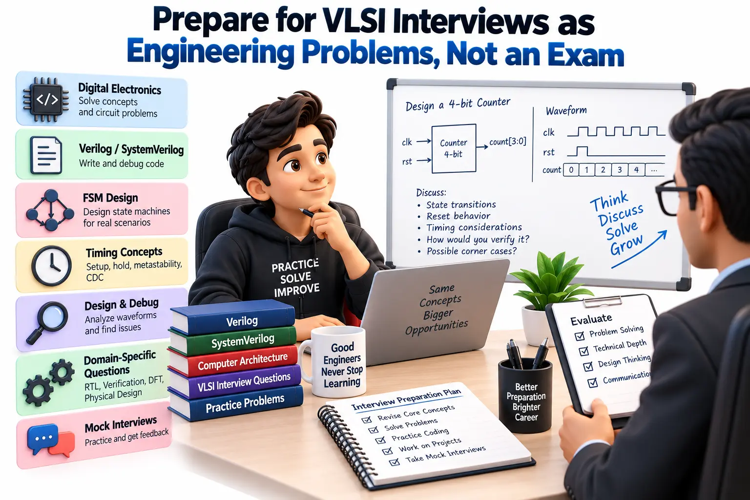
VLSI interviews often expose the difference between memorized knowledge and real understanding. An interviewer can begin with a simple flip-flop question and gradually move into setup/hold timing, metastability, clock-domain crossing or an RTL design problem. Preparing only a list of definitions therefore creates false confidence.
Practice concepts by drawing circuits, writing RTL without copying templates, predicting waveforms and explaining your reasoning aloud. For every important topic, prepare at three levels: definition, application and debugging.
A strong preparation cycle includes:
Digital electronics problem solving
Verilog/SystemVerilog coding
Timing questions
FSM design
Basic computer architecture
Domain-specific technical questions
Project explanation
Debugging scenarios
Aptitude and logical reasoning
Mock technical interviews
Your project should become one of your strongest interview assets. Interviewers may ask why you selected a particular architecture, how you verified it or what happened when something failed. Candidates who can discuss mistakes and debugging decisions often demonstrate more engineering maturity than candidates presenting a supposedly perfect project.
Build a Job-Search System That Targets Semiconductor Roles Strategically
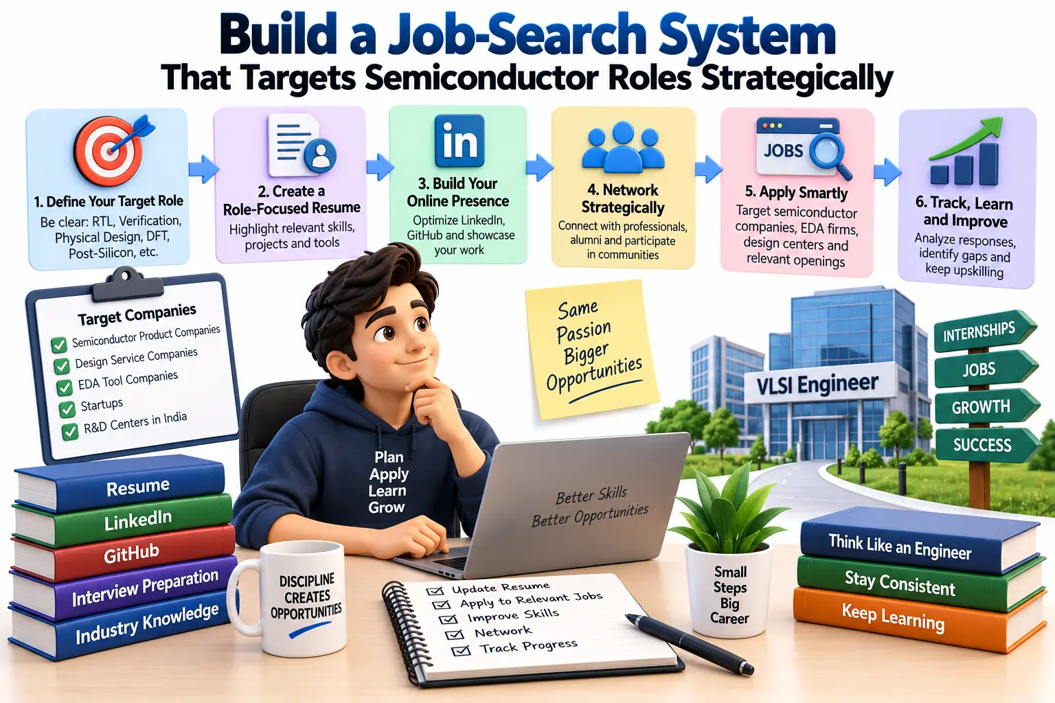
Becoming technically ready is only part of the roadmap. Your job-search strategy must communicate that readiness. Instead of creating a generic ECE resume and applying to hundreds of unrelated positions, create a role-focused profile.
If your target is design verification, your resume headline, skills and projects should consistently support verification. The same principle applies to RTL, DFT, physical design or validation. Put your strongest relevant projects near the top and describe what you actually designed, verified, automated or debugged.
Build visibility through LinkedIn, GitHub, alumni connections, technical communities, internships, referrals and semiconductor hiring platforms. Follow semiconductor companies, engineering service organizations, EDA companies, startups and design centres operating across Bengaluru, Hyderabad, Pune, Chennai, Noida and other Indian technology hubs.
Most importantly, treat rejection as technical feedback. Track the questions you could not answer, concepts where you struggled and roles where your profile received responses. Improve those areas and repeat the cycle. A focused candidate who continuously measures weaknesses can progress faster than someone endlessly collecting certificates.
Conclusion
The transition from ECE graduate to VLSI engineer is not about learning every semiconductor technology available. It is about building skills in the correct order: strengthen electronics fundamentals, understand the chip-development flow, select one specialization, develop practical projects, master debugging and prepare specifically for technical interviews.
India's semiconductor ecosystem gives electronics graduates multiple directions, but opportunity alone will not make a candidate industry-ready. Build depth instead of collecting disconnected skills. With focused learning, practical engineering work and a disciplined application strategy, your ECE degree can become the starting point for a long-term career in chip design, verification, implementation or silicon validation.