

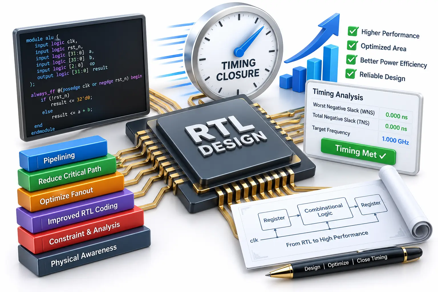
High-Speed RTL Design: Timing Closure Techniques Every Engineer Should Know
Navigate through this article using the table of contents below
Table of Contents
No headings found in this article.
A design can be functionally perfect and still fail as silicon. When clock frequency rises, a few picoseconds hidden inside combinational logic, routing, fanout, or an innocent-looking multiplexer can turn clean RTL into a timing-closure problem that survives every optimization attempt.
That is why high-speed RTL design is not simply about writing compact Verilog. Engineers must think about the hardware that synthesis will create, the paths physical design must route, and the amount of work that must fit between consecutive clock edges. Timing closure starts much earlier than sign-off.
Start Timing Closure at the RTL Architecture, Not at the Timing Report
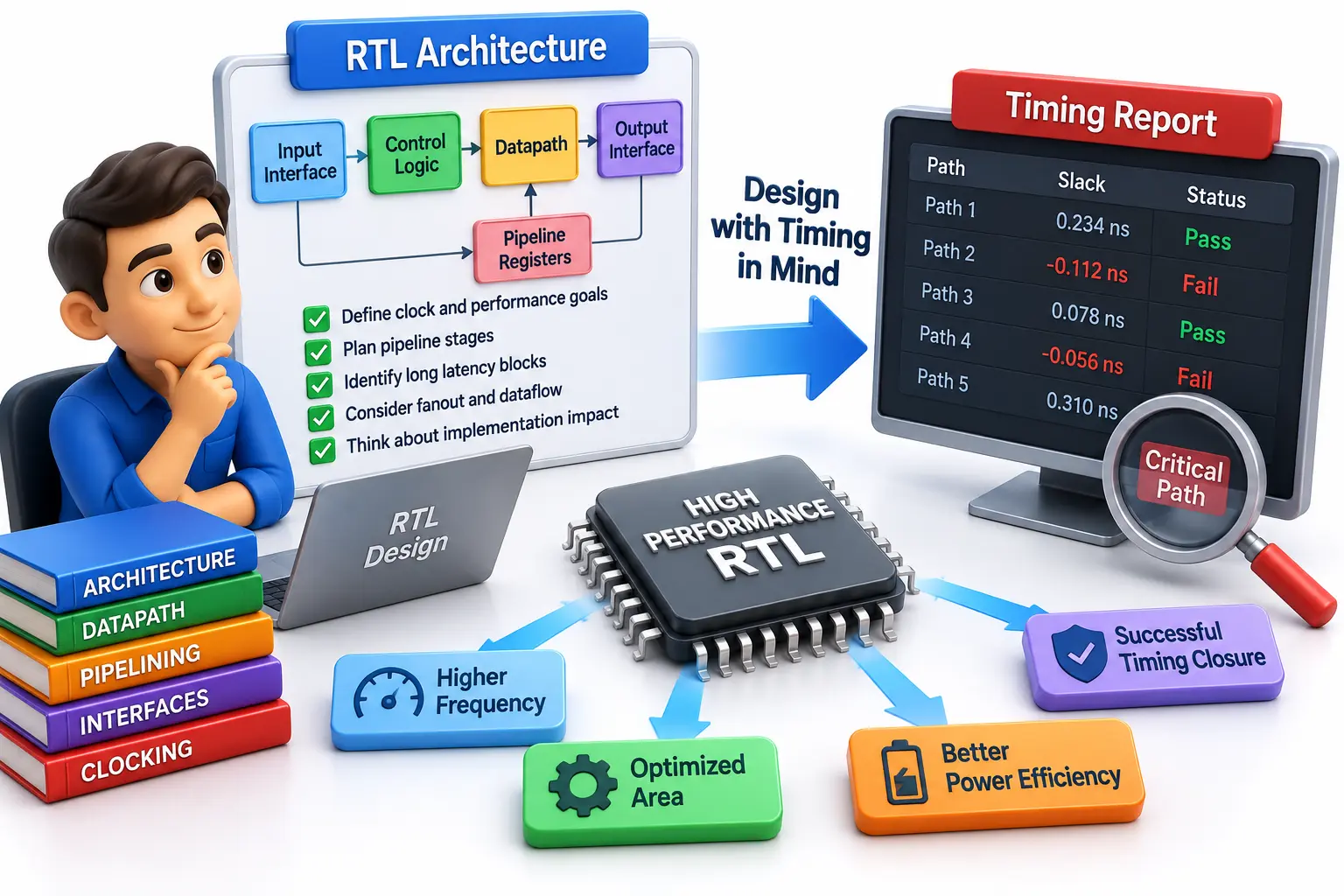
Timing closure means ensuring that data reaches its destination within the timing requirements imposed by the design. For a synchronous data path, the basic journey is straightforward: a launch flip-flop sends data through combinational logic and routing before a capture flip-flop samples it.
As clock frequency increases, the available period becomes smaller. A 500 MHz clock provides only 2 ns per cycle before accounting for clock uncertainty, setup requirements and other margins. RTL that comfortably operates at 100 MHz can therefore become impossible at a much higher target frequency.
Before writing a complex block, engineers should identify:
Target clock frequency and clock period
Long arithmetic operations
Deep decision and priority logic
Large multiplexers
Wide comparisons and reductions
High-fanout control signals
Cross-module paths
Expected pipeline boundaries
This is where high-speed architecture begins. If one cycle contains address calculation, comparison, selection and arithmetic before storing the result, synthesis cannot magically eliminate the fundamental amount of work.
JastTech encourages learners to develop this architecture-first mindset because timing problems are easier to prevent during RTL development than to repair after an entire subsystem has been integrated.
Break Critical Paths With Intelligent Pipelining
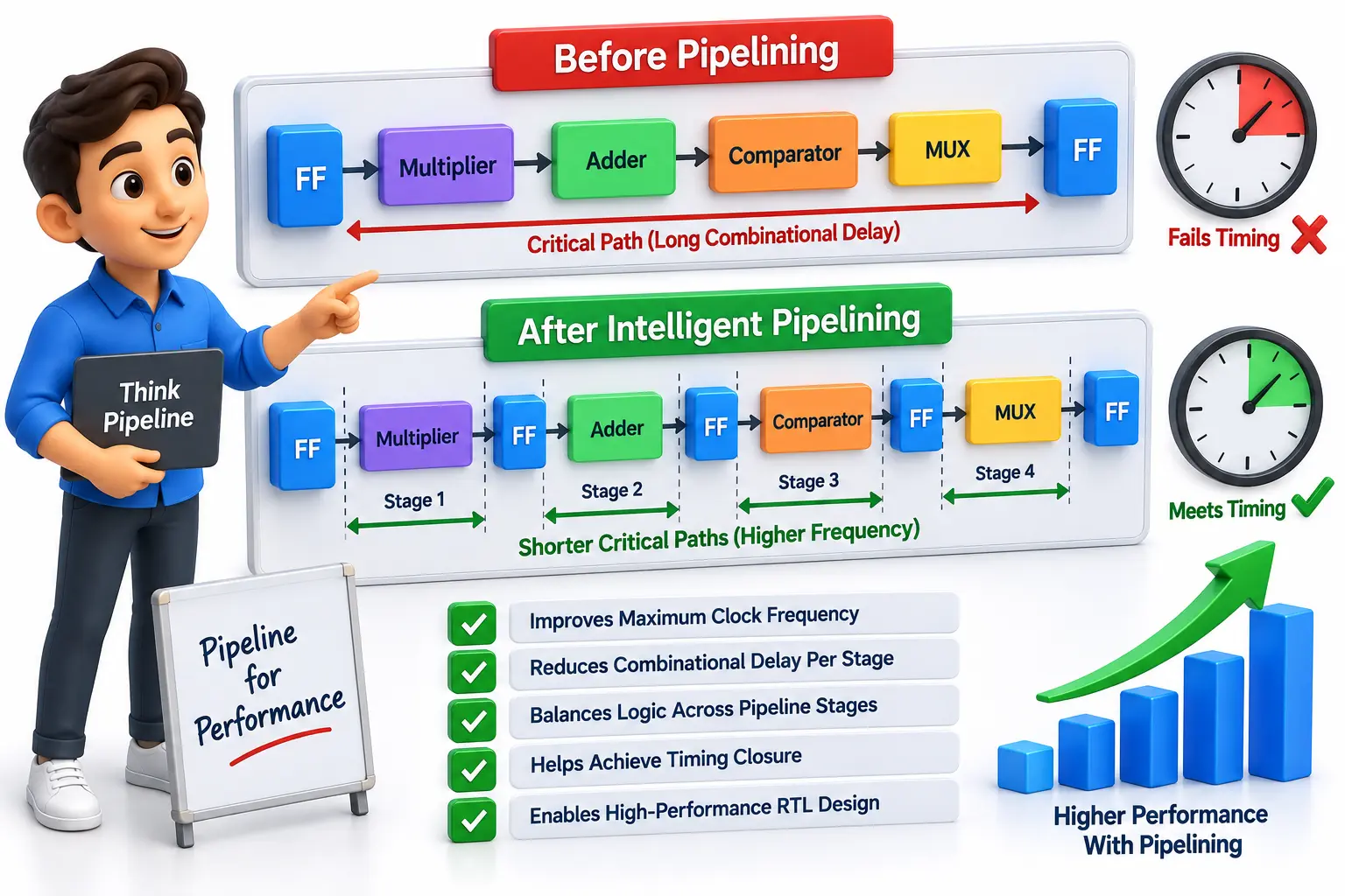
Pipelining is one of the most powerful techniques for increasing achievable clock frequency. Instead of forcing a large combinational operation to complete within one clock cycle, registers divide the operation into smaller stages.
Imagine a datapath performing multiplication, addition, comparison and output selection in a single cycle. Even if each operation is individually reasonable, their combined propagation delay may exceed the available clock period. Adding pipeline registers can distribute that work across multiple cycles.
For example, the architecture can become:
Stage A — capture and preprocess inputs
Stage B — perform arithmetic
Stage C — comparison and selection
Stage D — register the final result
The important word is intelligent. Adding registers everywhere increases latency, area, clock-tree load and verification complexity. The goal is balanced pipeline stages where no individual stage contains disproportionately more logic than the others.
Pipeline planning also affects control signals. Valid, enable, transaction ID and other metadata must remain aligned with corresponding data. Engineers therefore need to optimize performance without changing functional transaction behavior.
Anyone taking RTL Design and Verification Training in India should practice pipelining using real datapaths rather than treating it as a definition. Timing-aware RTL becomes much easier once engineers can look at an expression and mentally estimate the hardware stages it may require.
Reduce Combinational Depth Before It Becomes a Critical Path
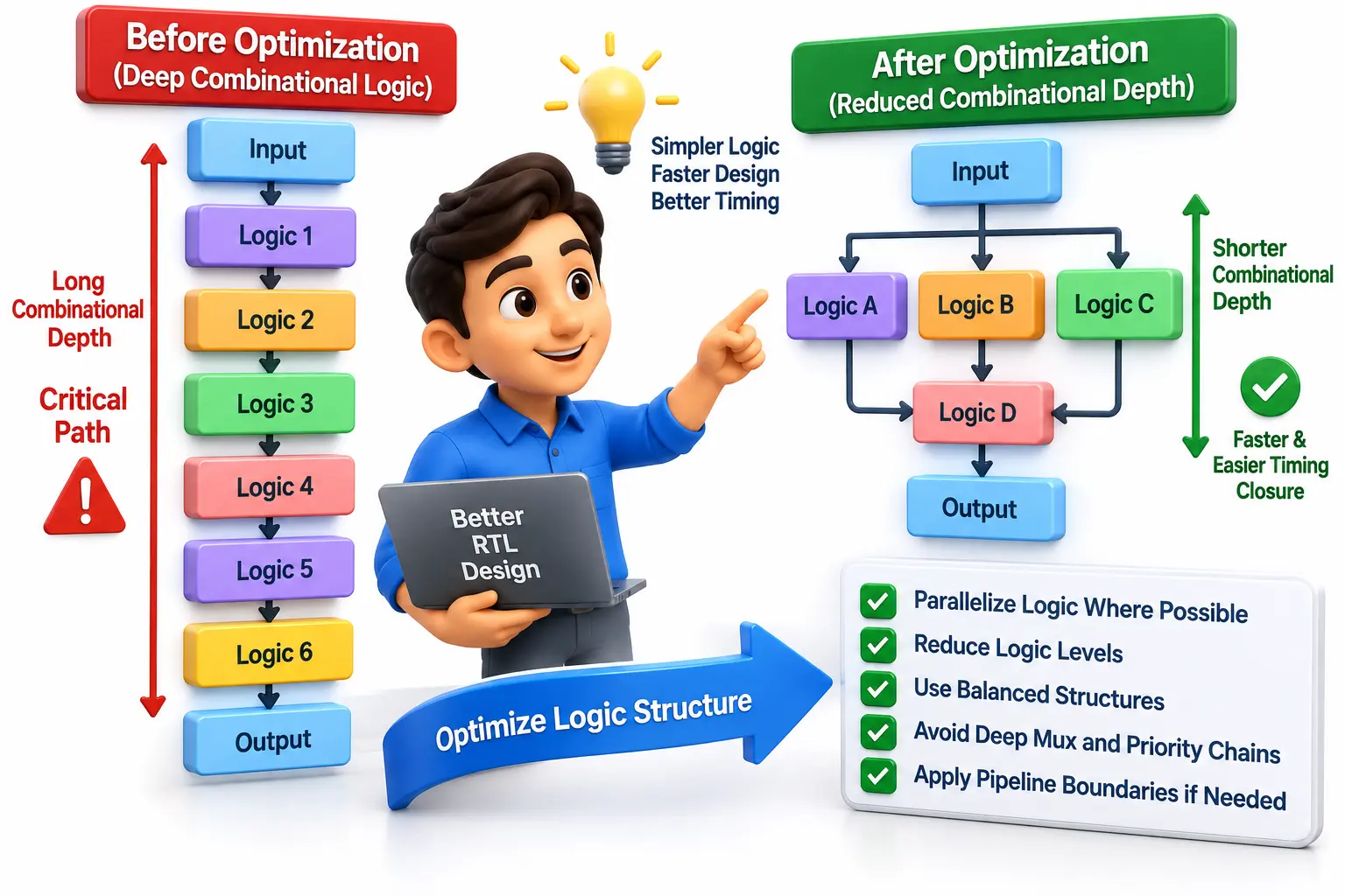
RTL can appear short while synthesizing into deep hardware. A nested conditional statement, long priority chain or complicated expression can create multiple levels of multiplexers and logic gates between two registers.
Consider a large priority structure. If many conditions are evaluated sequentially, the synthesized circuit may contain a long selection chain. At high frequencies, this structure can become the critical path even though the RTL itself occupies only a few lines.
Engineers should examine structures such as:
Deep
if-elsepriority chainsCascaded arithmetic operations
Large combinational loops
Wide decoding logic
Complex case-selection networks
Repeated comparisons
Large reduction operations
The solution is not simply shortening source code. RTL readability and hardware depth are different concepts.
Reorganizing algorithms, parallelizing independent comparisons, pre-decoding control information or inserting a pipeline boundary can reduce effective logic depth. Arithmetic should also be reviewed carefully because multiplication, division, variable shifts and wide additions can create expensive datapaths depending on the technology and available hardware resources.
High-speed RTL engineers therefore ask a better question than "Does this code simulate correctly?" They ask, "What hardware structure will this code infer?"
Control Fanout, Routing Distance and Congestion
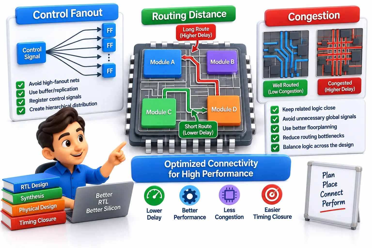
Not every timing failure comes from deep combinational logic. Sometimes the logic delay is relatively small while routing consumes much of the timing budget.
A signal driving hundreds of registers or blocks creates a high-fanout network. Enables, resets, mode controls and globally distributed status signals are common examples. The physical implementation tools must route these signals across significant portions of the design, potentially increasing delay and congestion.
Possible approaches include:
Replicating appropriate control logic
Registering control signals locally
Creating hierarchical distribution
Avoiding unnecessary global enables
Reducing excessive dependencies on one control signal
Keeping related processing stages architecturally localized
Physical awareness becomes increasingly important as designs grow. Two modules that look adjacent in RTL hierarchy are not necessarily physically close after placement.
This is why front-end and backend thinking cannot be completely separated. RTL determines connectivity, connectivity influences placement and routing, and routing affects timing.
A strong portfolio should demonstrate this connection. The Best RTL Design and Verification Projects to Build a Strong VLSI Career are projects where candidates can explain not only functionality but also architecture, timing constraints, critical paths, synthesis results and the optimization decisions they made.
Write RTL That Gives Synthesis Better Optimization Opportunities
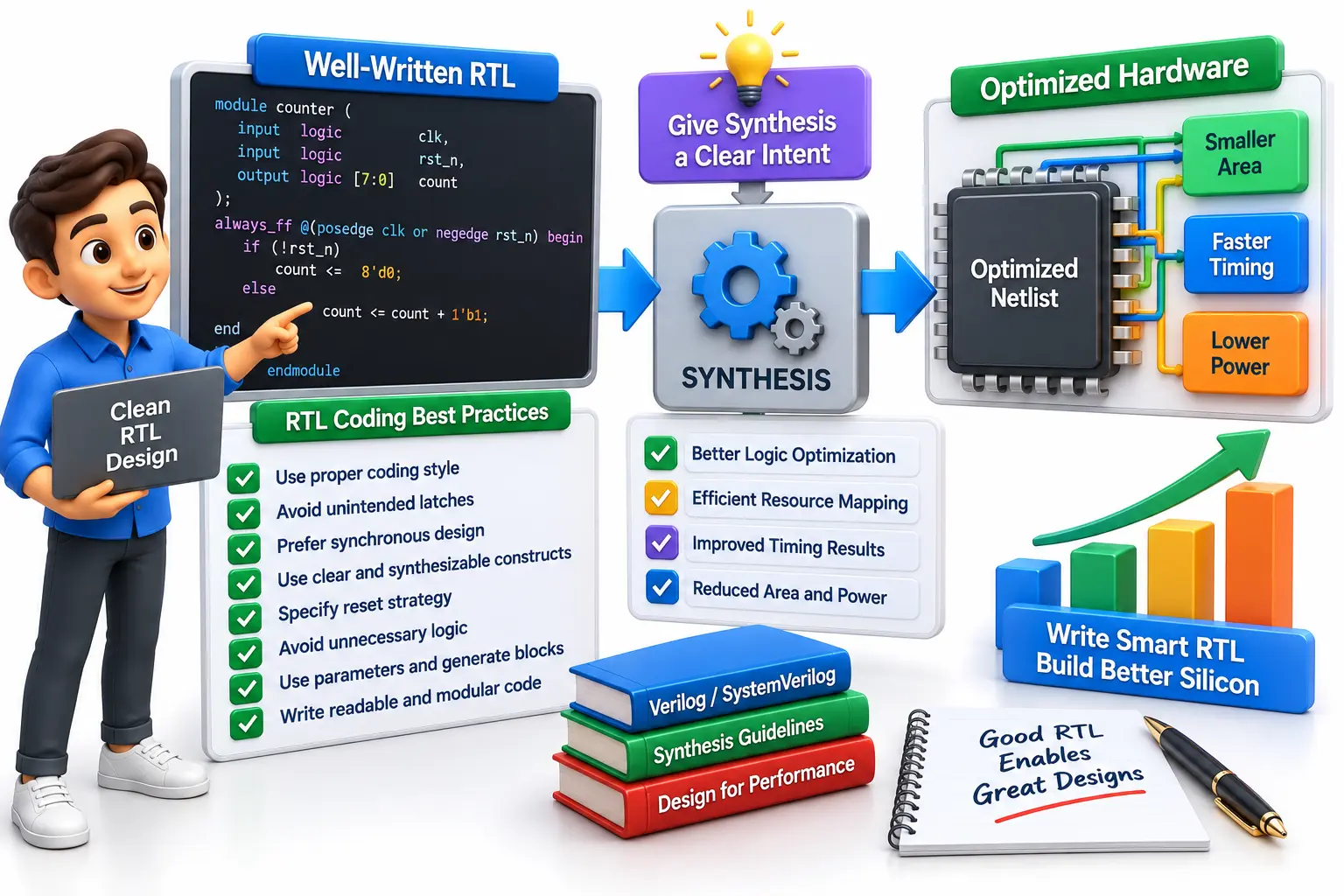
Synthesis tools are powerful, but they cannot rescue every inefficient architecture. Engineers should write RTL that communicates hardware intent clearly and avoids accidentally creating expensive structures.
One important example is resource sharing. Sharing an arithmetic unit can reduce area, but the multiplexers required to select its inputs may create additional timing pressure. Conversely, duplicating some logic can consume more area while producing faster paths. High-speed design constantly involves such performance-area-power trade-offs.
Engineers should also watch for unintended hardware:
Accidental priority logic
Unnecessary wide signals
Redundant arithmetic
Complex variable indexing
Inferred structures different from the intended architecture
Long dependency chains across modules
FSM design deserves similar attention. State encoding, next-state logic and output decoding can influence timing. There is no universal coding trick that makes every FSM faster; engineers must inspect what synthesis actually produced.
The key principle is simple: optimize inferred hardware, not the appearance of RTL source code.
Use Timing Reports as a Feedback Loop, Not Just a Final Check
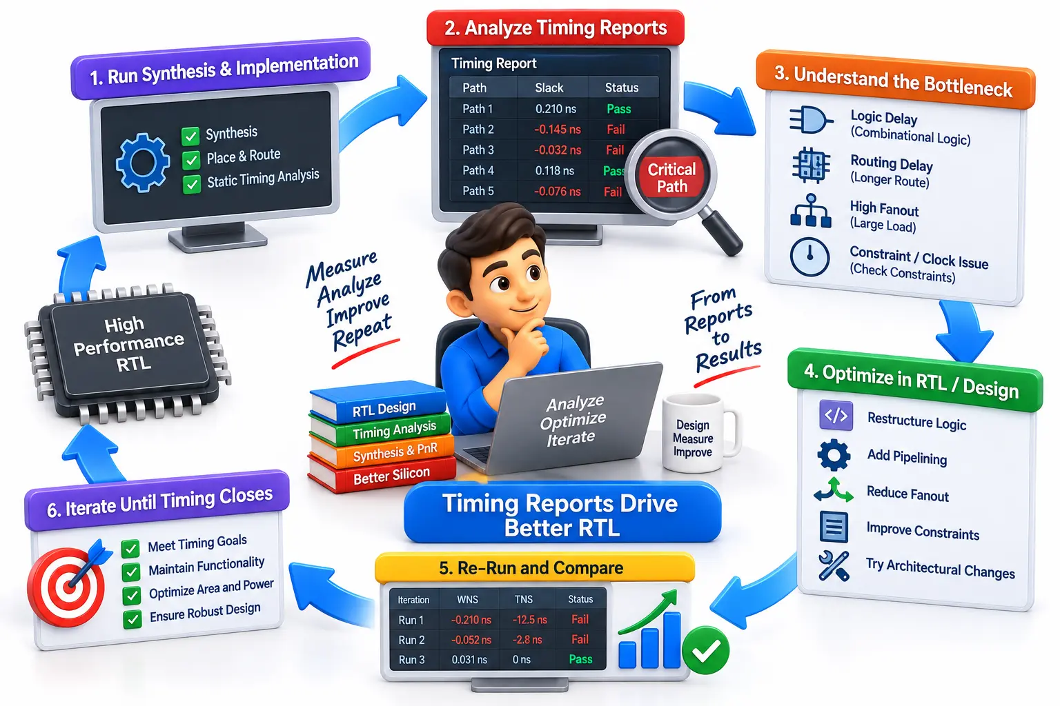
Timing optimization becomes much more effective when engineers stop guessing.
After synthesis and implementation, static timing analysis provides evidence about failing paths. Worst Negative Slack shows how badly the worst path misses its requirement, while Total Negative Slack helps indicate the broader scale of timing violations. Engineers should trace the actual startpoint, endpoint and delay components of problematic paths.
A disciplined optimization loop looks like this:
Confirm clocks and timing constraints are correct
Identify the worst failing path
Determine whether logic or routing dominates
Map the path back to the RTL architecture
Change one meaningful architectural factor
Re-run synthesis and implementation
Compare timing, area and functional results
Repeat until requirements are satisfied
Do not blindly optimize every path reported by a tool. Some paths may be incorrectly constrained, asynchronous, multicycle by design or otherwise require different treatment. Constraints must describe genuine design intent; false constraints can make reports look clean without making the hardware safe.
Timing closure is therefore iterative engineering. A change that fixes the current worst path may expose another path as the new bottleneck. Successful engineers keep measuring until the design converges rather than expecting one optimization to solve everything.
Conclusion
High-speed RTL design begins long before the final timing report. Pipeline boundaries, combinational depth, fanout, arithmetic architecture, control structures and module connectivity all influence whether the implemented circuit can operate at its target frequency. Timing closure becomes much more predictable when these decisions are made deliberately during RTL development.
For aspiring VLSI engineers, this skill also separates syntax knowledge from genuine engineering ability. Learn to read timing reports, connect violations back to RTL, modify the architecture and measure the result. That feedback loop is what turns functional RTL into implementation-ready high-performance hardware.