
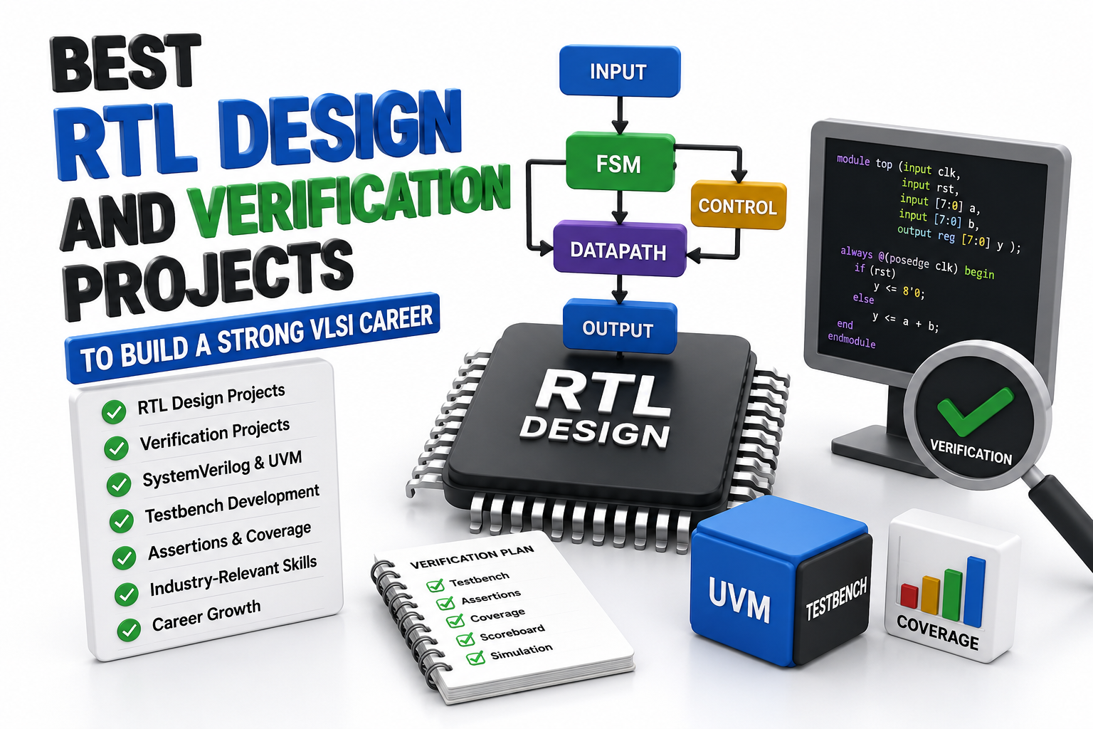
Best RTL Design and Verification Projects to Build a Strong VLSI Career
Navigate through this article using the table of contents below
Table of Contents
No headings found in this article.
Most VLSI aspirants make the same mistake: they complete a course, list 'Verilog' and 'SystemVerilog' on their resume, and wonder why interview calls never arrive. Here's the uncomfortable truth — semiconductor hiring managers at companies like Qualcomm, Intel, and Synopsys don't hire skill lists. They hire engineers who can demonstrate working RTL logic, clean testbenches, and real verification methodology. Your projects are the only proof they have before you walk into that room.
In India, the RTL design and verification training landscape has exploded, with institutes across Bangalore, Hyderabad, Noida, and Pune offering programs of varying depth. But very few guide students on which projects truly signal readiness to a recruiter. This guide fills that gap — breaking down 7 high-impact RTL design and verification projects, ranked by complexity, and explaining exactly what each one demonstrates to a hiring team. Whether you are just starting out or looking for structured RTL design and verification training in India, institutions like JastTech can help you build and execute these projects with industry mentorship.
UART Communication Controller — The Foundation Project
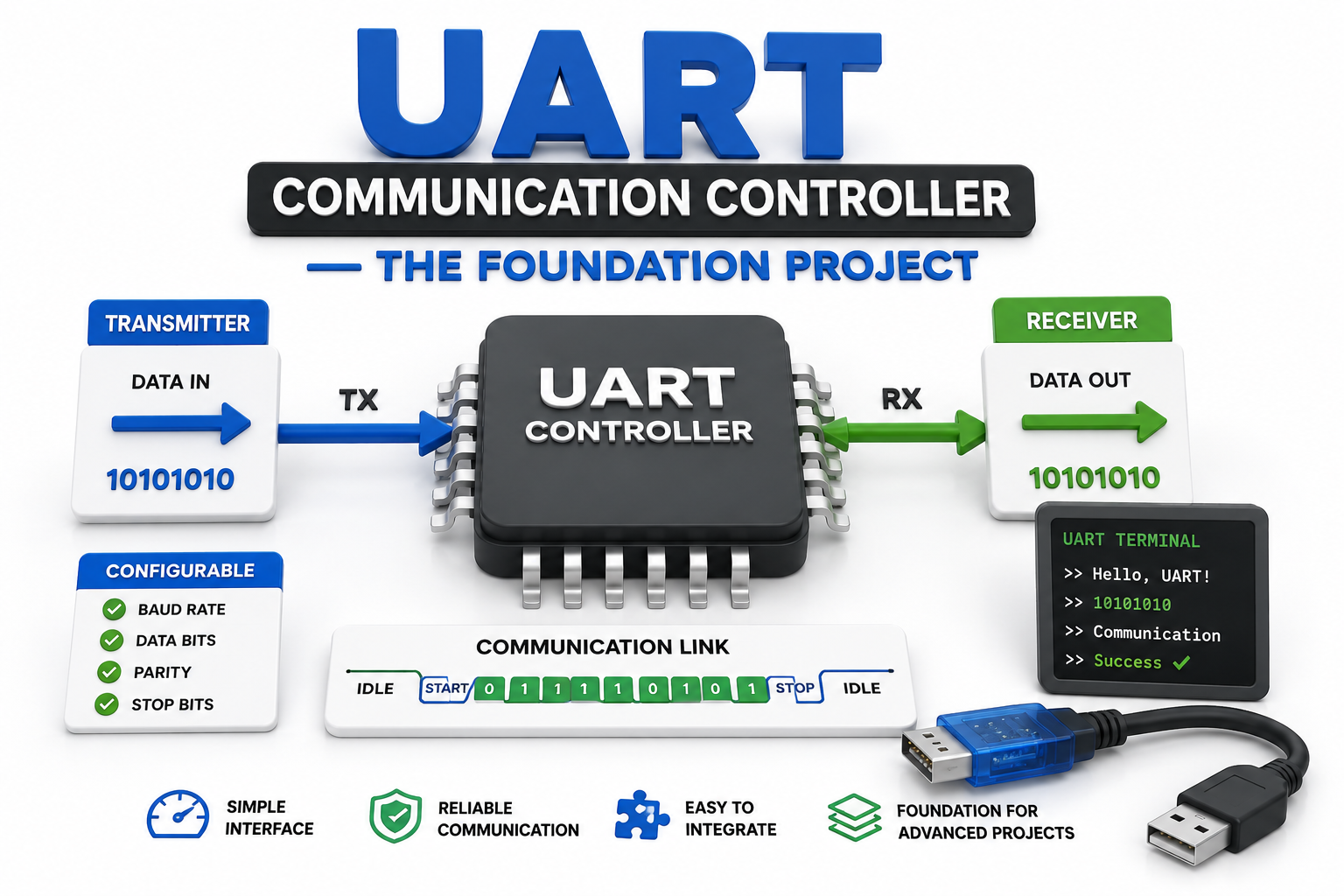
The Universal Asynchronous Receiver-Transmitter (UART) remains one of the most recruiter-recognized RTL projects, and for good reason. It combines sequential logic, finite state machines (FSMs), baud rate generation, and shift-register-based serial communication — all in a single, testable module. It is a direct test of your ability to write synthesizable Verilog that translates cleanly to hardware.
What makes a UART project stand out is not just coding the transmitter and receiver — it is the completeness of verification. Recruiters specifically look for:
• A directed testbench covering start bit, data bits, parity, and stop bit conditions
• Constrained-random test cases for baud rate tolerance and framing error injection
• Functional coverage points ensuring all state transitions are exercised
• Waveform capture using ModelSim or Questa showing correct timing
If you are pursuing RTL design and verification training in India, UART is almost always the first hands-on project assigned — and the depth to which you implement it tells your trainer (and future employer) everything about your approach to engineering rigor.
SPI Master-Slave Interface — Protocol and Timing Depth
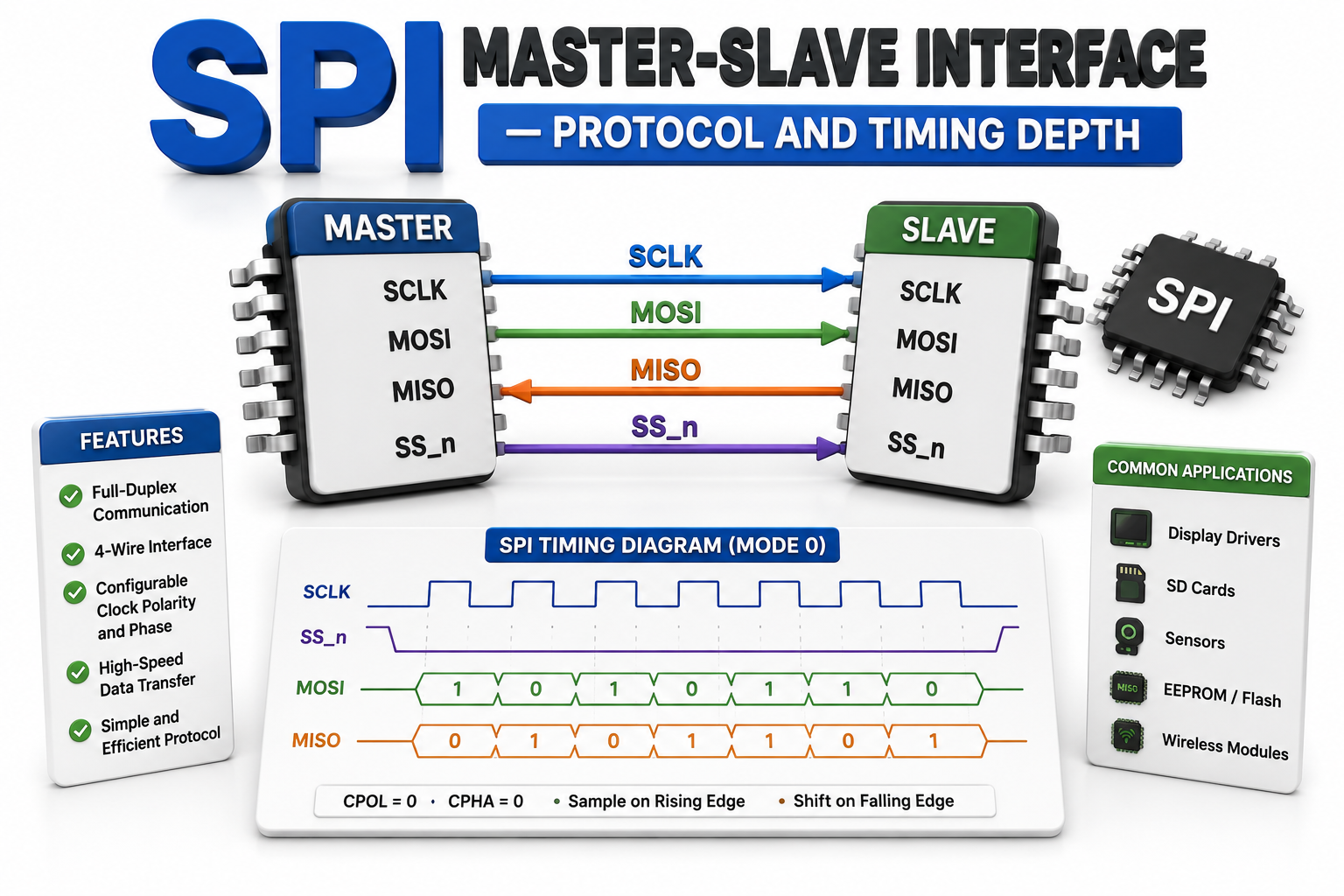
The Serial Peripheral Interface (SPI) project elevates your profile beyond UART by introducing clock polarity (CPOL), clock phase (CPHA), and multi-slave chip-select logic. These are real-world concerns in embedded SoC designs, and engineers who understand CPOL/CPHA configurations are immediately more valuable than those who do not.
A recruiter-ready SPI project includes three things most student implementations skip: a configurable data width register (not just 8-bit hardcoded), a loopback verification mode where master and slave self-check data integrity, and edge-case testing for mode switching without glitches. The SPI project also introduces you to the concept of interface timing diagrams — an absolute must for any RTL design and verification engineer working on chip integration teams.
Design both SPI master and slave in Verilog, not just one side
Include all four SPI modes (Mode 0 through Mode 3) with a mode-select register
Write a SystemVerilog assertion (SVA) to verify that MISO data is stable before rising clock edge
Host the project on GitHub with a clean README, block diagram, and waveform screenshots
Pipelined RISC Processor — The Career-Defining Project
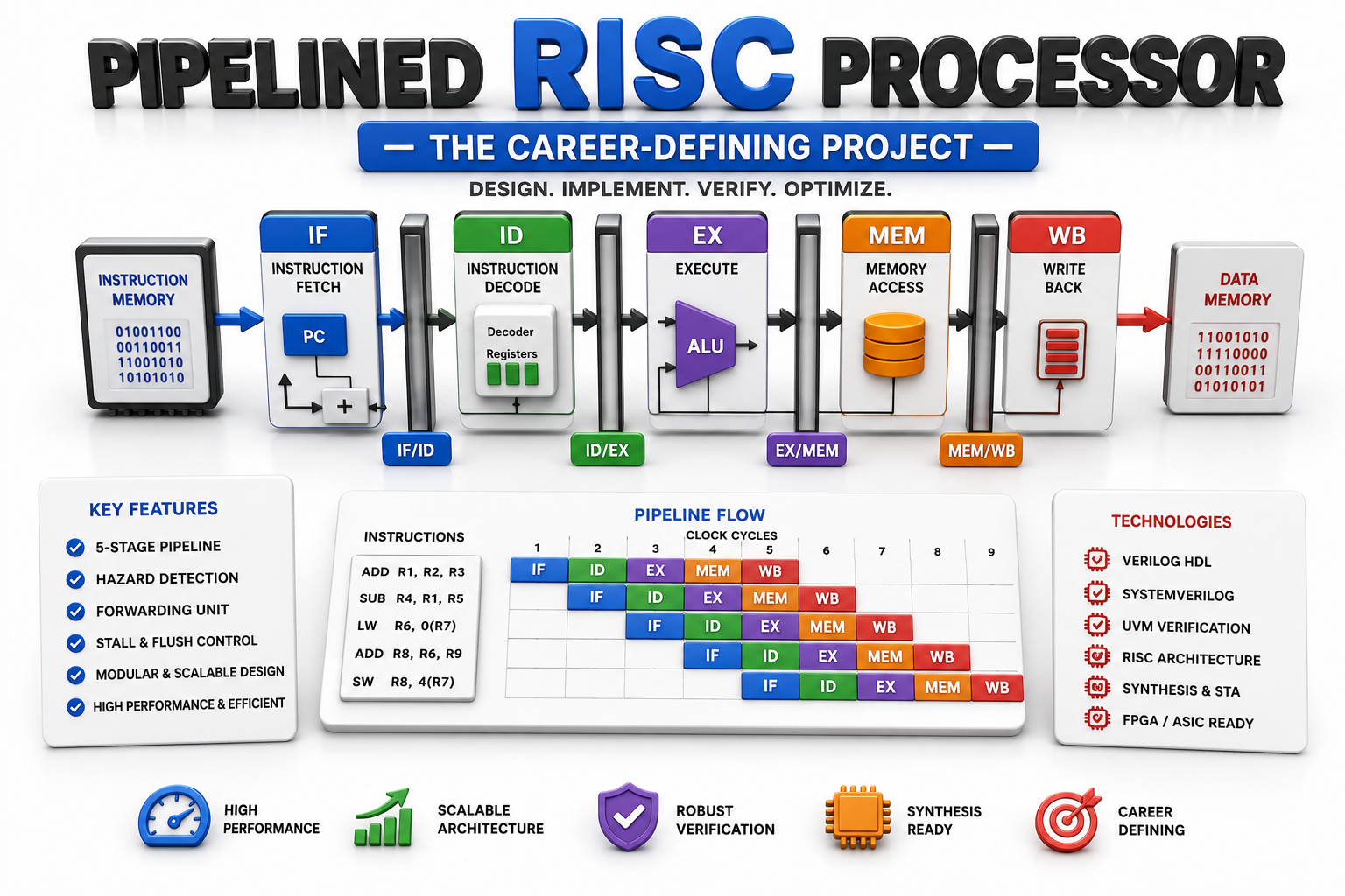
If UART gets you a screening call, a pipelined processor gets you a shortlist. A 5-stage pipelined RISC processor (Fetch, Decode, Execute, Memory, Writeback) is the single most comprehensive RTL project a fresher can build. It forces you to confront pipeline hazards — data hazards, control hazards, and structural hazards — and solve them architecturally. This is exactly the kind of thinking that ASIC and chip design companies want to see.
RTL design and verification in India has grown rapidly in part because companies like Intel Design Center in Bangalore, Qualcomm's Hyderabad office, and hundreds of VLSI startups now recruit specifically for processor microarchitecture awareness. A well-built RISC processor project on your resume opens doors to roles in CPU design, SoC verification, and even formal verification teams. JastTech's structured RTL design and verification training program walks learners through this project module-by-module, ensuring both the design and verification environments are industry-standard.
• Implement forwarding (bypassing) unit for data hazard resolution
• Add branch prediction logic, even a simple static predictor
• Write a UVM testbench with a scoreboard that cross-checks instruction results
• Synthesize with Synopsys DC or Vivado and report timing closure at a target frequency
Asynchronous FIFO with CDC — Showing You Understand Real Chip Challenges
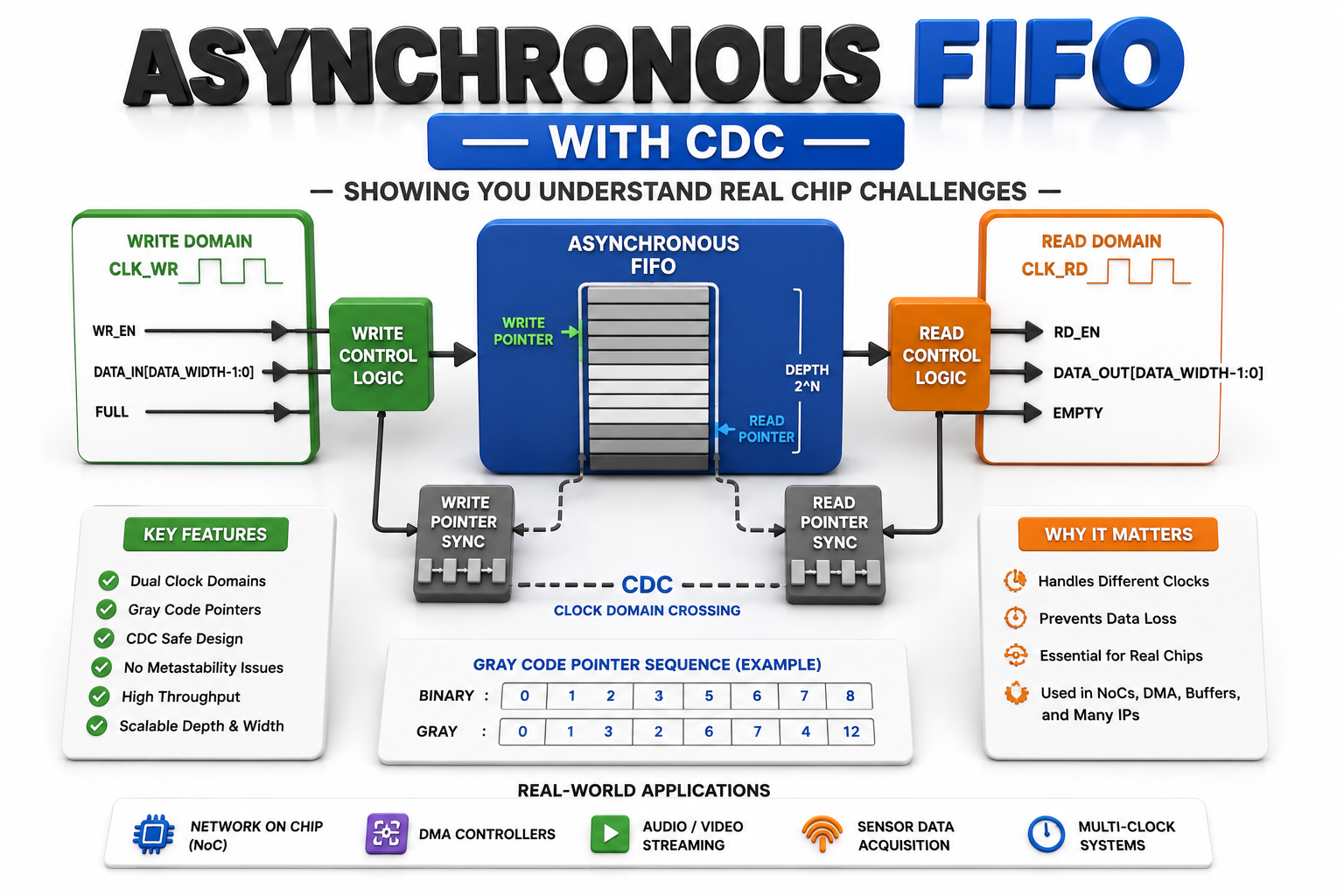
Clock Domain Crossing (CDC) is one of the most misunderstood topics in RTL design, and one of the most commonly tested in technical interviews. An Asynchronous FIFO project — where the write side operates on one clock and the read side on another — directly demonstrates your grasp of synchronization challenges that arise in every real SoC design.
Most beginner projects use synchronous FIFOs, which is fine for learning. But an asynchronous FIFO with gray-code pointer synchronization immediately signals that you understand the dangers of metastability, timing violations across clock domains, and the engineering solutions used in production silicon. This project is especially valuable if you are targeting verification engineer roles, as CDC verification is a specialized and high-demand skillset in India's VLSI job market.
• Use gray-code encoding for read/write pointers before passing them across clock domains
• Instantiate two-stage synchronizer flip-flops on both pointer paths
• Run a CDC analysis using Synopsys SpyGlass or Mentor Questa CDC
• Include full and empty flag logic with testbench cases for boundary conditions
AXI4 Slave Interface — Industry-Protocol Verification with UVM
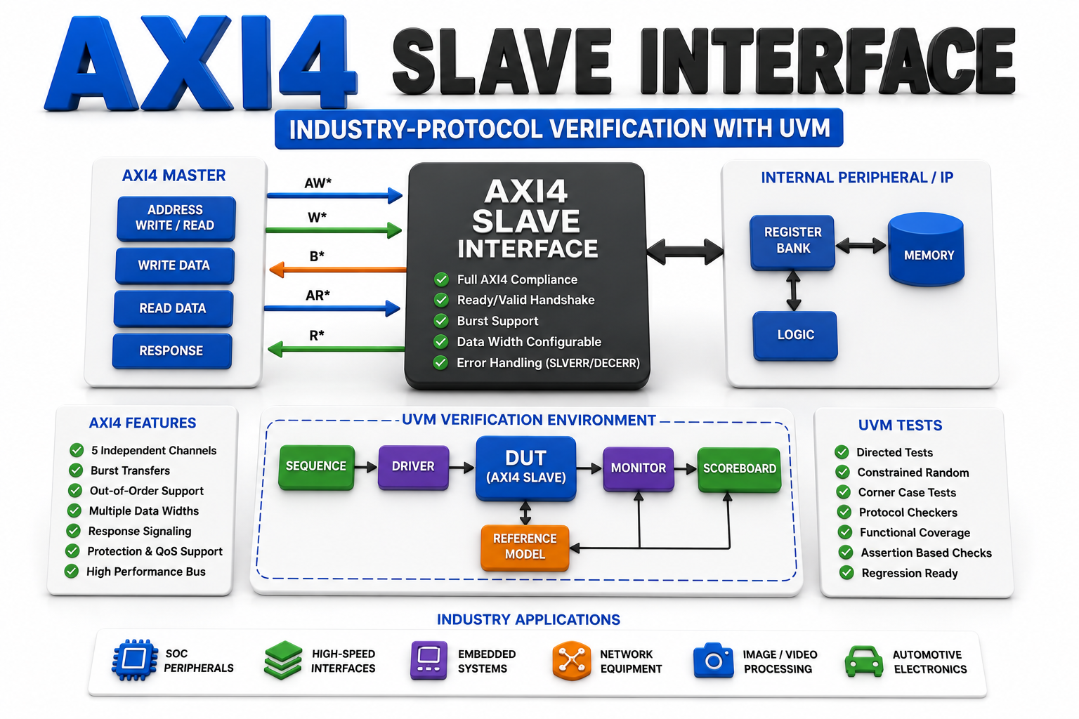
The AXI (Advanced eXtensible Interface) protocol from ARM is the dominant on-chip bus standard used in virtually every modern SoC. Designing and verifying an AXI4-Lite slave gives you direct exposure to handshaking, channel independence (write address, write data, write response, read address, read data channels), and protocol compliance — the exact things you will work on in your first industry role.
What makes AXI a standout project is that it practically demands a UVM verification environment. A complete AXI4 slave project includes a UVM agent with a driver, monitor, scoreboard, and coverage collector. This is what separates a resume that says 'knows UVM' from one that demonstrates it. In the context of RTL design and verification training in India, this is the project most institutes — including JastTech — use as a capstone, because it combines protocol knowledge, SystemVerilog proficiency, and UVM methodology into a single deliverable.
• Implement read and write channels with proper VALID/READY handshake logic
• Create a UVM sequence library with directed and constrained-random scenarios
• Add protocol checkers as SystemVerilog Assertions bound to the interface
• Generate a coverage report showing 90%+ functional coverage closure
Memory Controller with Refresh Logic — Deep Verification Complexity
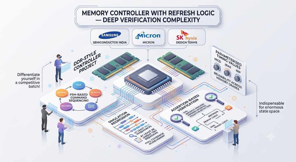
A DDR-style memory controller project — even a simplified LPDDR-like implementation — is one of the hardest and most impressive projects an RTL engineer can put in a portfolio. It requires handling timed refresh cycles, burst read/write sequencing, row activation and precharge logic, and timing parameter awareness (tRCD, tRAS, tRP). This directly maps to the real-world work done at companies like Samsung Semiconductor India, Micron, and SK Hynix's design teams.
From a verification standpoint, memory controllers are notoriously difficult to achieve full coverage on because the state space is enormous. This is where assertion-based verification becomes indispensable. Writing SVA properties that check refresh interval compliance, burst ordering, and error response behavior demonstrates a maturity of verification thinking that few freshers possess. If you are enrolled in RTL design and verification training in India and want to differentiate yourself in a competitive batch, this is the project to pursue.
• Implement FSM-based command sequencing: IDLE, ACTIVATE, READ/WRITE, PRECHARGE, REFRESH
• Parameterize timing values (tRCD, tRAS, tRP) for reusability across memory grades
• Write SVA to enforce minimum refresh interval violation detection
• Run simulation regression with at least 50 unique test sequences
Conclusion
In conclusion, breaking into the competitive VLSI industry requires far more than theoretical knowledge or superficial course certifications. To truly attract the attention of hiring managers at top-tier firms like Qualcomm and Intel, you must transcend the generic skill lists on your resume and present tangible proof of your engineering capabilities. The five high-impact projects detailed in this guide—ranging from the foundational UART to the complex Memory Controller—are designed to demonstrate your ability to write clean, synthesizable RTL logic and implement mature, comprehensive verification methodologies.
Building these projects and documenting them thoroughly, ideally on platforms like GitHub with clear READMEs, block diagrams, and waveform screenshots, creates a compelling portfolio that signals interview-readiness to any recruiter. For aspiring VLSI engineers seeking deep, structured RTL design and verification training in India with experienced industry mentorship, institutions like JastTech provide the ideal environment to construct, execute, and refine these portfolio-defining projects. Don't wait to be asked; let your work do the talking and open the doors to a successful career in chip design.