

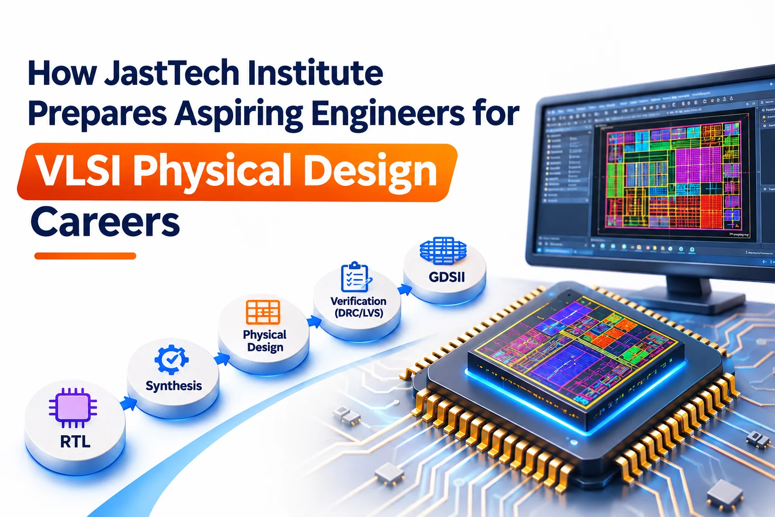
How JastTech Institute Prepares Aspiring Engineers for VLSI Physical Design Careers
Navigate through this article using the table of contents below
Table of Contents
No headings found in this article.
A semiconductor chip may look like a tiny piece of silicon, but creating it requires thousands of engineering decisions. Behind every successful chip is a physical design process that transforms logical circuits into manufacturable layouts. Are you prepared to enter this highly specialized engineering field?
Physical design offers exciting opportunities for electronics graduates who enjoy solving complex technical problems. However, academic knowledge alone is rarely enough. JastTech focuses on connecting engineering fundamentals with practical implementation skills to help aspiring professionals prepare for semiconductor industry opportunities.
Understanding the Complete RTL-to-GDSII Design Flow
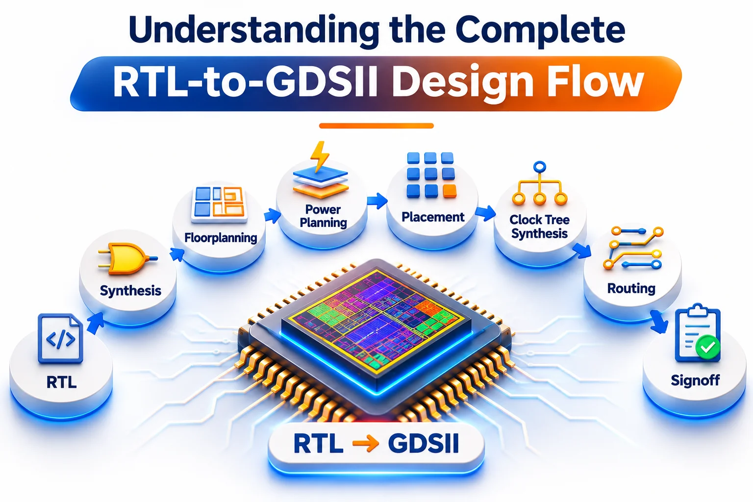
Physical design is a critical stage in the ASIC development process. It begins after logic synthesis generates a gate-level netlist and converts the logical representation into a physical layout suitable for semiconductor manufacturing.
Engineers must understand how different implementation stages influence power, performance and area (PPA). A decision made during floorplanning can affect placement congestion, routing complexity and timing closure later in the flow.
JastTech introduces learners to the complete physical design workflow, helping them understand the relationship between individual stages.
The major stages include:
Synthesis: Converts RTL descriptions into optimized gate-level netlists.
Floorplanning: Establishes chip dimensions, macro locations and initial physical organization.
Power Planning: Creates power distribution networks to supply stable power.
Placement: Positions standard cells while considering timing and congestion.
Clock Tree Synthesis: Builds the clock distribution network while controlling skew and latency.
Routing: Establishes electrical connections between physical components.
Signoff: Checks timing, physical verification and other implementation requirements.
Understanding this complete process helps students recognize that physical design is not simply about placing cells. Every stage involves engineering decisions that influence the final chip.
Building Strong Foundations in Digital Electronics and Timing Analysis
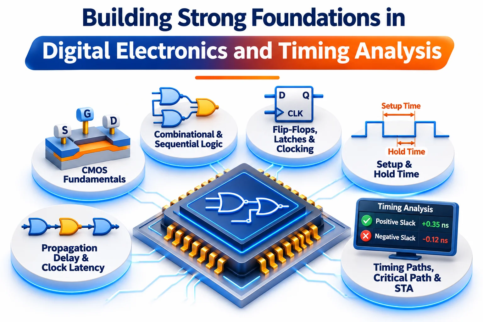
A successful physical design engineer needs more than familiarity with implementation software. Strong digital electronics and semiconductor fundamentals are essential for understanding why implementation problems occur.
JastTech emphasizes foundational knowledge that helps students understand the behavior of digital circuits and the timing requirements of synchronous systems.
Important concepts include:
CMOS fundamentals and standard cell architecture.
Combinational and sequential logic.
Flip-flops, latches and clocking concepts.
Setup time and hold time requirements.
Propagation delay and clock latency.
Timing paths and critical path identification.
Basic Verilog concepts and synthesis fundamentals.
Static Timing Analysis (STA) is particularly important because physical design engineers continuously evaluate whether signals reach their destinations within the required timing limits.
Students need to understand positive and negative slack, clock uncertainty, setup violations and hold violations.
For example, if a critical path fails setup timing after placement, an engineer must examine cell delay, interconnect delay, fanout and physical distance. Depending on the cause, optimization may involve cell resizing, buffering or placement improvements.
This analytical approach develops the problem-solving mindset expected from professional backend engineers.
Learning Industry-Relevant Physical Design Tools and Technologies
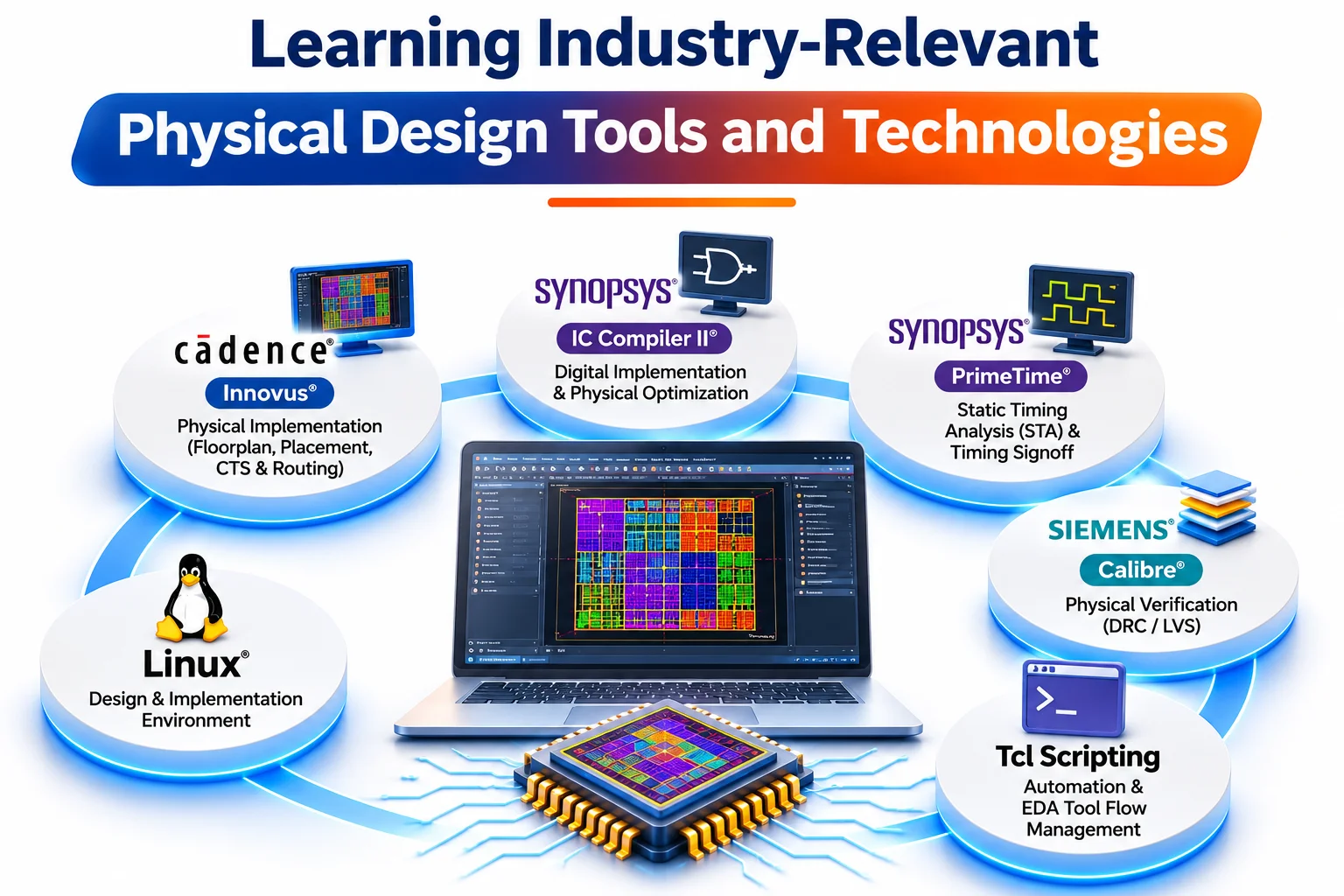
EDA tools are essential for implementing and optimizing modern semiconductor designs. However, simply knowing tool names does not make someone industry-ready. Engineers must understand the commands, reports and optimization decisions involved in actual implementation.
JastTech incorporates exposure to industry-standard tool families into its physical design learning approach.
Important technologies include:
Cadence Innovus: Used for physical implementation activities, including floorplanning, placement, CTS and routing.
Synopsys IC Compiler II: Supports digital implementation and physical optimization.
Synopsys PrimeTime: Used for static timing analysis and timing signoff.
Siemens Calibre: Supports physical verification activities such as DRC and LVS.
Linux: Provides the command-line environment commonly used in semiconductor design workflows.
Tcl Scripting: Helps automate repetitive implementation tasks and manage EDA tool operations.
Students also need to become comfortable interpreting implementation reports rather than depending entirely on automated tool results.
For instance, a congestion report can reveal areas where routing resources are insufficient. A timing report helps identify critical paths, while physical verification reports highlight layout rule or connectivity violations.
Learning to interpret these outputs helps aspiring engineers understand the reasoning behind implementation decisions.
Developing Practical Skills Through Industry-Oriented Projects
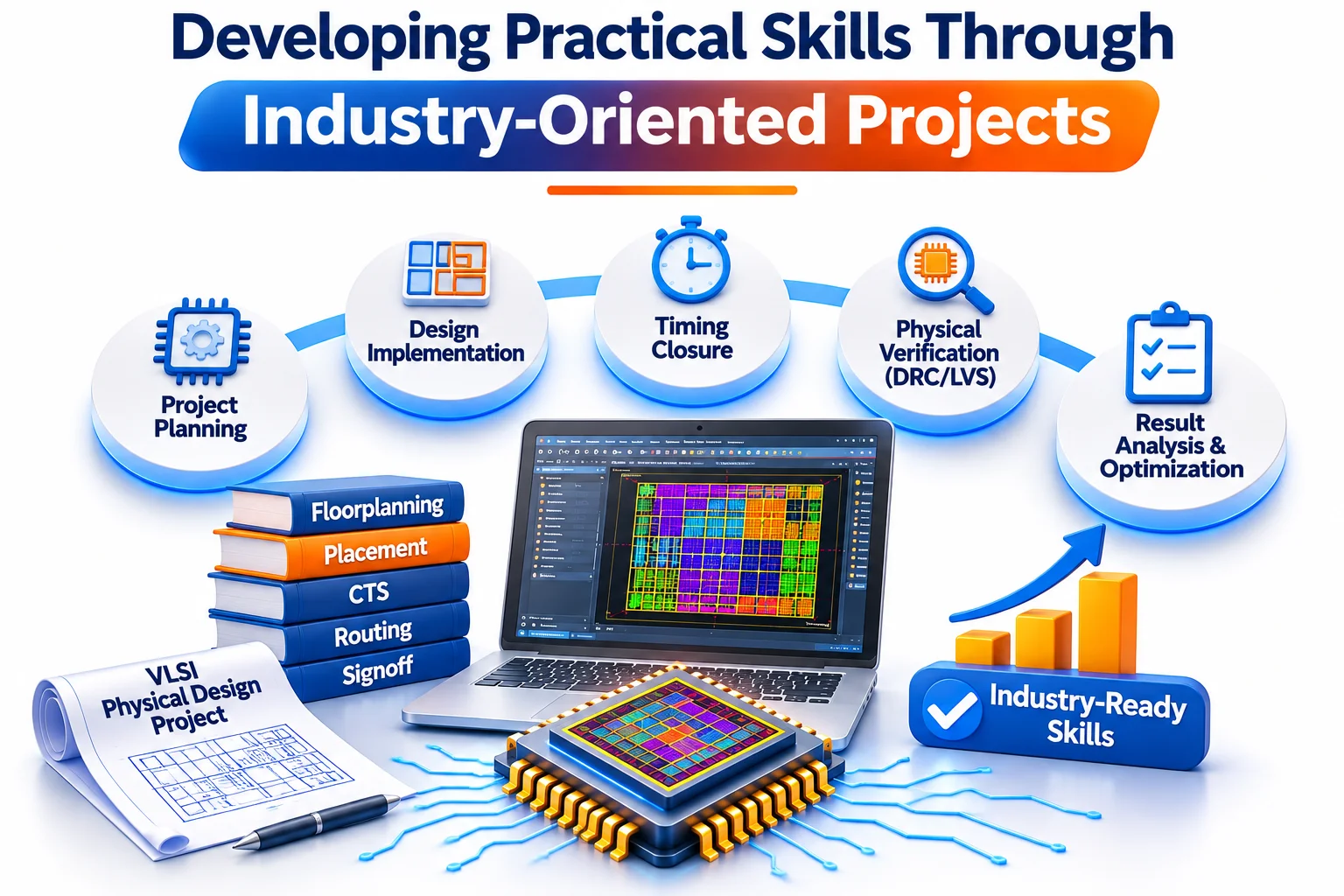
One of the biggest challenges for VLSI freshers is the difference between understanding theoretical concepts and applying them to actual engineering problems.
Practical projects help bridge this gap by allowing learners to experience the complete implementation process.
JastTech incorporates project-oriented learning into its training approach, including physical design activities that help students understand real implementation requirements.
Examples of relevant project areas include:
Low-Power ASIC Physical Design
Students explore floorplanning, power planning and placement while considering area utilization, power distribution and timing requirements.
Placement and Timing Optimization
Learners examine placement results, identify critical timing paths and understand optimization techniques for addressing setup violations.
Clock Tree Synthesis and Timing Closure
Students study clock distribution, insertion delay, clock skew and hold timing challenges after CTS.
RTL-to-GDSII Implementation
A complete implementation exercise helps learners understand how synthesis outputs progress through floorplanning, placement, clock tree synthesis, routing and final verification.
During these projects, students should focus on documenting:
Design inputs and implementation objectives.
Constraints and technology files.
Placement and routing results.
Timing reports and optimization decisions.
DRC and LVS verification outcomes.
A documented project provides stronger evidence of technical understanding than simply mentioning software tools on a resume.
Preparing Engineers for Semiconductor Industry Interviews and Careers
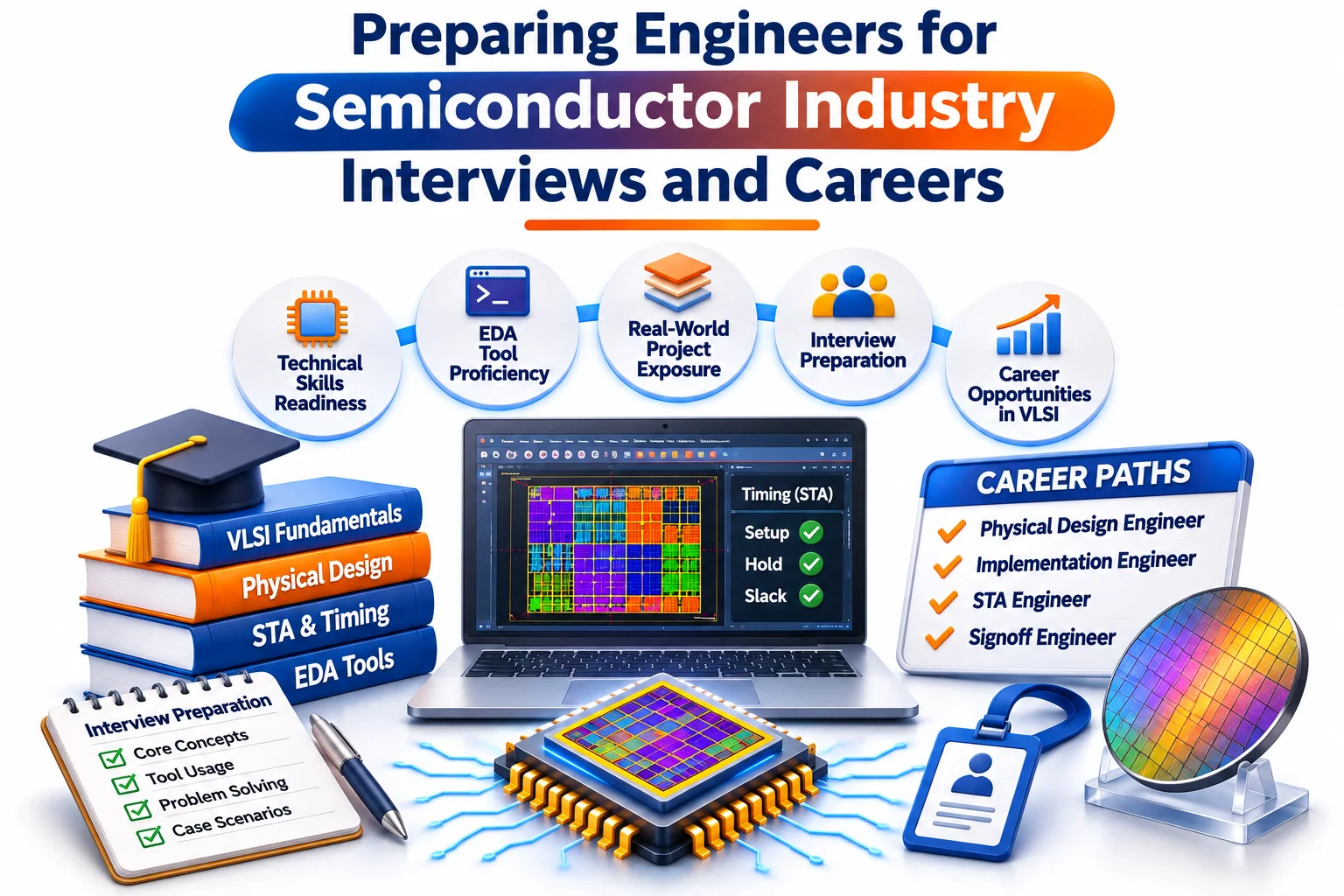
Technical knowledge must be communicated effectively during interviews. Semiconductor recruiters often evaluate whether candidates understand implementation concepts and can explain how they approach engineering problems.
JastTech supports career preparation through activities such as resume development, LinkedIn profile guidance, mock interviews, technical mentoring and placement assistance.
Aspiring engineers should prepare for questions covering several important areas:
What is the difference between floorplanning and placement?
How does clock skew influence setup and hold timing?
What causes congestion during physical implementation?
How do you identify a critical path using STA reports?
What happens during clock tree synthesis?
What is the difference between DRC and LVS?
How can placement optimization improve timing?
Candidates should also learn to explain their project decisions instead of memorizing definitions.
For example, when discussing a timing violation, an engineer should explain how the violation was identified, which report was analyzed, what caused the problem and which optimization technique was selected.
With structured technical preparation and project experience, learners can target entry-level opportunities such as:
Physical Design Engineer
Physical Design Trainee
Backend VLSI Engineer
Place and Route Engineer
Static Timing Analysis Engineer
Physical Verification Engineer
Career progression depends on technical ability, practical experience, project complexity and employer requirements.
Why JastTech Is a Learning Destination for Aspiring VLSI Engineers
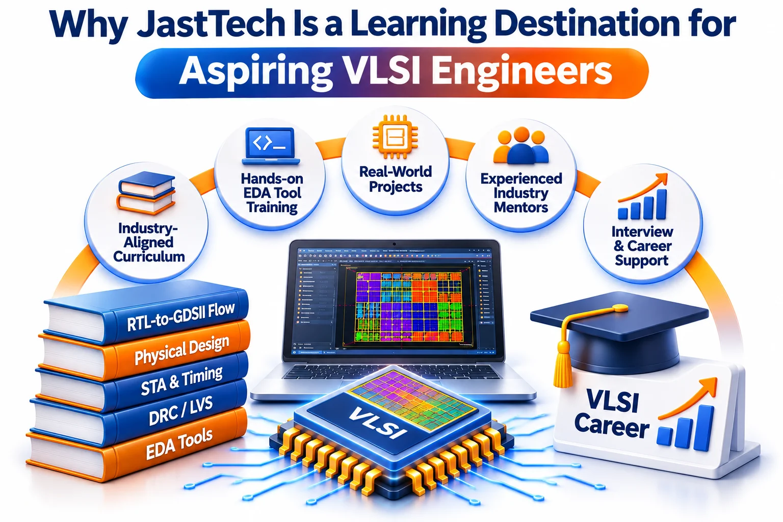
Choosing the right training environment is an important decision for engineering graduates. A useful program should combine technical fundamentals, implementation practice, mentorship and career preparation rather than focusing exclusively on classroom explanations.
JastTech aims to connect these learning requirements through its structured semiconductor training programs.
Its physical design curriculum covers the major backend implementation stages, including floorplanning, power planning, placement, CTS, routing, static timing analysis and physical verification.
The learning approach also incorporates practical projects and exposure to commonly used EDA tool families. This gives students opportunities to understand implementation workflows and develop technical confidence.
For candidates comparing a VLSI Training Institute in India, important factors include curriculum depth, practical tool exposure, mentor support, project quality and interview preparation.
JastTech also provides additional career-oriented support, including resume assistance, mock interviews, LinkedIn profile guidance and placement support.
However, students should remember that completing a course does not automatically guarantee employment. Consistent practice, strong fundamentals, independent debugging ability and interview performance remain essential.
Conclusion
Physical design is an exciting career direction for electronics graduates interested in semiconductor engineering. However, entering this field requires a combination of digital fundamentals, timing analysis, EDA tool knowledge and practical implementation experience. Understanding the complete RTL-to-GDSII flow helps aspiring engineers develop the technical foundation required for backend VLSI opportunities.
JastTech aims to prepare aspiring professionals through structured Physical Design Training, practical projects, industry-oriented tool exposure and career guidance. For students who want to move beyond theoretical electronics knowledge and develop specialized semiconductor skills, choosing the right learning program can be an important first step toward building a rewarding physical design career.