

How to Become a VLSI Engineer in Noida: Step-by-Step Guide
Navigate through this article using the table of contents below
Table of Contents
No headings found in this article.
The Indian semiconductor industry is expanding rapidly, and Noida has become one of the country's most promising destinations for electronics and chip design professionals. Companies are actively seeking engineers who possess practical skills rather than only academic knowledge.
If you want to build a rewarding career in chip design, simply earning an engineering degree is no longer enough. Success depends on following the right learning path, mastering industry tools, building practical experience, and preparing strategically for technical interviews. This guide explains every step required to become a successful VLSI engineer in Noida.
Understand the Fundamentals of VLSI Design Before Choosing Your Specialization
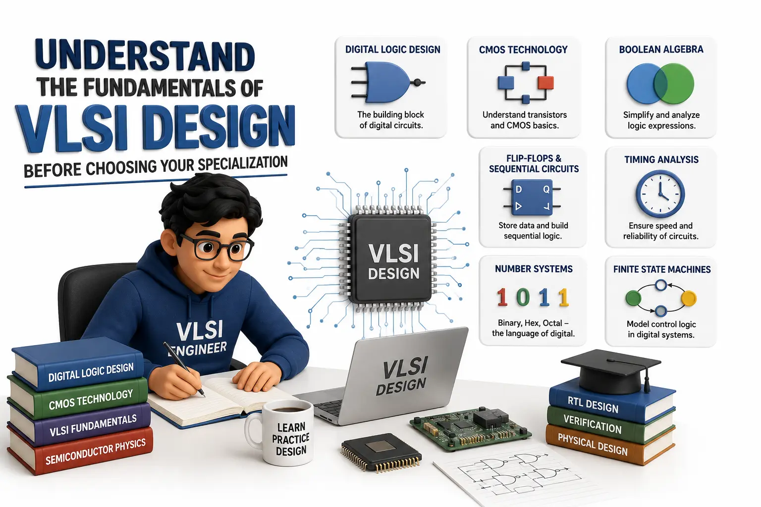
Every successful VLSI engineer begins with a strong understanding of digital electronics and semiconductor fundamentals. These concepts form the foundation for every design, verification, and implementation activity throughout a professional career.
Students should first develop confidence in subjects such as:
Digital Logic Design
CMOS Technology
Boolean Algebra
Flip-Flops and Sequential Circuits
Timing Analysis
Number Systems
Finite State Machines
Once these fundamentals become clear, understanding advanced concepts like RTL Design, Functional Verification, Static Timing Analysis, or Physical Design becomes significantly easier. Strong fundamentals also help during technical interviews, where recruiters often evaluate conceptual understanding before testing tool knowledge.
Choose the Right Learning Path That Matches Industry Requirements
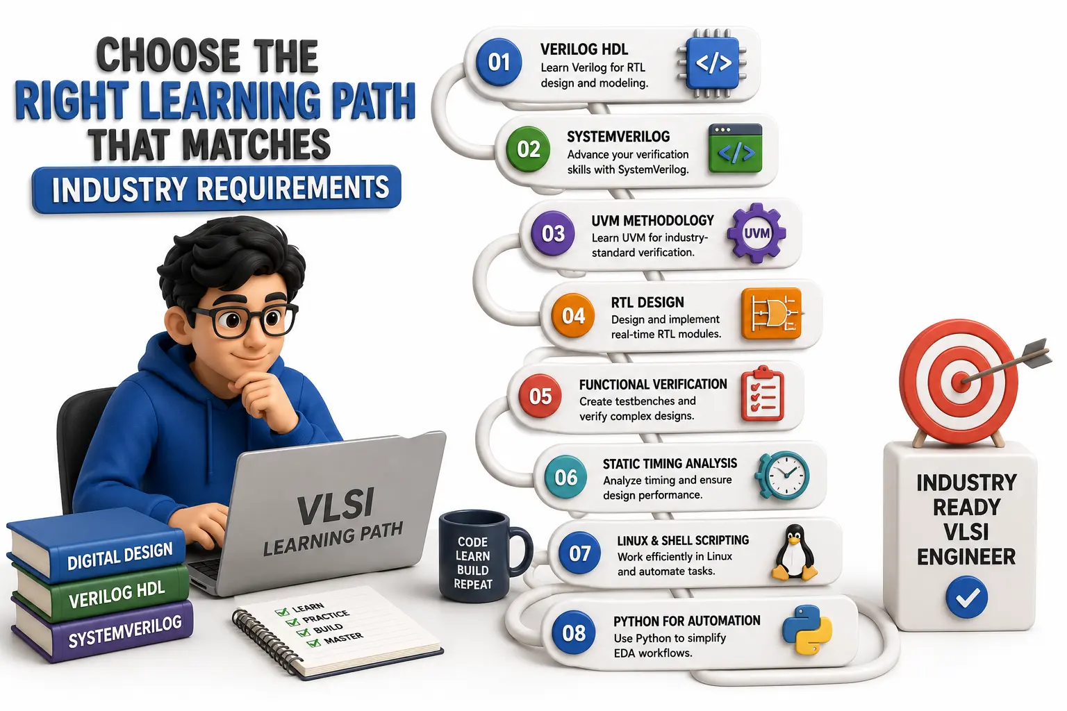
After building theoretical knowledge, the next step is selecting a structured learning path aligned with current hiring expectations. Many fresh graduates spend months studying random online content without gaining practical expertise.
A professional learning roadmap should include:
Verilog HDL
SystemVerilog
UVM Methodology
RTL Design
Functional Verification
Static Timing Analysis
Physical Design Basics
Linux Commands
Shell Scripting
Python for Automation
Students searching for a vlsi course in noida should evaluate whether the curriculum includes hands-on projects, real EDA tools, mentorship, and placement assistance rather than focusing only on classroom lectures. A structured learning environment helps bridge the gap between academics and industry expectations.
Master Industry Tools Through Practical Projects
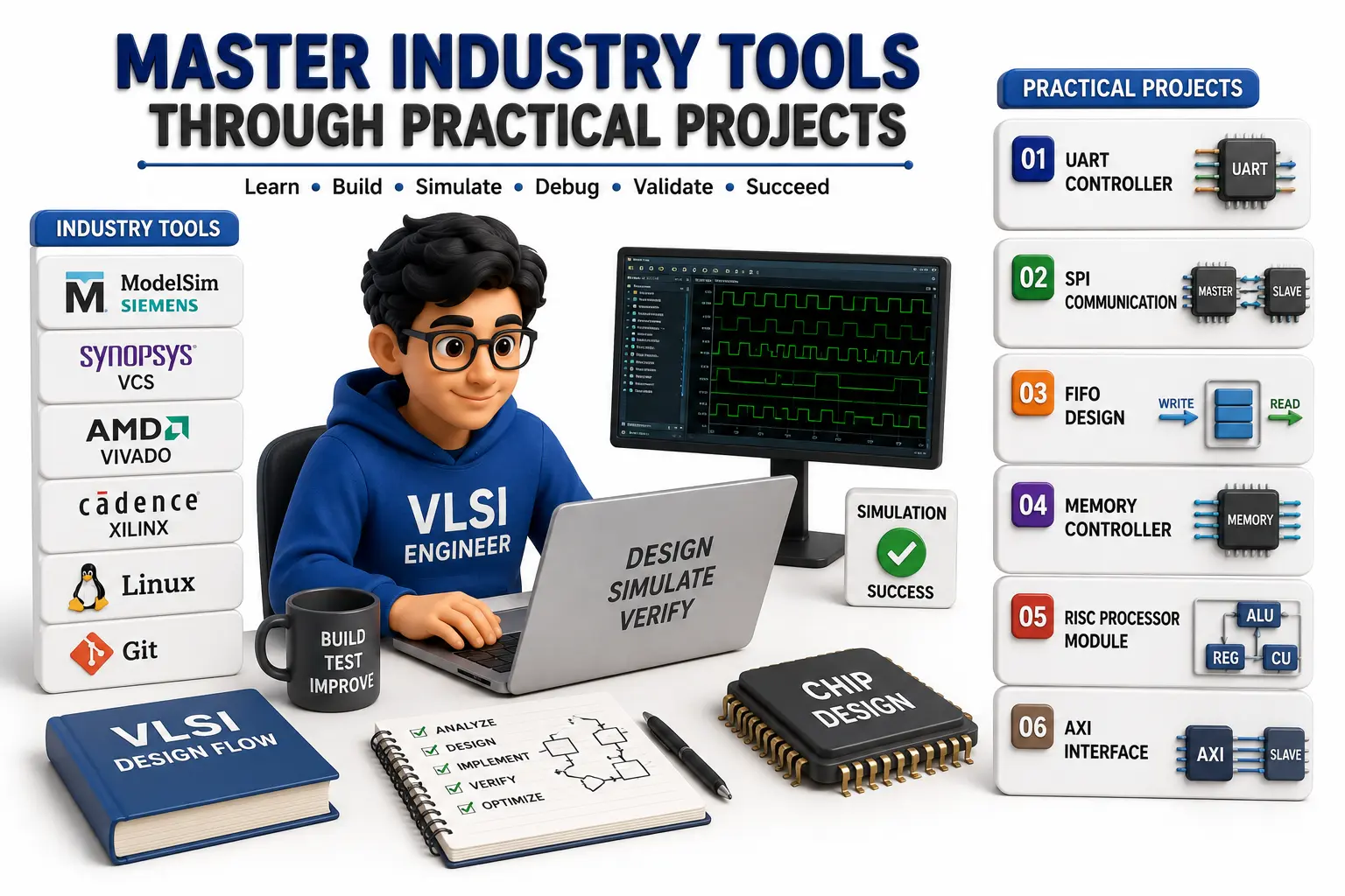
The semiconductor industry values engineers who can demonstrate practical implementation rather than theoretical knowledge alone. Recruiters frequently ask candidates to explain projects, debug designs, and describe their development process during interviews.
Practical experience should include working on projects such as:
UART Controller
SPI Communication Protocol
FIFO Design
Memory Controller
RISC Processor Modules
AXI Interface
ALU Design
Along with project development, students should become familiar with commonly used EDA environments, simulation workflows, waveform debugging, synthesis concepts, and version control practices.
Hands-on learning develops confidence, improves debugging ability, and prepares candidates for real engineering responsibilities after joining a semiconductor company.
Build an Interview-Ready Portfolio That Demonstrates Real Skills
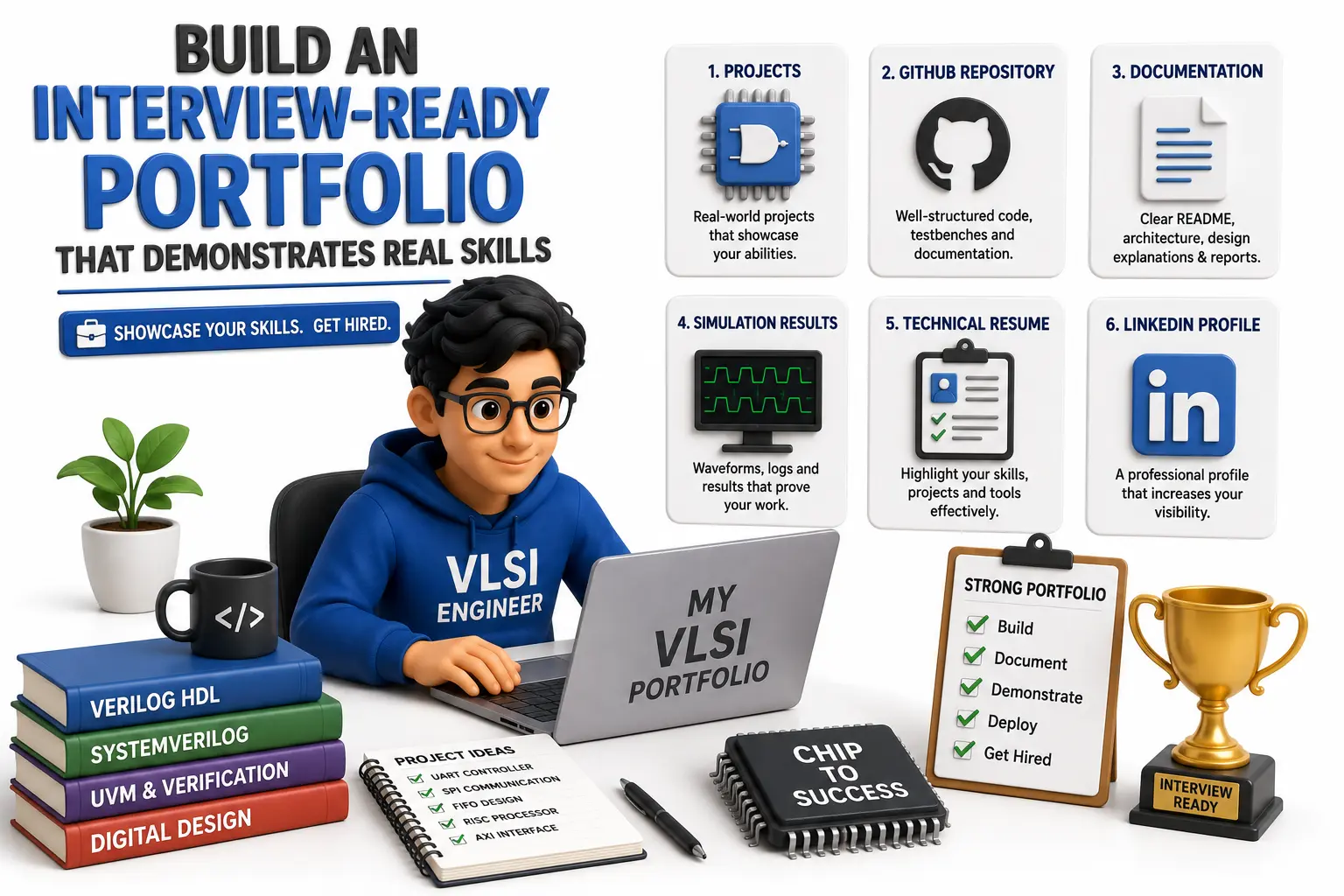
A strong portfolio often creates a better first impression than a lengthy resume. Recruiters prefer candidates who can clearly demonstrate what they have designed, verified, and implemented.
An effective technical portfolio should contain:
RTL Design projects
Verification testbenches
GitHub repository
Documentation for every project
Simulation waveforms
Design reports
Resume highlighting technical skills
Professional LinkedIn profile
Students enrolling in vlsi training in noida should ensure they graduate with multiple industry-level projects rather than only completion certificates. Employers increasingly evaluate practical evidence of technical ability before scheduling interviews.
A well-organized portfolio also helps candidates confidently explain design decisions, debugging approaches, and verification strategies during technical discussions.
Prepare Systematically for Technical Interviews
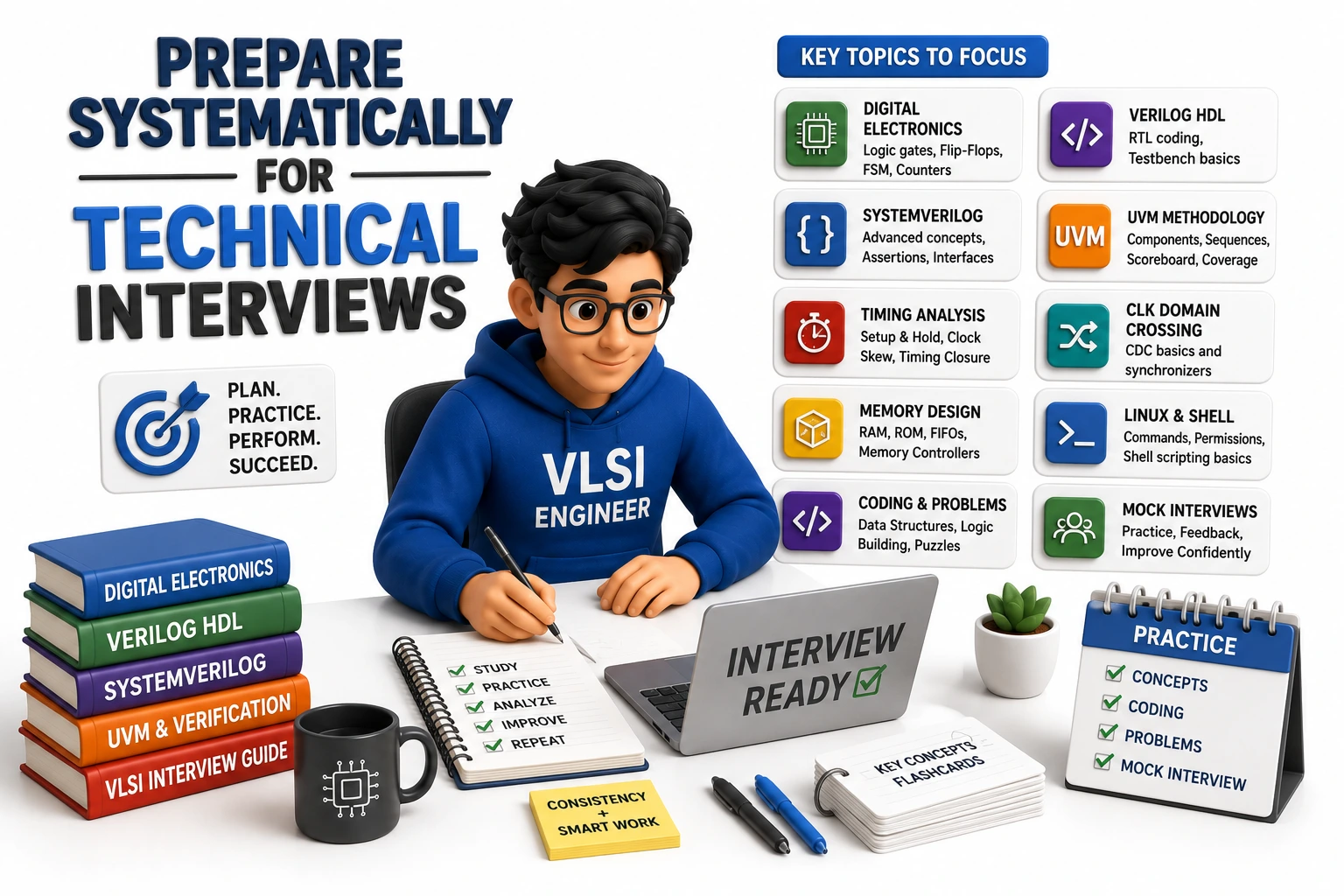
Interview preparation should begin long before submitting job applications. Semiconductor interviews typically assess conceptual understanding, coding ability, problem-solving skills, and communication.
Candidates should regularly practice topics including:
Digital Electronics
Verilog Coding
SystemVerilog Concepts
Timing Analysis
FSM Design
Setup and Hold Violations
Clock Domain Crossing
Memory Design
RTL Coding Questions
Linux Commands
Basic Python Problems
Mock interviews provide valuable experience by exposing knowledge gaps before actual recruitment processes. Candidates should also practice explaining every project confidently, including architecture, implementation challenges, debugging techniques, and optimization decisions.
Consistent preparation significantly improves interview performance while reducing anxiety during technical discussions.
Apply Strategically and Continue Learning After Your First Job
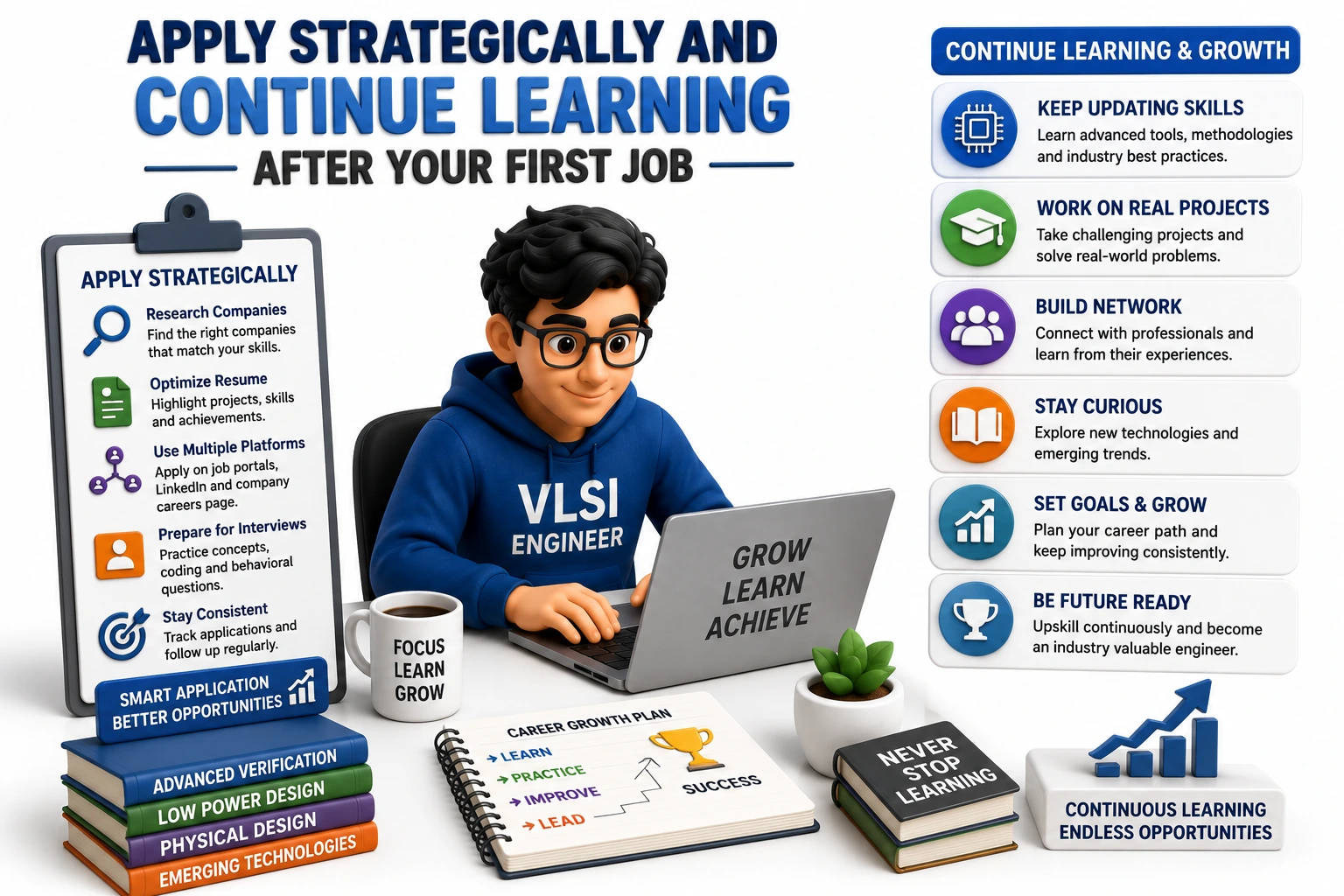
Landing the first job marks the beginning of a VLSI career rather than its final destination. The semiconductor industry evolves rapidly, making continuous learning essential for long-term growth.
Graduates should regularly:
Follow semiconductor industry developments
Learn advanced verification methodologies
Explore AI-assisted chip design workflows
Study low-power design techniques
Improve scripting and automation skills
Participate in technical communities
Build increasingly complex projects
Choosing a reputed vlsi training institute in noida can provide valuable industry exposure, mentorship, interview guidance, and networking opportunities that accelerate career growth during the early stages of professional development.
Continuous improvement allows engineers to transition from entry-level roles into specialized positions such as RTL Design Engineer, Verification Engineer, Physical Design Engineer, DFT Engineer, or Design Automation Engineer as their experience grows.
Conclusion
Building a successful VLSI career requires much more than completing an engineering degree. It demands a structured approach that combines strong theoretical knowledge, practical implementation, project development, industry tools, interview preparation, and continuous learning. Engineers who consistently build these competencies position themselves for long-term success in India's expanding semiconductor ecosystem.
At JastTech, aspiring semiconductor professionals can follow an industry-focused learning path designed to bridge the gap between academic education and real-world hiring expectations. With hands-on projects, expert mentorship, modern design methodologies, and interview-oriented preparation, students can confidently develop the skills required to pursue rewarding opportunities in Noida's rapidly growing VLSI industry and build a sustainable career in semiconductor engineering.