

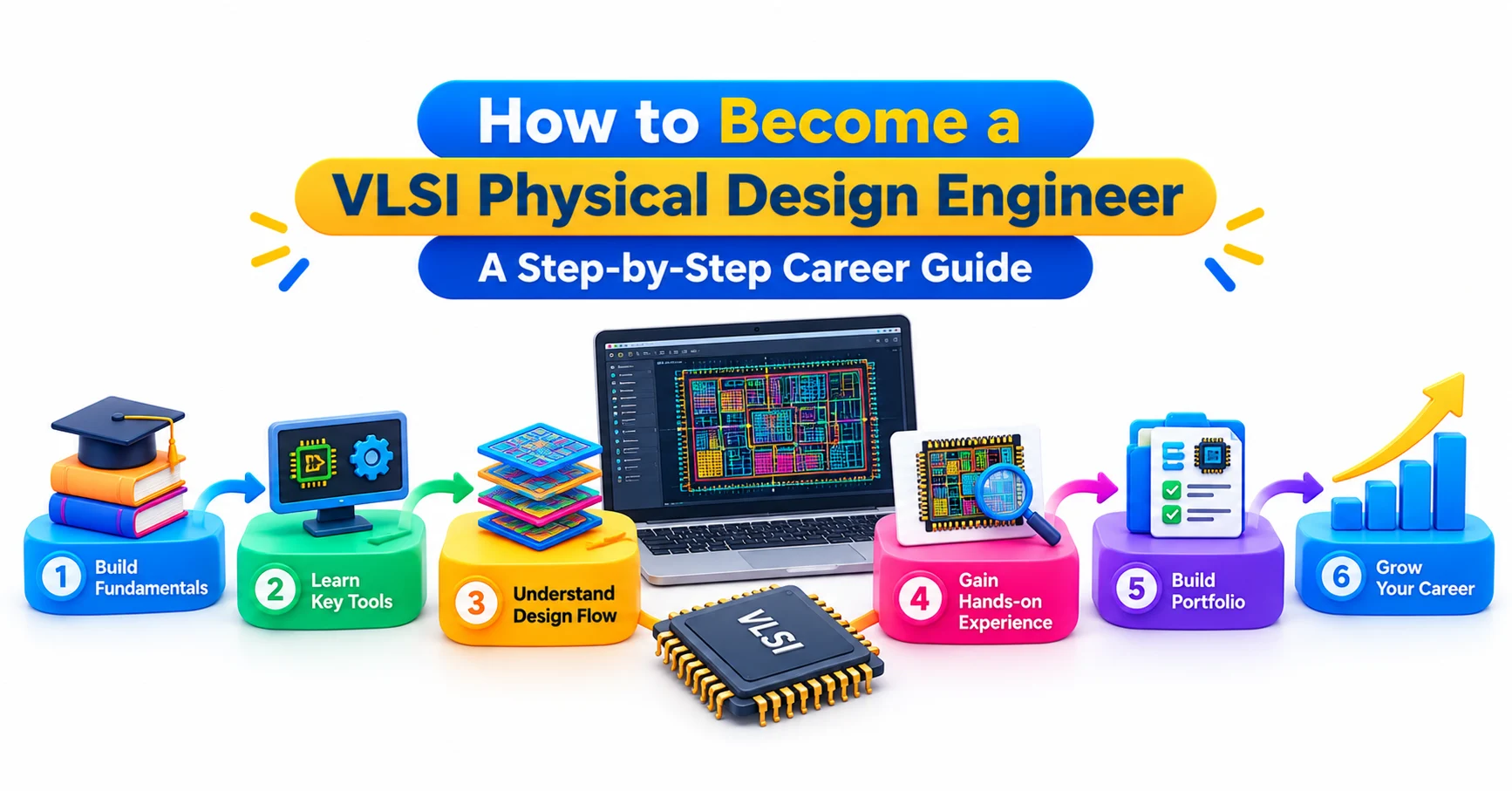
How to Become a VLSI Physical Design Engineer: A Step-by-Step Career Guide
Navigate through this article using the table of contents below
Table of Contents
No headings found in this article.
A chip with billions of transistors does not become a working product because someone drew it neatly. It works because a physical design team made thousands of small trade-offs between speed, power and area, and made them correctly. If you want to know how to become a VLSI physical design engineer, the path is clearer than most people expect, and a structured physical design training program can shorten the learning curve considerably.
The harder question is what to learn first, what to skip, and how to prove you can do the job before anyone has hired you.
What a VLSI Physical Design Engineer Actually Does All Day

A VLSI physical design engineer takes a verified logic design, usually delivered as a gate-level netlist, and turns it into a physical layout that can be manufactured. Think of it as city planning for silicon: the netlist says which buildings exist and who talks to whom, and the physical design engineer decides where everything sits, how the roads connect it, and whether the power grid can keep every district lit.
In practice the day is less glamorous than that sounds. You run a step of the flow, read the reports, and find out why something failed. A typical morning might involve a block with negative slack on a handful of critical paths, a congestion hotspot near a memory macro, or a clock tree with too much skew. Much of the job is diagnosis.
Physical design sits between front-end design and manufacturing. RTL designers and verification engineers hand over a design, and the physical design team has to close timing, power and design rules before it goes to the foundry as a final layout file. Because it touches so many constraints at once, the role rewards people who enjoy debugging systems rather than writing one clever block.
Teams usually split the work by block or by stage. Some engineers own a full block from floorplan to signoff, while others specialise in clock tree synthesis, static timing analysis, or physical verification. Early in a career you will probably see a slice of everything, which is useful.
The Foundation: Degrees, Subjects and Skills You Need First

Most physical design engineers hold a bachelor’s or master’s degree in electronics, electrical engineering, or a closely related field. Computer science graduates also enter the field, though they usually need to catch up on device physics and digital circuits. The degree matters less than being able to show the underlying knowledge.
Start with digital electronics. You should be comfortable with combinational and sequential logic, setup and hold time, flip-flops, latches, and finite state machines. Timing concepts show up in every stage of physical design, so shaky fundamentals here will slow you down later.
Next comes CMOS basics: how an inverter works, what drives delay, why power has dynamic and leakage components, and how wire resistance and capacitance affect signals as geometries shrink. You do not need to be a device physicist, but you must understand why a long wire behaves differently from a short one.
Then add a working picture of the VLSI design flow. Know what RTL, synthesis, DFT and verification do, because physical design inherits their output and their problems. A netlist with poor synthesis constraints will fight you at every step.
Finally, build scripting skills early. Tcl is the language of most commercial EDA tools, and Python or Perl helps with report parsing and automation. Many beginners treat scripting as optional, then discover that nearly every real task involves it. A practical habit is to write a small script for anything you do more than twice.
Soft skills matter more than job posts suggest. Patience, careful reading of logs, and the ability to explain a timing problem to a colleague who owns a different block will help you more than memorising command syntax.
Learning the Physical Design Flow Stage by Stage
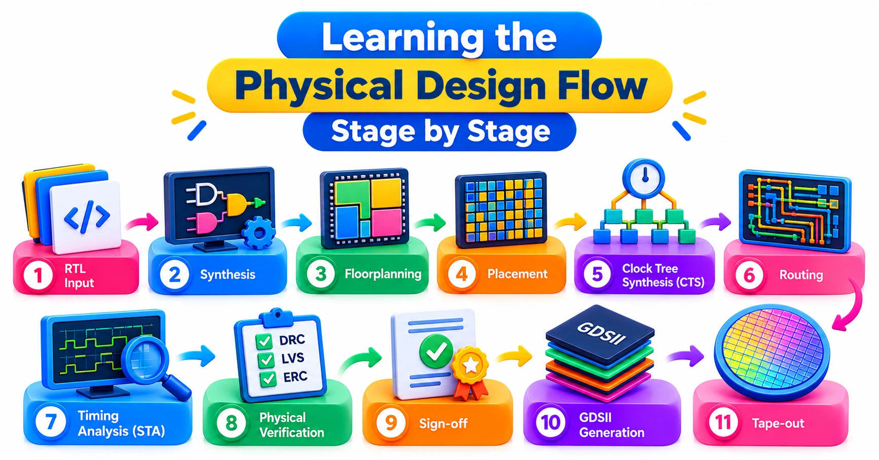
The flow is the heart of the career, and it is easiest to learn as a chain where each stage inherits the mistakes of the one before. Here is the sequence you need to understand deeply.
Floorplanning decides the die size, the placement of macros such as memories and analog blocks, the I/O pin locations, and the power grid structure. Poor macro placement is one of the most common causes of problems that show up much later as congestion or timing failures. Beginners often rush this step, then spend days fixing what a better floorplan would have prevented.
Placement positions the standard cells. The tool balances wirelength, timing and congestion, and you guide it with constraints, utilisation targets and blockages. Optimisation steps then resize cells, insert buffers, and fix design rule violations such as maximum transition and capacitance.
Clock tree synthesis builds the network that delivers the clock to every flip-flop with controlled skew and latency. It changes timing for the whole design, which is why you re-check setup and hold afterwards. Understanding useful skew, clock gating and clock domain crossings separates a competent engineer from someone who only runs scripts.
Routing connects the placed cells using metal layers and vias, first globally and then in detail. This is where crosstalk, antenna violations and DRC errors appear, and where congestion planned for in the floorplan finally pays off or backfires.
Signoff is where the design is judged. Static timing analysis checks setup and hold across multiple corners and modes. Physical verification runs DRC and LVS to confirm the layout obeys foundry rules and matches the schematic. Power analysis covers IR drop and electromigration. Engineering change orders, usually called ECOs, let you fix late problems without redoing the whole flow.
Learn each stage by asking three questions: what goes in, what comes out, and what can go wrong. That framing also happens to be how interviewers think.
Tools, Scripting and Technology Nodes: What to Practise Hands-On
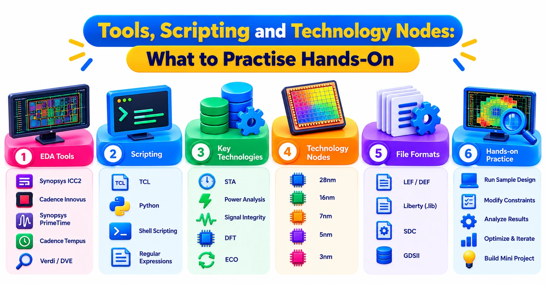
Reading about the flow is not the same as running it. Employers hiring freshers want to see that you have touched the tools, even on small designs.
The commercial tools you will meet most often come from Cadence and Synopsys. Cadence Innovus and Synopsys IC Compiler II, along with the newer Fusion Compiler environment, handle place and route. Synopsys PrimeTime is widely used for static timing signoff, while Siemens Calibre is a common choice for physical verification. Access to these tools is usually through a university lab, an employer, or a training institute, because licences are expensive.
If you cannot get commercial access, the open-source route is genuinely useful. OpenROAD, together with open process kits such as SkyWater 130nm, lets you take a small design from RTL to a GDSII layout on your own machine. The interface differs from commercial tools, but the concepts, including floorplan, placement, CTS, routing and timing reports, transfer directly.
Practise reading the files that drive the flow. Liberty files describe cell timing, LEF and DEF describe the physical library and the design database, and SDC files carry timing constraints. A surprising number of failures come from a wrong constraint rather than a wrong layout, so being able to read an SDC file with confidence is a real advantage.
Technology node awareness also helps. At advanced nodes, engineers deal with FinFET devices, multiple patterning rules, stricter design rules and heavier variation effects. You will not master all of it as a beginner, but knowing why lower nodes make timing closure and power integrity harder shows that you understand the direction of the industry.
A good practice routine is simple. Pick a small block, run the full flow, then deliberately break something: tighten the clock, raise utilisation, or move a macro. Watching how the reports change teaches you more than a clean run ever will.
Building Projects and a Portfolio That Recruiters Believe

Recruiters reading physical design resumes see the same line repeatedly: “completed project on floorplanning and placement.” It tells them nothing. What convinces them is specificity.
A strong project states the design, the technology, the tool, and the measurable result. For example, a block taken through the flow with setup and hold violations reduced to zero, DRC and LVS clean, and a short note on what you changed to get there. If you used an open-source flow, say so plainly. Honest scope beats inflated claims, and interviewers will probe whatever you list.
Document the problems, not only the outcome. A one-page write-up explaining why congestion appeared near a macro, what you tried, and what finally worked demonstrates exactly the thinking employers want. Keep these notes on a public repository or a simple portfolio page.
Several project ideas suit beginners:
Take a small RISC-V core or a similar open design through floorplanning, placement, clock tree synthesis and routing
Close timing on a block by experimenting with clock period, utilisation and cell sizing
Build a Tcl or Python script that parses timing reports and summarises the worst violating paths
Run an IR drop analysis and explain how changing the power grid affects it
Certifications and course completion help, but they are supporting evidence rather than proof of skill. Training that includes real design flows and tool practice carries more weight than a certificate alone, which is one reason JastTech structures its physical design learning around hands-on flow work instead of theory only.
Do not ignore the fundamentals while building projects. Many candidates can run a flow yet cannot explain why hold fixing adds delay buffers or why a clock tree changes slack. That gap shows quickly in conversation.
Becoming a VLSI Physical Design Engineer: Interviews, First Job and Growth Path
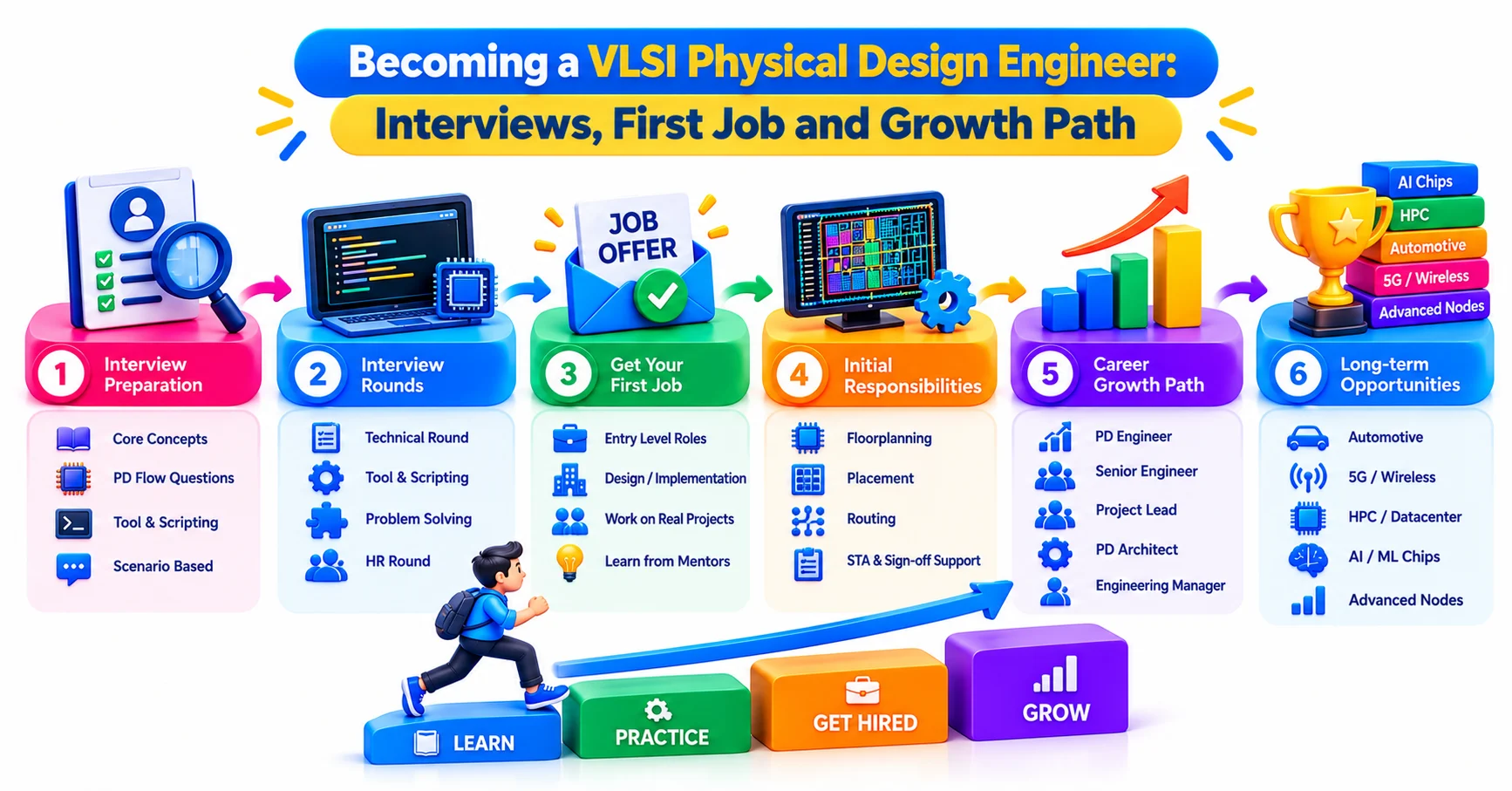
Interviews for entry-level physical design roles tend to start with fundamentals and move toward the flow. Expect questions on setup and hold, clock skew, congestion, utilisation, crosstalk, antenna effects, and how you would fix a timing violation. Reviewing common physical design interview questions is a practical way to find your weak spots before an interviewer does.
When you answer, explain your reasoning rather than reciting definitions. If asked how to fix a setup violation, walk through the options: sizing up cells, restructuring logic, adjusting clock skew, or changing placement. Then mention the cost of each, such as power or area. Interviewers listen for trade-offs.
The first job is usually in a physical design or implementation team at a semiconductor company, a design services firm, or an EDA-related organisation. Early work often involves block-level tasks, running flows under supervision, fixing violations, and supporting ECOs. It can feel repetitive at first, but it builds the pattern recognition that experienced engineers rely on.
Growth follows a fairly natural pattern. With experience you take ownership of larger blocks, then full chip integration, then technical leadership of a team or specialisation in an area such as timing signoff, power integrity, or advanced node methodology. Some engineers move into CAD or flow development, where they automate and improve the methodology itself.
Be realistic about the timeline. Learning the flow takes months of consistent practice, and real fluency takes years of working on actual tapeouts. The field rewards persistence, and progress feels slow right until concepts begin to connect.
Conclusion
Becoming a VLSI physical design engineer comes down to solid fundamentals, a deep understanding of the flow, hands-on tool practice, and projects you can explain honestly. None of it requires genius, only steady practice and curiosity about why a design fails. Start small, break things on purpose, and learn from every report. The engineers who get hired are rarely the ones who know the most terms, but the ones who can reason through a problem.