

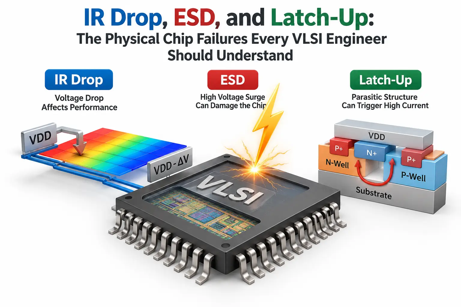
IR Drop, ESD, and Latch-Up: The Physical Chip Failures Every VLSI Engineer Should Understand
Navigate through this article using the table of contents below
Table of Contents
No headings found in this article.
A chip can pass RTL simulation, achieve timing closure and survive thousands of verification tests—and still fail after fabrication. Why? Because silicon must obey electrical and physical laws that digital simulation can sometimes make easy to overlook.
Three problems every VLSI engineer should recognize are IR drop, electrostatic discharge (ESD), and latch-up. They arise differently, but each demonstrates the same lesson: designing correct logic is only part of designing a reliable chip.
Understand Why a Logically Correct Chip Can Still Fail Physically
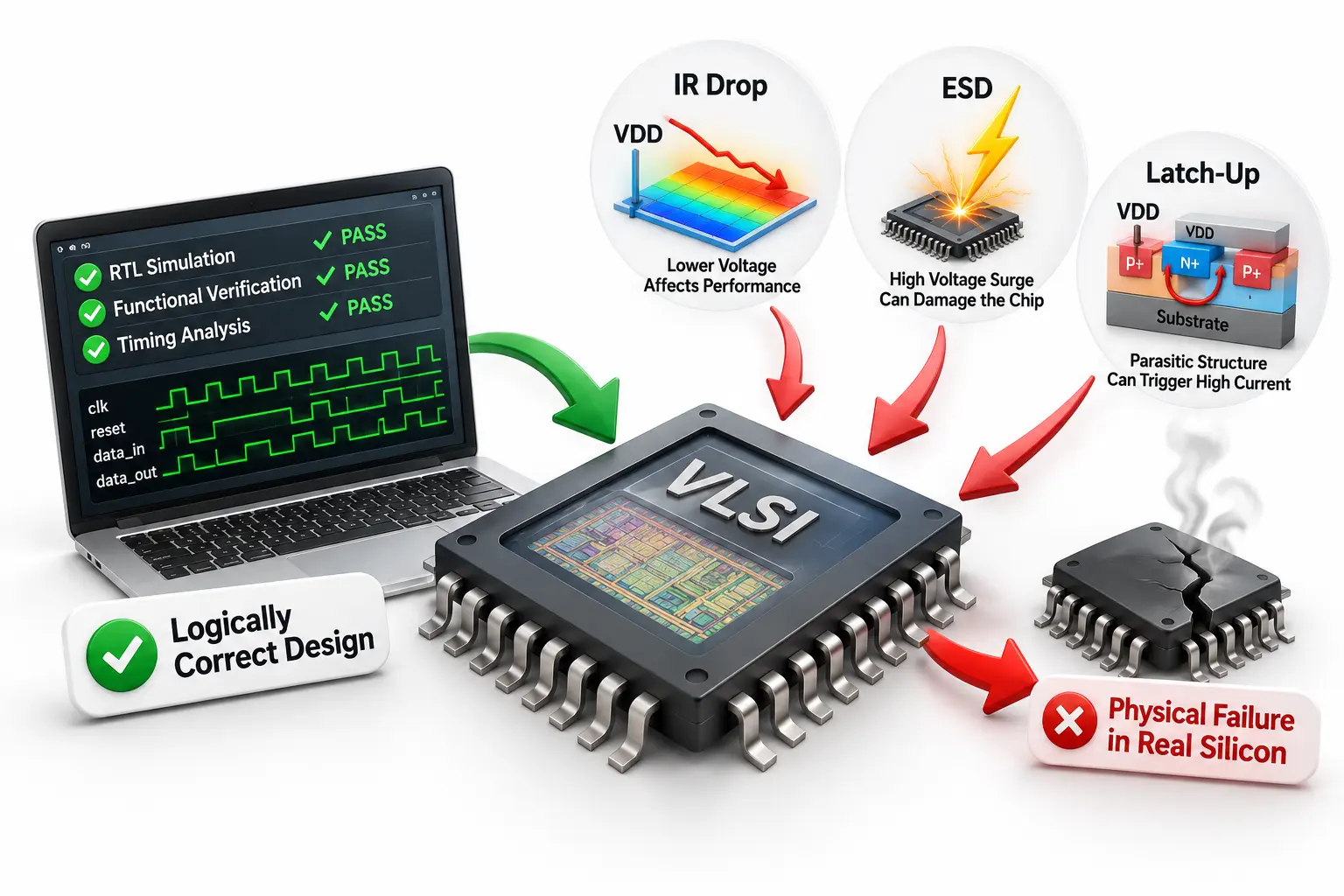
Digital design often encourages engineers to think in clean binary values: a signal is 0 or 1, a clock edge arrives, and a gate changes state. Real silicon is less ideal. Every metal connection has resistance, transistors interact with physical substrate structures, and external pins can experience electrical stresses far beyond normal operating conditions.
That means successful silicon requires several layers of correctness. Functional verification asks whether the design behaves according to specification. Timing analysis checks whether signals arrive within required windows. Physical verification checks whether the manufactured geometry satisfies constraints. Reliability analysis asks another question: will the chip continue working under real electrical conditions?
IR drop, ESD and latch-up illustrate three different failure paths:
IR drop: insufficient local supply voltage because current flows through a resistive power network.
ESD: a short, high-voltage/current electrical event stresses vulnerable devices.
Latch-up: parasitic structures inside CMOS create an unintended low-resistance path between supply rails.
Understanding those differences prevents engineers from treating every silicon failure as simply a logic bug.
See How IR Drop Turns the Power Grid Into a Timing Problem
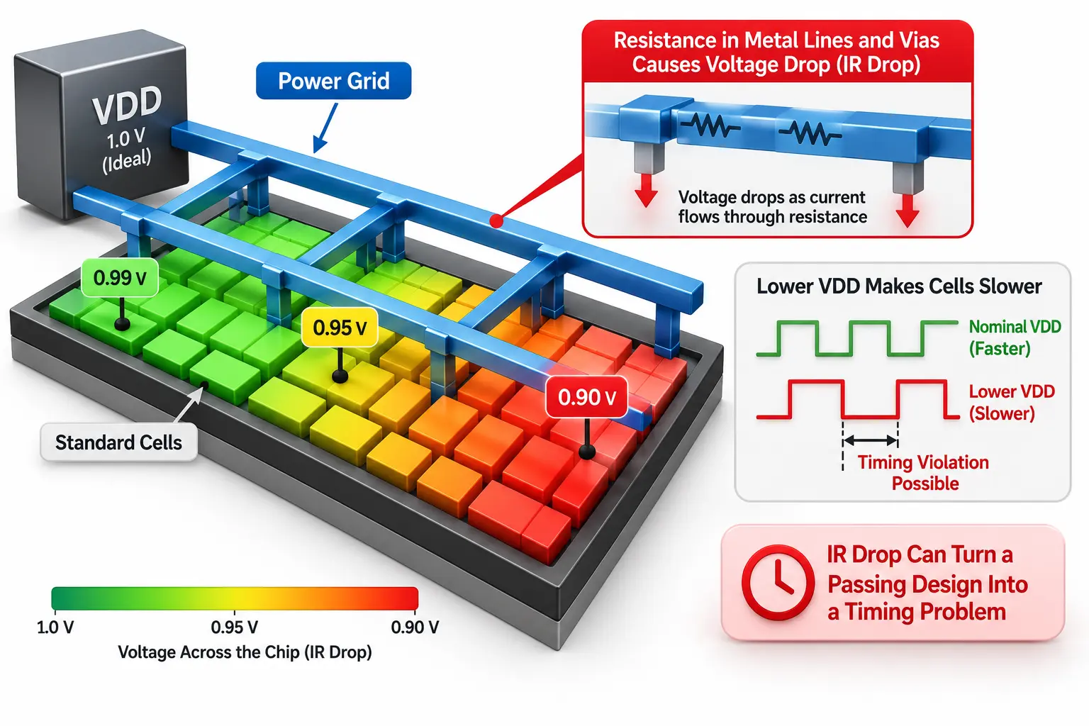
The power distribution network does not deliver perfectly identical VDD everywhere. Metal lines, vias, rails and other conductive structures have finite resistance. When current flows through resistance, voltage is lost according to the familiar relationship V = IR.
Suppose a region expects a nominal supply but receives less because of excessive local voltage drop. Standard cells operating there can become slower. A timing path that looked safe under expected conditions can lose margin, potentially producing setup failures or functional instability.
Engineers commonly distinguish static IR drop, associated with sustained current demand, from dynamic voltage drop, where simultaneous switching produces temporary local supply droop. High switching activity, weak power-grid connectivity and concentrated current demand can make hotspots worse.
Typical mitigation includes:
Wider or additional power straps
More robust via connectivity
Better distribution of high-current cells
Stronger connections around power-hungry macros
Strategic decoupling capacitance for transient demand
Early power-grid planning rather than waiting for final sign-off
This is one reason physical design cannot be reduced to simply placing cells and routing wires. Power delivery directly influences performance.
Learn Why ESD Can Damage a Chip in an Instant
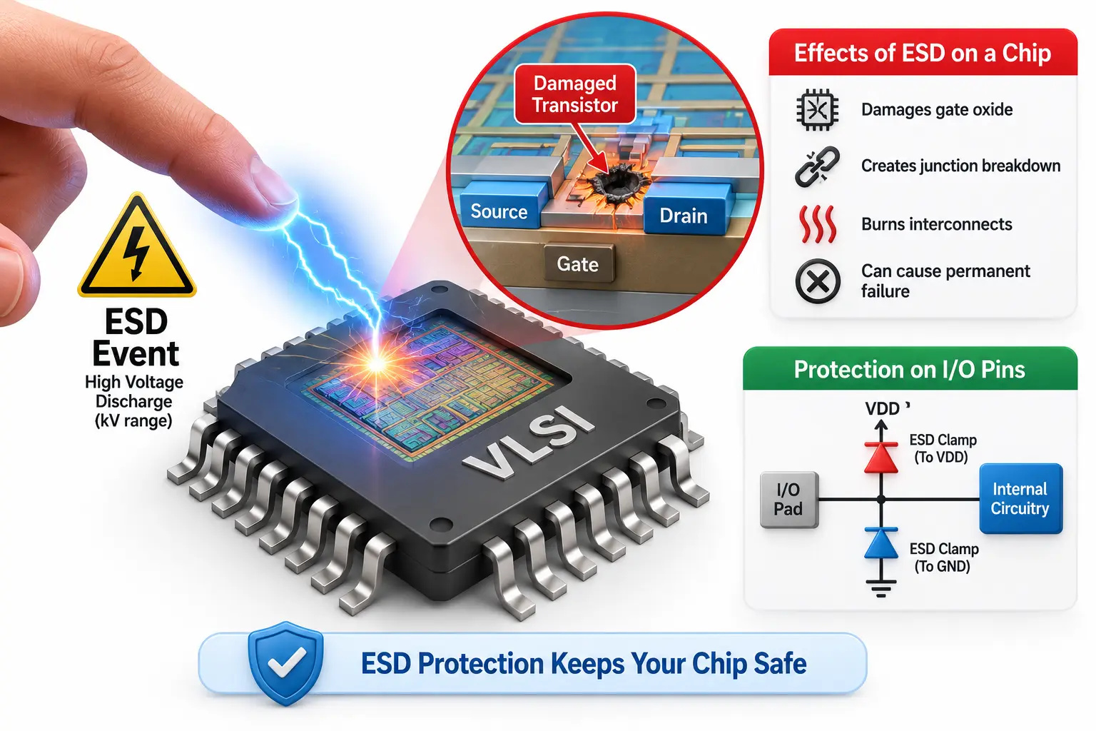
Electrostatic discharge is very different from IR drop. Instead of gradually losing voltage across the PDN, ESD involves a rapid electrical stress event. Charge accumulated on a person, tool, package or other object can discharge through an IC connection and create voltage or current conditions far beyond normal operation.
Modern transistors and interconnect structures are extremely small, making protection essential. Without a suitable discharge path, ESD stress can damage junctions, gate structures, metal connections or other vulnerable structures.
An ESD protection network therefore aims to divert dangerous current away from sensitive internal circuitry. Depending on the technology and interface, protection can involve clamps, diodes and specialized protection devices around I/O and power structures.
A useful conceptual flow is:
ESD event → protection structure activates → current receives a controlled discharge path → internal circuitry experiences reduced stress.
The challenge is that protection cannot be designed independently of everything else. Protection structures add capacitance and occupy silicon area, and their placement and interaction with substrate structures matter. Engineers therefore balance robustness with I/O performance, area and other design constraints.
For students comparing career paths, Which VLSI Domain Should You Choose: RTL, Verification, or Physical Design? becomes easier to answer when they understand these physical effects. Engineers fascinated by power networks, layout geometry, reliability and silicon behavior may find physical design particularly engaging.
Understand How Latch-Up Creates an Unwanted Path Through CMOS
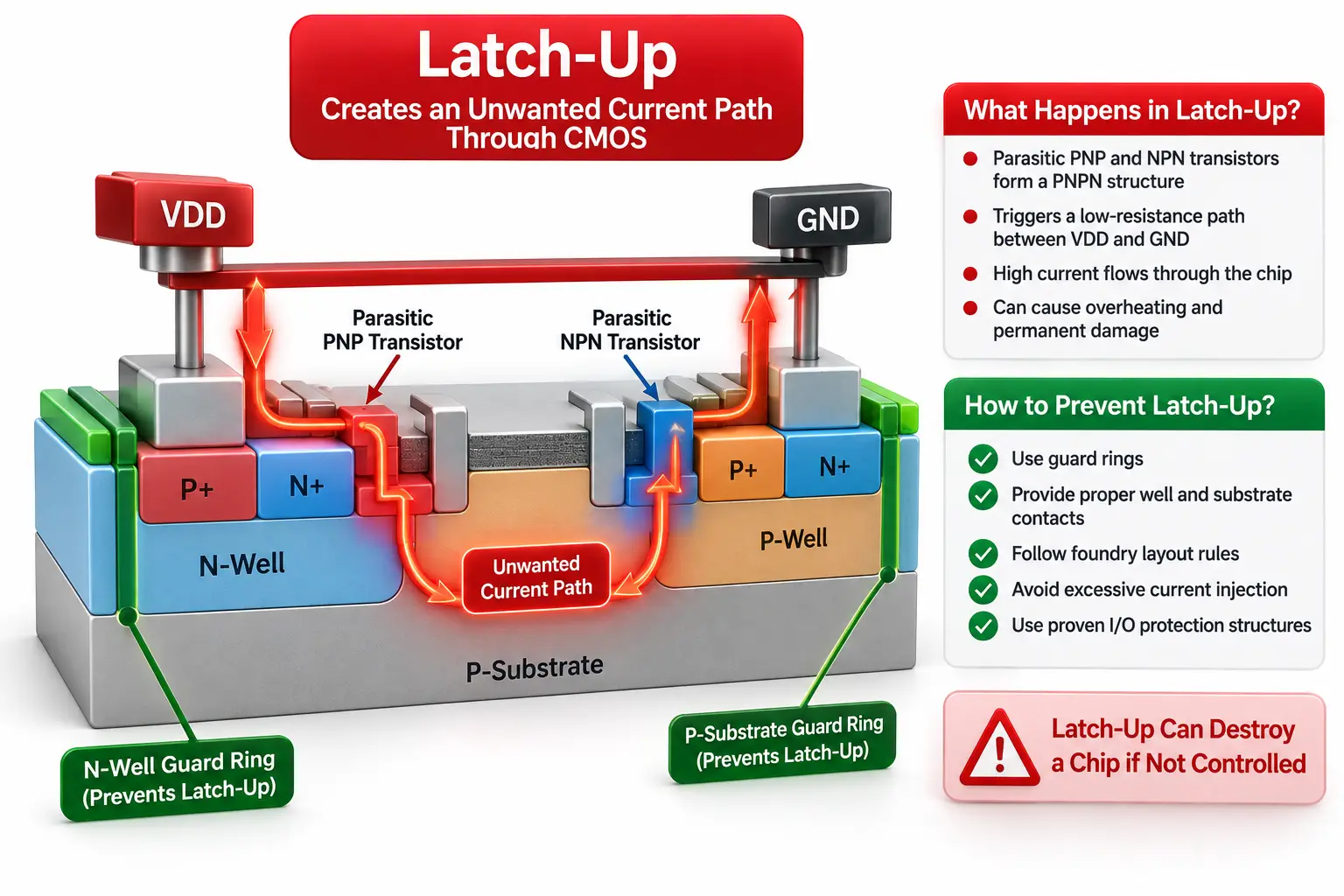
Latch-up is one of the most interesting examples of the difference between a circuit schematic and physical silicon. CMOS fabrication can inherently create parasitic PNP and NPN transistor structures. Under certain conditions, their interaction can behave like a parasitic PNPN structure similar to a silicon-controlled rectifier.
Once triggered, this structure can establish a low-resistance path between VDD and ground. The resulting current may remain high even after the original trigger disappears, potentially causing malfunction, overheating or permanent damage if the condition is not interrupted.
Possible triggers include transient disturbances, current injection and abnormal I/O conditions. That also explains why engineers should not study ESD and latch-up as completely unrelated subjects: electrical events around I/O structures and substrate current injection can influence latch-up susceptibility.
Common preventive approaches include:
Guard rings around sensitive or injecting structures
Appropriate well and substrate contacts
Reduced well/substrate resistance
Correct spacing according to process rules
Careful I/O and protection-device layout
Technology-specific isolation structures
Guard rings are especially important because they can collect injected carriers before those carriers contribute to triggering the unwanted parasitic structure. However, actual implementation must follow foundry rules rather than a universal spacing recipe.
Connect IR Drop, ESD and Latch-Up to Real Physical Design Decisions
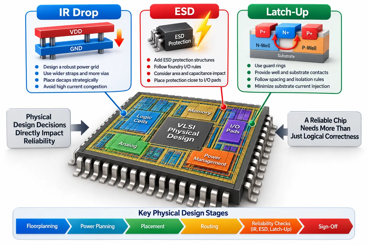
The most valuable lesson is not memorizing three definitions. It is understanding where design choices influence them.
During floorplanning and power planning, engineers need to anticipate current demand and construct a sufficiently robust PDN. Placement can influence local current density. Power straps, metal widths and vias affect resistance. Later analysis identifies weak regions before tape-out.
ESD and latch-up introduce another dimension: device placement, substrate interaction, I/O structures, guard rings and foundry reliability rules. A layout that appears geometrically legal may still require careful reliability engineering.
Think about the distinction this way:
IR drop asks: Can enough voltage reach the circuitry?
ESD asks: Can abnormal electrical energy be safely diverted?
Latch-up asks: Can parasitic silicon structures accidentally create a destructive conduction path?
These questions connect circuit design with the actual physics of manufactured silicon.
For learners searching for a vlsi training institute in india, this distinction matters. Training should move beyond software commands and teach why power integrity, layout structures, sign-off checks and reliability constraints exist. JastTech can use such practical, mechanism-based learning to help engineers connect theoretical CMOS concepts with industry-oriented VLSI workflows.
Build a Reliability Mindset Before You Reach Sign-Off
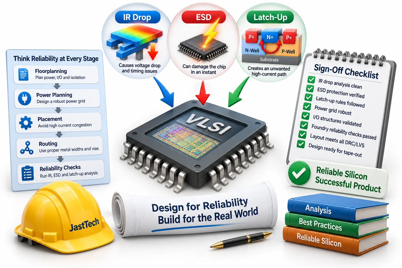
One common mistake is treating reliability as something checked only near tape-out. Late discovery can make problems expensive because fixes may affect placement, routing, timing, congestion or even the power-grid architecture.
IR-drop awareness should therefore begin during floorplanning and PDN development. High-current macros, switching hotspots and weak supply regions can be considered before routing becomes difficult to modify. Detailed analysis later provides the accuracy required for closure rather than becoming the first time power integrity receives attention.
The same engineering mindset applies to ESD and latch-up. Protection structures and isolation requirements must be considered as part of technology and layout planning. Foundry design rules, qualified protection approaches and appropriate verification methodologies matter because semiconductor reliability is highly process-dependent.
A strong engineer consequently learns to ask not only, “Does my design work?” but also:
What happens under worst-case current demand?
What physical path supplies this block?
What happens during abnormal I/O stress?
Could substrate current trigger an unintended structure?
Which checks must pass before this design is safe for fabrication?
That mindset separates tool operation from genuine silicon engineering.
Conclusion
IR drop, ESD and latch-up reveal why VLSI engineering extends far beyond writing RTL. IR drop can reduce effective supply voltage and threaten timing, ESD can expose tiny structures to extreme electrical stress, and latch-up can activate an unintended conduction path inside CMOS silicon. Each failure originates from a different mechanism, yet all demand physical awareness.
As semiconductor systems become denser and more power-conscious, engineers who understand the connection between logic, layout, power delivery and device reliability become increasingly valuable. Learning these mechanisms gives students and working engineers something more important than another definition to memorize: the ability to reason about why real silicon fails and how engineering decisions can prevent it.