


Physical Design Engineer vs. STA Engineer: Responsibilities, Skills, and Career Growth
Navigate through this article using the table of contents below
Table of Contents
No headings found in this article.
Two engineers can sit in the same tapeout review, look at the same chip, and worry about completely different things. One is asking whether every wire and cell will physically fit. The other is asking whether every signal will arrive on time. That gap sits at the center of the physical design engineer vs STA engineer question, and it confuses many people who are just entering VLSI through physical design training.
The two roles overlap more than most job descriptions admit. Understanding where they split, and where they depend on each other, can shape what you learn first and how far you grow.
What a Physical Design Engineer Actually Does
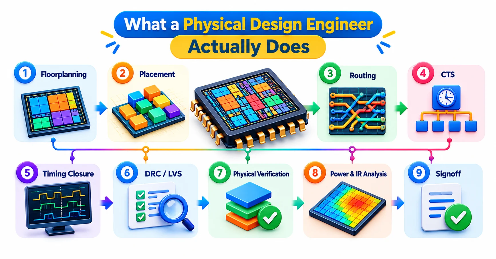
Physical design is the stage where a logical circuit becomes something a foundry can manufacture. The engineer takes a synthesized netlist, which lists the gates and how they connect, and turns it into a placed and routed layout that meets targets for area, power, and speed.
The work follows a rough sequence. Floorplanning decides where large blocks, memories, and I/O sit. Power planning builds the grid that feeds every cell. Placement positions millions of standard cells, clock tree synthesis distributes the clock, and routing draws the metal wires. After that comes a long stretch of fixing: congestion, IR drop, design rule violations, and timing paths that fall short.
A useful picture is a city planner. Streets are limited, buildings need to sit close to the things they talk to, and power lines must reach everywhere. Plan badly and traffic jams appear no matter how clever the buildings are.
Daily work means running tool flows, reading reports, and deciding which knob to turn. A congestion hotspot near a memory macro might be solved by moving the macro, adding placement blockages, or reshaping the floorplan. Each choice affects timing and power, so the job rewards people who think in trade-offs rather than single fixes.
The work ends with physical verification, such as design rule checking and layout versus schematic checks, commonly run in tools like Calibre. A design that is fast but fails these checks cannot be manufactured.
Engineers often specialize later in block-level implementation, top-level integration, clock design, power integrity, or physical verification. Beginners usually start at block level, where the whole flow is visible on a manageable piece of silicon. To see the depth interviewers expect at this stage, this set of physical design interview questions and answers is a practical reference.
What an STA Engineer Does, and Why Timing Is Its Own Discipline
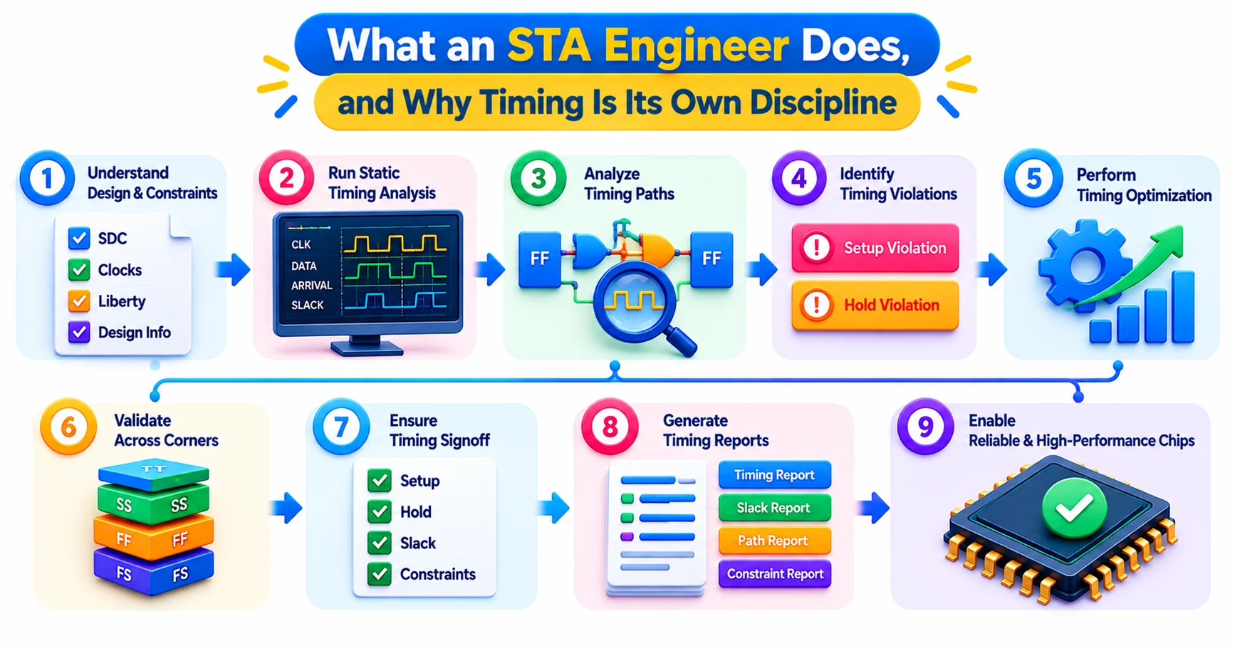
Static timing analysis, or STA, checks whether a design meets its timing requirements without simulating every possible input. Instead of running test patterns, the tool walks through every path between flip-flops and compares signal arrival times against what the clock allows.
Two checks dominate. Setup checks ask whether data arrives before the capturing clock edge. Hold checks ask whether data stays stable long enough after that edge. Slack is the margin on either check, and negative slack means a violation.
An STA engineer owns the correctness of that analysis. This starts with constraints. The SDC file tells the tool what the clocks are, what the input and output delays look like, and which paths can be ignored or given extra cycles. A single wrong false-path exception can hide a real failure, and that kind of mistake can survive all the way to silicon. Many experienced engineers say bad constraints are more dangerous than bad timing.
The second part is signoff. A chip must work across process, voltage, and temperature combinations, often called corners, and across operating modes like functional, scan, and low power. The STA engineer sets up these scenarios, applies variation models such as OCV or POCV, and includes crosstalk effects from neighboring wires. Tools like Synopsys PrimeTime and Cadence Tempus are standard here.
The third part is closing the gaps. When paths fail, the STA engineer works out why. Is the clock skew unfavorable, is a net too long, is a cell too weak, or is the constraint itself wrong? They then suggest or generate timing ECOs, which are small, targeted netlist changes that avoid redoing the whole layout.
The analogy that fits is an auditor. The physical design engineer builds the design, and the STA engineer independently verifies that the numbers add up. Good auditors need strong fundamentals in how digital circuits behave, because they must tell a genuine problem from a tool artifact.
Where the Two Roles Meet During Timing Closure
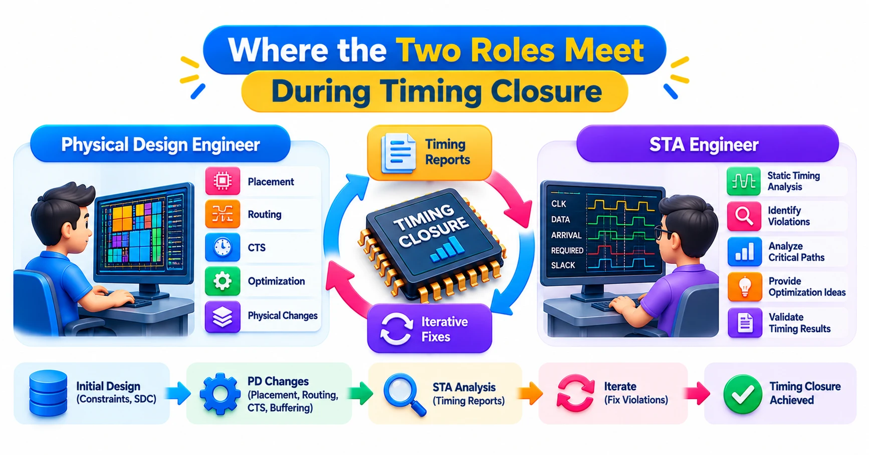
On paper the roles look separate. In a real project they are in constant conversation, and timing closure is where that shows up most.
Consider a hypothetical block with a few hundred failing setup paths after routing. The physical design engineer sees them as layout problems and the STA engineer sees them as analysis results. They need both views to solve it.
The STA engineer first checks whether the failures are real. Perhaps the paths cross a clock domain boundary that should have been marked as an exception, or the constraint file was updated but the layout flow still uses the older version. If the violations are genuine, the next question is the pattern. A cluster of failures through one macro suggests a placement or floorplan issue. Scattered failures with high wire delay suggest routing detours. Failures with large clock skew point back to clock tree synthesis.
The physical design engineer then picks the fix. Options include cell sizing, buffer insertion, swapping to faster threshold voltage cells, adjusting placement, or reworking routing layers for critical nets. Faster cells cost leakage power, and wider spacing costs area, so each fix must be weighed against other goals.
Then the loop repeats. The STA engineer reruns analysis, finds the next set of paths, and flags any new hold violations that the setup fixes created. This back-and-forth can run for many iterations before the design converges.
Two beginner mistakes show up often here. The first is treating timing as someone else’s problem, which leads to layouts that need heavy rework. The second is trusting the tool output without questioning the constraints behind it. Physical design engineers who understand STA write better layouts, and STA engineers who understand physical design give more useful feedback. In smaller companies, one person frequently does both jobs, which is worth knowing when you read job postings.
Skills and Tools: Where the Toolkits Differ
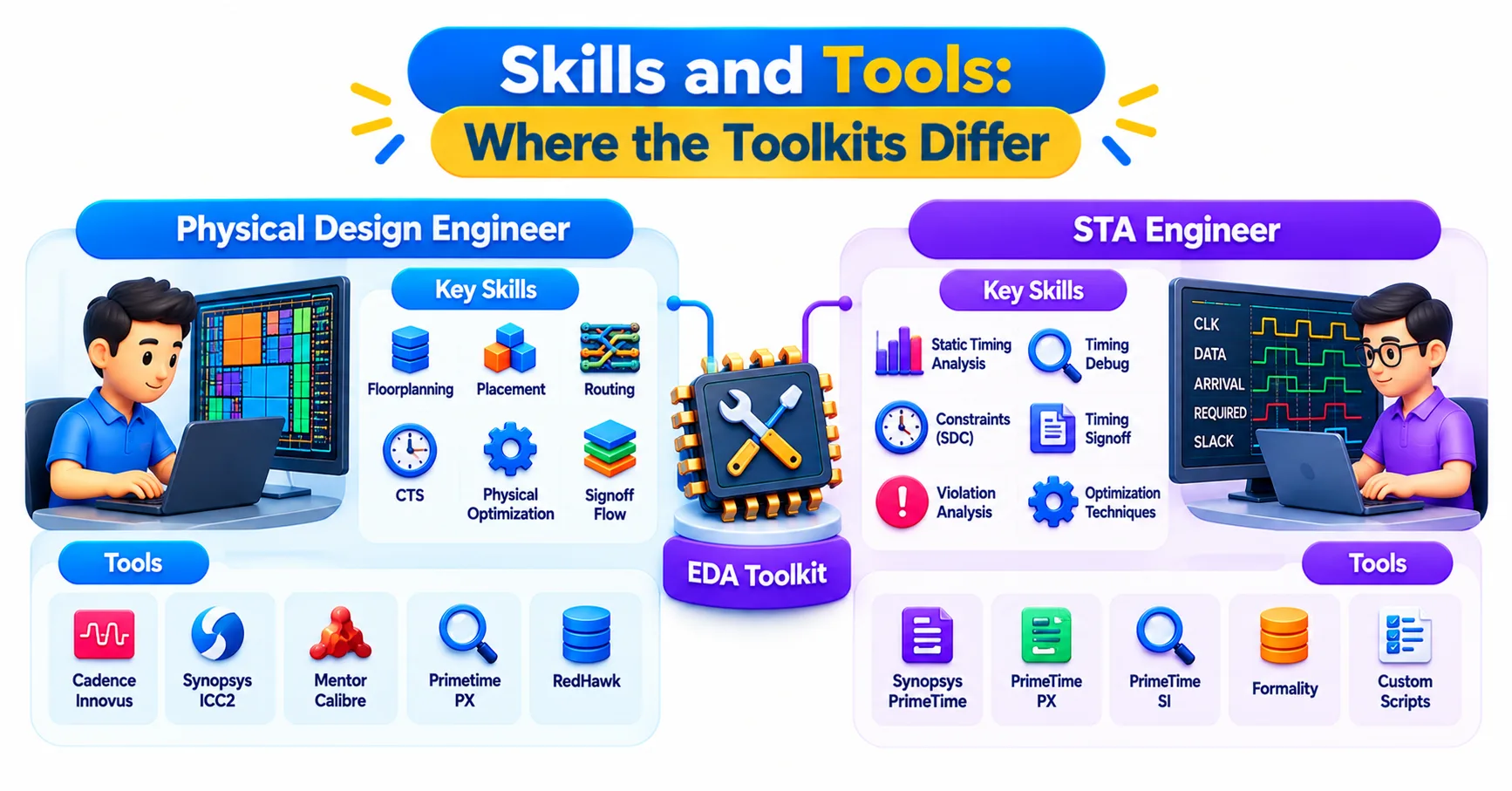
The two roles share a foundation. Both need solid digital design basics, a working picture of CMOS behavior, and comfort with the standard ASIC flow from RTL to GDSII. Both rely on scripting, mainly Tcl, with Python and Perl widely used for reports and automation.
Beyond that, the emphasis shifts.
A physical design engineer typically needs:
Strong understanding of floorplanning, placement, clock tree synthesis, and routing
Familiarity with place-and-route tools such as Cadence Innovus or Synopsys IC Compiler II and Fusion Compiler
Knowledge of power delivery, IR drop, and electromigration
Awareness of design rules and how they change at advanced nodes
Spatial and trade-off thinking, because most problems have more than one fix
An STA engineer typically needs:
Deep command of setup and hold analysis, clock uncertainty, skew, and latency
Fluency in SDC, including exceptions like false paths and multicycle paths
Understanding of Liberty timing models, parasitic extraction formats such as SPEF, and variation models
Experience with multi-corner, multi-mode analysis
Careful, detail-oriented habits, since one missed exception can matter
The mindset also differs. Physical design is a creative and iterative craft where you produce something and then improve it. STA is closer to investigation, where you question assumptions and prove that the design is safe. People who enjoy hands-on building often lean toward physical design, while those who enjoy digging into root causes often find STA more satisfying.
One practical point: STA knowledge is not optional for physical design engineers. You cannot fix timing violations you cannot read. If you are starting out, learn STA concepts alongside the physical design flow rather than after it. JastTech’s training approach follows this idea, treating timing as part of the flow rather than a separate subject.
Physical Design Engineer vs STA Engineer: Which Career Path Fits You?

Both paths are respected and both lead to senior technical roles, but they grow in different directions.
Physical design careers tend to broaden over time. A junior engineer handles a block, a senior engineer owns a larger partition, and a lead manages top-level integration and the schedule to tapeout. From there, people move into physical design management, methodology and flow development, or specialist areas like advanced node implementation and low-power design. Because the role touches so many stages, it also opens doors to related areas such as CAD and EDA flow engineering.
STA careers tend to deepen. A junior engineer runs analysis and reviews reports. A senior engineer owns constraints for a full chip, defines signoff methodology, and decides what margins are acceptable. These engineers often become the final authority on whether a chip is ready to tape out, which carries real responsibility. Some move into timing methodology, library characterization, or design closure leadership.
Job titles vary between companies, and that matters. Some organizations have dedicated signoff or STA teams. Others fold timing into physical design, so a single engineer implements the layout and closes timing. Larger semiconductor and design services firms are more likely to separate the roles, while smaller teams often combine them. Read the actual responsibilities in a job description rather than the title.
A few questions can help you decide:
Do you prefer building and optimizing, or analyzing and verifying?
Are you comfortable owning a decision where a mistake is expensive and hard to see?
Do you want a broad view of the whole chip flow, or deep expertise in one critical area?
There is no wrong answer, and the choice is rarely permanent. Many engineers begin in physical design, develop strong timing skills, and later move into dedicated STA work, or the reverse. Entry points are usually through physical design, since it offers more openings for freshers, and timing expertise then grows from within the role.
How to Prepare and Choose Your Starting Point

If you are unsure which role to aim for, start with the foundation they share rather than picking a side too early.
First, get the fundamentals right. Review digital electronics, flip-flop timing, setup and hold concepts, and basic CMOS behavior. These topics appear in interviews for both roles, and weak fundamentals show quickly.
Second, learn the full flow at a conceptual level. Understand what happens from synthesis through floorplan, placement, clock tree, routing, and signoff. You do not need every tool at first, but you should know what each stage produces and why it matters.
Third, build hands-on practice. Work through a small block on an open or academic flow if you can, or through guided lab exercises in a structured course. Reading a timing report and tracing a failing path teaches more than reading about it. Try to explain, in your own words, why a particular path failed and what you would change.
Fourth, practice the questions interviewers actually ask. Expect conceptual questions on clock skew, on-chip variation, congestion, and ECOs, along with scenario questions such as what you would do if hold violations appeared after routing. Working through realistic VLSI physical design interview questions helps you find the gaps before an interviewer does.
Finally, pick a direction based on how your first projects feel. If you enjoy watching a messy floorplan become clean and routable, physical design is likely a good fit. If you find yourself drawn to tracing why a single path misses by a few picoseconds, STA may suit you better. Either way, learning both sides makes you more employable and more useful on a real team.
Conclusion
The physical design engineer vs STA engineer comparison comes down to building versus proving. One shapes the layout, the other verifies that it works. Each role makes the other better, and the engineers who grow fastest understand both. Choose the starting point that matches how you like to solve problems, then keep learning the other half.