

What Is the Difference Between a Latch and a Flip-Flop in VLSI?
Navigate through this article using the table of contents below
Table of Contents
No headings found in this article.
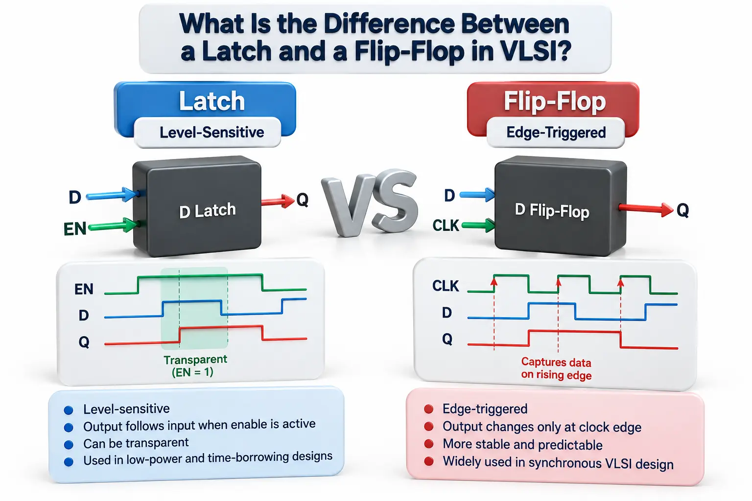
A latch and a flip-flop can both store exactly one bit, so why does VLSI design treat them so differently? The answer is not simply that one uses a level and the other uses an edge. That small timing distinction changes when data can move, how timing paths behave, and how engineers design reliable digital systems.
For a beginner, latch vs flip-flop may look like another digital-electronics comparison to memorize. In an actual VLSI workflow, however, the difference affects RTL coding, synthesis, static timing analysis, power, performance, and even whether a storage element was intentionally created in the first place.
Start With What Latches and Flip-Flops Actually Store
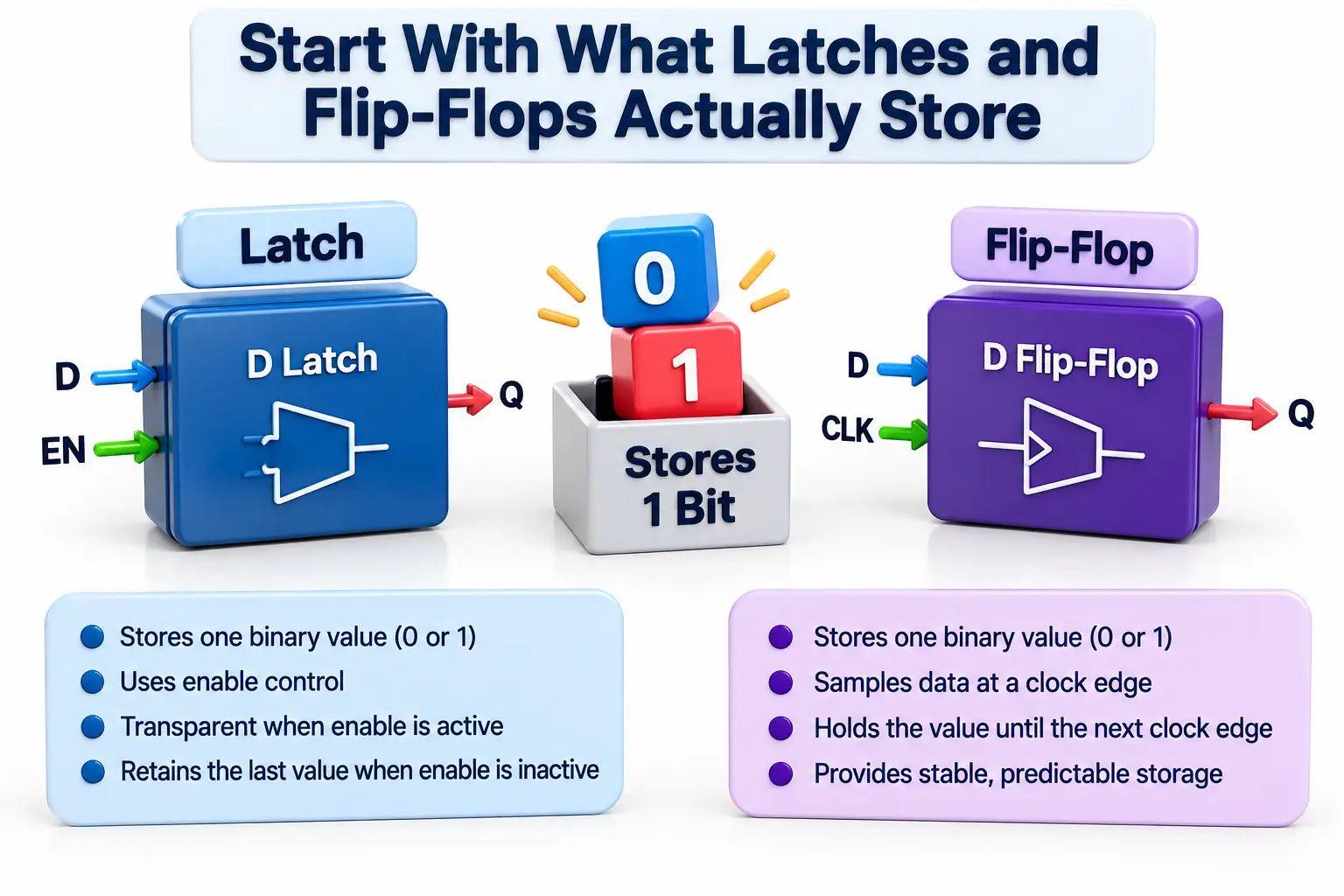
Both latches and flip-flops are sequential storage elements capable of retaining one binary value. Unlike combinational logic, where the output is determined by current inputs, sequential logic contains state. That stored state allows digital systems to create registers, counters, pipelines, finite-state machines, control logic, and many other structures.
A D latch typically has a data input D, an enable or gate control, and output Q. When its enable is active, the latch is transparent. During this interval, changes at D can propagate to Q after the circuit's propagation delay. When enable becomes inactive, the latch closes and retains the last accepted value.
A D flip-flop behaves differently. Its output does not continuously follow D during an active clock level. Instead, it samples data around a particular clock transition, normally a rising or falling edge, and then holds that captured state until another active edge.
The essential idea is therefore:
Latch: level-sensitive storage
Flip-flop: edge-triggered storage
Both: capable of storing one bit
Major difference: when they are allowed to capture data
That final point is where the VLSI implications begin.
Understand Why Level-Sensitive and Edge-Triggered Are Not the Same
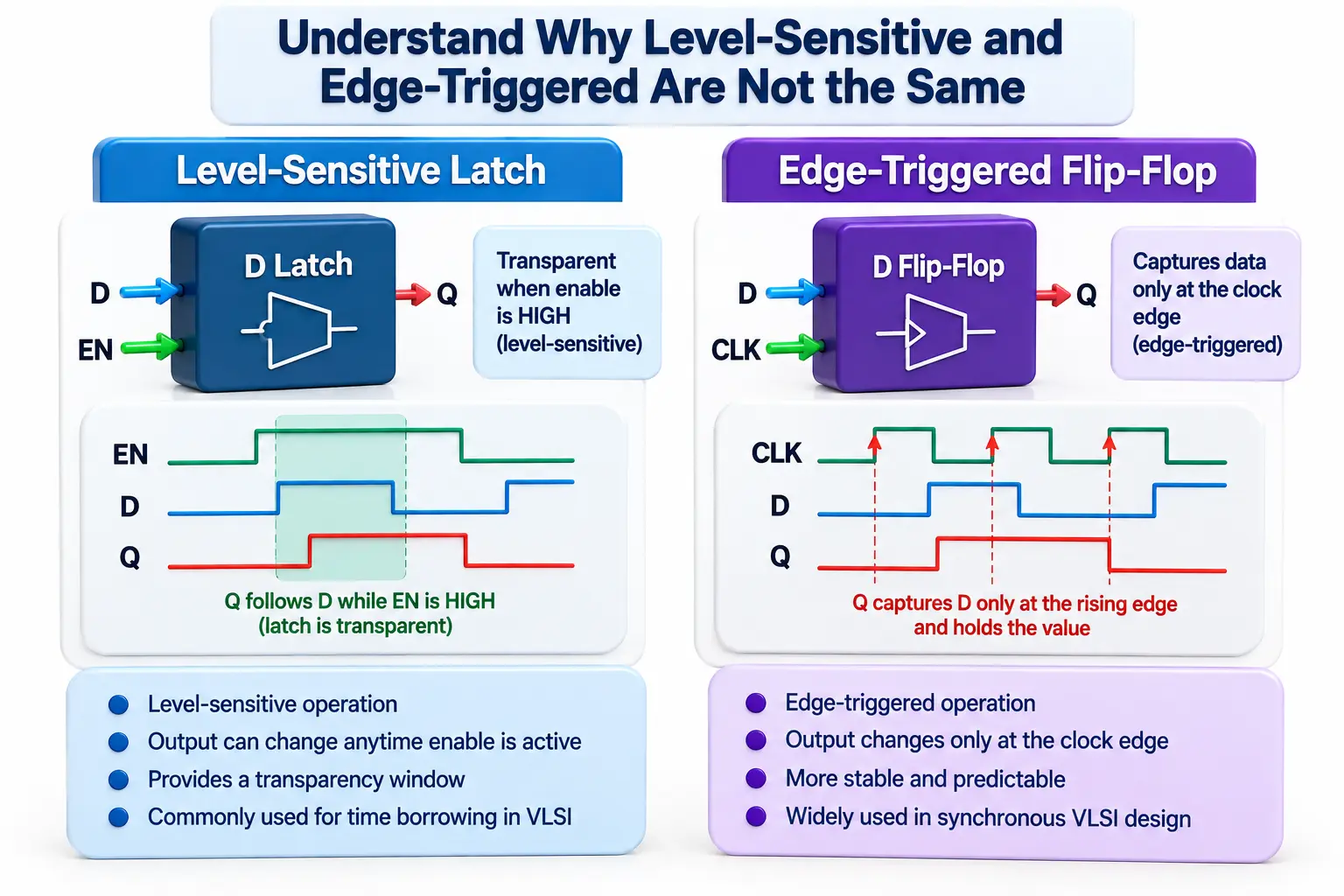
Imagine a positive-level D latch controlled by a clock. While the clock is LOW, the latch is closed and Q retains its previous state. When the clock becomes HIGH, the latch opens. During that HIGH interval, input data can potentially propagate through the latch. When the clock returns LOW, the latch closes and stores the final valid value.
A positive-edge-triggered D flip-flop provides a much narrower sampling event. It captures the input around the LOW-to-HIGH transition. Once that transition has passed, changes at D do not normally affect Q until the next active clock edge.
Consider data changing several times while the clock remains HIGH. A transparent positive-level latch may allow those changes to influence Q. A positive-edge-triggered flip-flop captures the appropriate value at its active edge and isolates subsequent input changes until the next sampling event.
This creates an important mental model: a latch provides a timing window, while a flip-flop provides a timing event.
That distinction is far more useful than simply memorizing “level versus edge,” because it explains why the two storage elements behave differently inside real timing paths.
See How the Difference Changes Timing in a VLSI Design
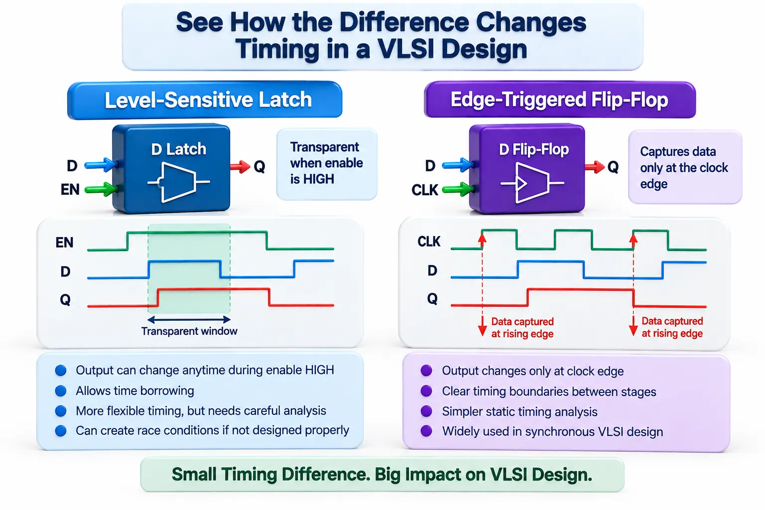
Setup and hold timing are fundamental to both storage approaches. Data must satisfy the timing requirements of the receiving element so that the intended value can be captured reliably. With flip-flop-based synchronous design, engineers commonly analyze paths from one active clock edge to another, which creates relatively clear timing boundaries.
Latch-based timing can be more flexible. Because a latch remains transparent during part of the clock cycle, a signal can sometimes arrive later than a conventional fixed boundary and still pass through before the latch closes. This technique is known as time borrowing.
Suppose one logic stage requires slightly more time while a following stage requires less. A carefully designed latch-based pipeline can allow the slower stage to borrow some timing margin from the next phase. This flexibility can be valuable in high-performance designs.
However, it comes with additional complexity. Engineers must understand:
Latch opening and closing times
Clock phases and non-overlap requirements
Setup and hold constraints
Race conditions
Time borrowing
Minimum and maximum path delays
Static timing analysis across transparent elements
This is why professional learning at a VLSI Training Institute in India should go beyond definitions and connect storage elements with RTL, synthesis, waveforms, and timing analysis.
Learn Why RTL Can Accidentally Create a Latch
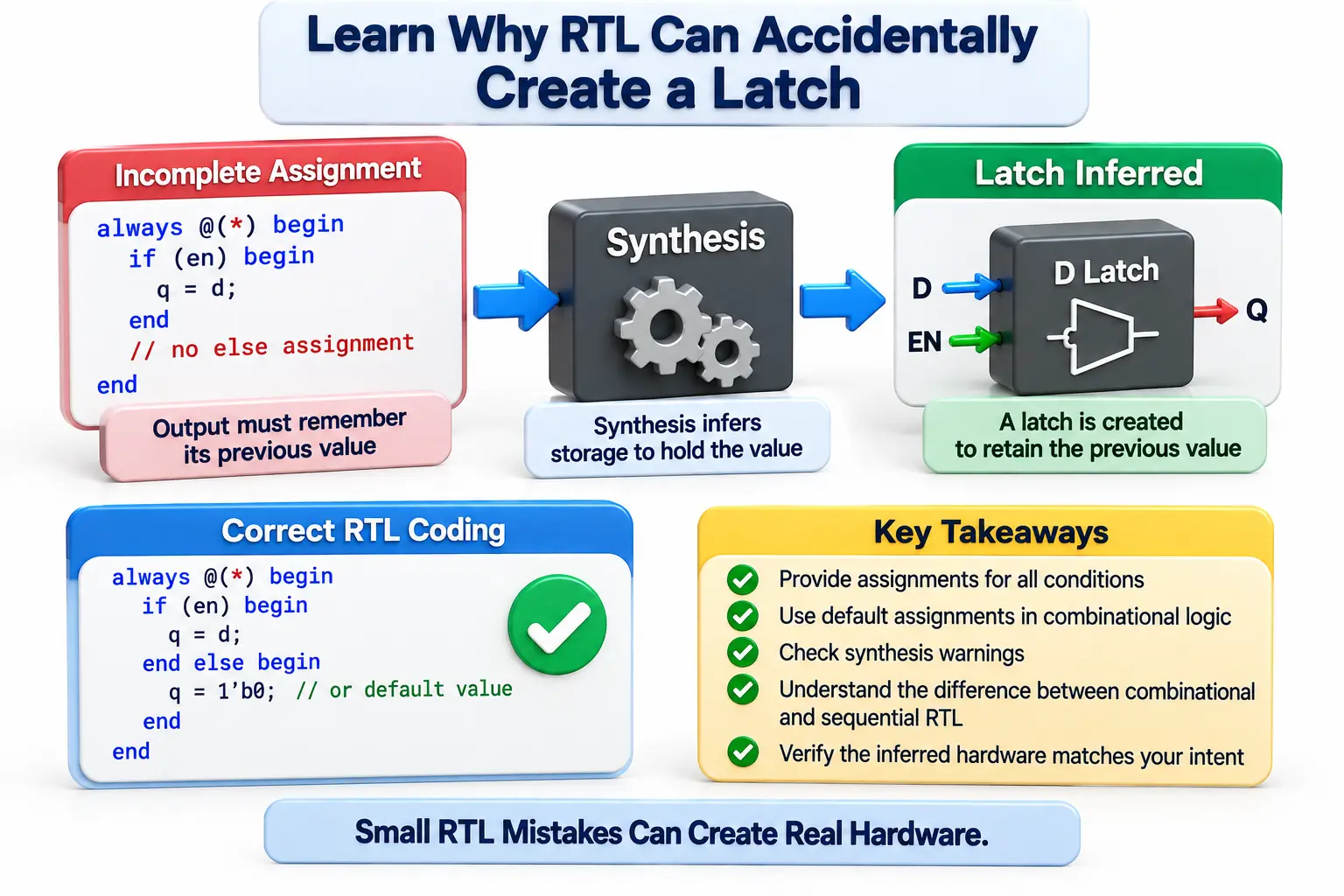
One of the most practical reasons to understand latches is that RTL code can infer one even when the designer never intended to create storage.
Consider combinational logic where an output is assigned only under one condition. If the condition is false and no alternative assignment exists, the circuit needs to remember the previous output value. Synthesis may therefore infer a latch to preserve that value.
Conceptually, problematic logic looks like this:
if (enable) q = d;
If this is intended to describe combinational logic but q receives no assignment when enable is false, the old value must somehow be retained. That requirement for memory can result in latch inference.
Designers can prevent unintended latches by:
Providing assignments for every required branch
Using appropriate default assignments
Reviewing synthesis warnings
Understanding combinational and sequential RTL coding styles
Checking whether inferred hardware matches design intent
The key word is unintended. A latch is not inherently an error. Intentional latch-based architectures exist and can provide useful timing and implementation advantages. The real problem occurs when the synthesized circuit contains storage that the RTL designer did not realize was being created.
Discover Why Flip-Flops Dominate Conventional Synchronous RTL
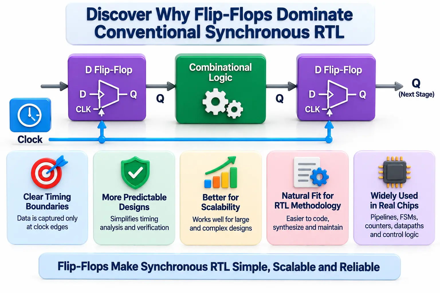
Flip-flops are extremely common in synchronous digital design because edge-triggered behavior creates clear boundaries between pipeline stages. Designers can reason about data being launched by one register, travelling through combinational logic, and being captured by another register at a subsequent active clock edge.
This regular structure works naturally with RTL methodologies, synthesis, clocked pipelines, and static timing analysis. It also makes large designs easier to partition and understand. Registers can separate complex combinational paths into stages while the clock coordinates state transitions across the system.
Flip-flops are commonly found in:
Pipeline registers
Finite-state machines
Counters
Shift registers
Control paths
Datapath registers
Synchronizer structures
Latches can offer benefits such as time borrowing and potentially different power, area, or timing characteristics depending on the implementation. But their transparency requires careful control of timing and clocking. Therefore, engineers should not think of the decision as “flip-flop good, latch bad.” It is an architectural and implementation choice.
At JastTech, understanding this distinction as an engineering decision rather than a memorized interview answer can help learners build stronger foundations for RTL design, verification, synthesis, and timing analysis.
Choose Between a Latch and Flip-Flop by Thinking Like a VLSI Engineer

When asked about latch vs flip-flop in an interview, saying “a latch is level-sensitive and a flip-flop is edge-triggered” is technically useful, but it is only the beginning. A stronger answer explains what this means for the circuit.
A latch can remain transparent throughout its active level. A flip-flop samples at an active clock edge. Therefore, latch-based systems can provide timing flexibility through time borrowing, while flip-flop-based systems provide well-defined sampling boundaries that simplify conventional synchronous design.
A VLSI engineer should also connect the concept to RTL. If a latch appears unexpectedly after synthesis, the engineer should inspect whether a combinational block has incomplete assignments. If a latch is intentional, its transparency window, setup and hold requirements, clocking strategy, and timing paths must all be understood.
For interviews and practical design work, remember the concept in this sequence:
Identify how the storage element captures data.
Understand when its output can change.
Check setup and hold requirements.
Consider transparency and timing paths.
Determine whether the storage was intentionally inferred.
Verify that synthesis and STA behavior match the architecture.
That approach transforms a basic digital-electronics question into actual VLSI engineering reasoning.
Conclusion
The difference between a latch and a flip-flop is fundamentally about when data is captured. A latch is level-sensitive and can remain transparent during an active control level, whereas a flip-flop is edge-triggered and samples data around a specific clock transition. That difference influences timing boundaries, transparency, time borrowing, RTL inference, and implementation strategy.
For aspiring VLSI engineers, memorizing definitions is not enough. Learn to predict waveforms, identify unintended latch inference, understand setup and hold constraints, and explain why an architecture uses a particular storage element. Once you can connect RTL code to the hardware and timing behavior it creates, latch vs flip-flop becomes an engineering concept rather than an interview question.