

Why Hyderabad Is the Best City to Start Your VLSI Career in 2026
Navigate through this article using the table of contents below
Table of Contents
No headings found in this article.
Hyderabad has built a semiconductor ecosystem so strong that engineers who are starting their VLSI careers here are not settling for a backup option — they are choosing the fastest-growing chip design city in South India.
This blog is written specifically for students and freshers in and around Hyderabad. It covers why this city now competes directly with Bangalore for VLSI jobs, which areas in Hyderabad are the real semiconductor hubs, what skills and training are needed to get hired, what salaries look like in 2026, and how to build a career that starts here and grows globally.
Hyderabad's Semiconductor Ecosystem in 2026: What Has Actually Been Built Here
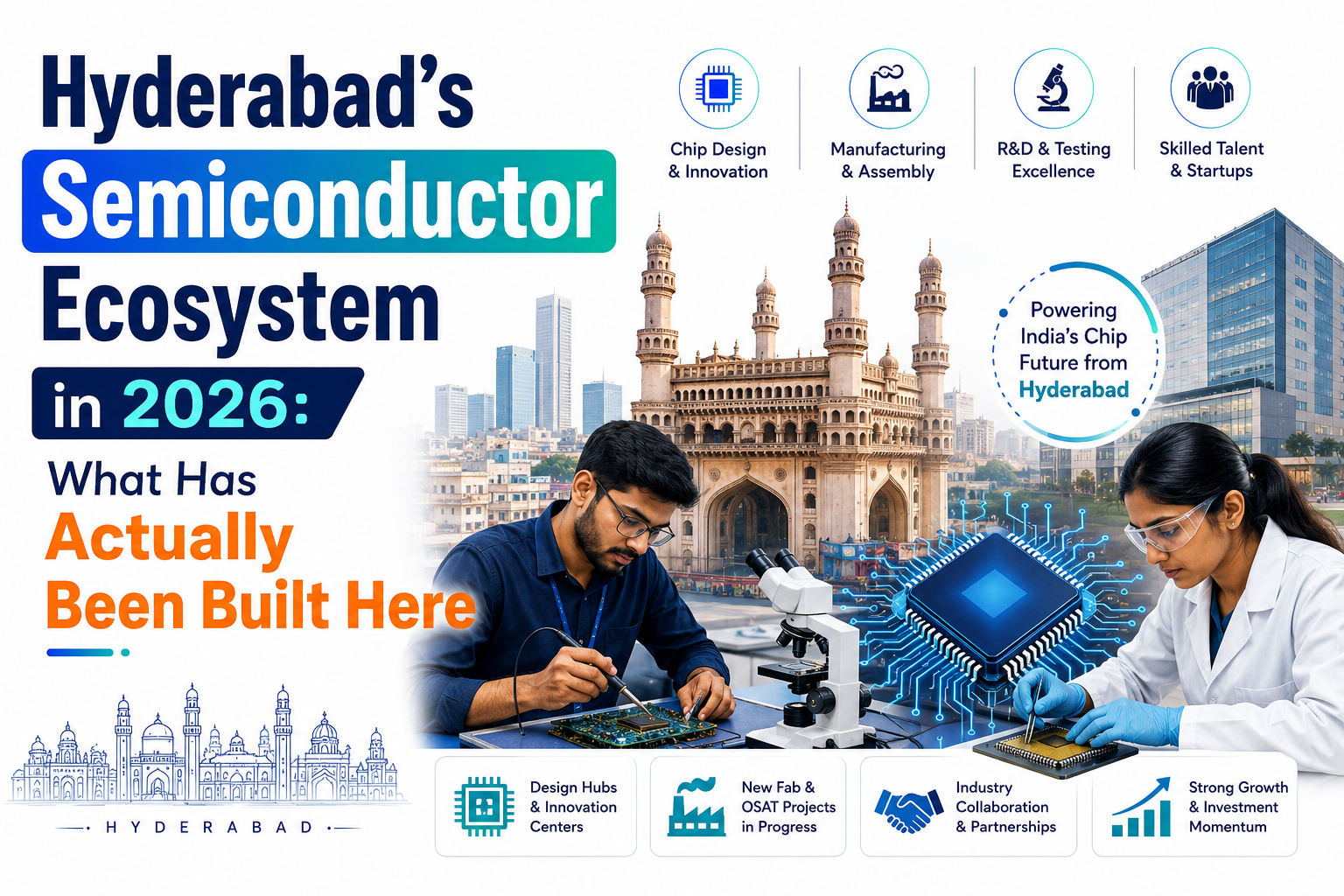
Hyderabad's transformation into a serious chip design city has been driven by real investment, not just headlines. The combination of the Telangana Electronics Policy, HITEC City's world-class IT infrastructure, and a dense pool of engineering graduates from Osmania University, JNTU Hyderabad, BITS Pilani Hyderabad, IIT Hyderabad, and dozens of private colleges has made this city genuinely attractive for global semiconductor companies.
Qualcomm's Hyderabad center, located in HITEC City, is one of the company's largest engineering operations outside the United States. The team here works on Snapdragon processor architecture, 5G modem design, AI engine development, and advanced low-power design — the kind of deep, high-complexity chip work that most engineers outside Silicon Valley never get to touch. AMD's Hyderabad campus, also in the HITEC City corridor, contributes directly to Ryzen and EPYC CPU development and has been expanding its engineering headcount consistently over the past three years.
Apple operates a silicon design team in Hyderabad focused on custom chip development — one of the most exclusive semiconductor R&D operations in India. Intel's Hyderabad center works on FPGA design, SoC development, and silicon validation. Micron Technology has a significant testing and validation presence connected to its broader India operations. NVIDIA, NXP, Cadence, Synopsys, Samsung Semiconductor, and MosChip — India's first fabless semiconductor company, headquartered right here in Hyderabad — round out an ecosystem that spans design, verification, validation, EDA tools, and manufacturing support.
What Skills Hyderabad Semiconductor Companies Actually Hire For

Knowing that Qualcomm and AMD are in Hyderabad is useful. Knowing exactly what skills their hiring teams look for — track by track — is what determines whether you get an interview. Here is what the Hyderabad semiconductor market is actively hiring for in 2026, based on what these companies are building.
RTL Design and Verification — The Highest-Volume Hiring Track in Hyderabad
RTL design and verification is the skill set that Hyderabad needs more of than anything else right now, and the reason ties directly to what Qualcomm and AMD are doing here. Both companies are building large, complex SoCs — chips that combine a processor, a GPU, a modem, an AI engine, and dozens of other blocks in one piece of silicon. Each of those blocks needs to be coded in RTL (Register Transfer Level) and verified rigorously before the whole chip can be assembled.
RTL Design means writing code — using Verilog or SystemVerilog — that tells a chip exactly what to do. It is hardware programming: you are not writing software for a processor, you are describing the hardware itself. Verification means building tests to confirm that the RTL code is correct, using a methodology called UVM (Universal Verification Methodology) that gives verification engineers a structured, repeatable way to stress-test a design across thousands of scenarios before manufacturing begins.
For freshers targeting Hyderabad, RTL design and verification training that includes real hands-on simulation on tools like Synopsys VCS or Cadence Xcelium, UVM testbench development from scratch, and a complete project they built themselves — not followed from a tutorial — is what gets callbacks from Qualcomm, AMD, and Intel recruiters here. JastTech's RTL design and verification training in Hyderabad is structured around exactly this kind of industry-ready, project-first approach, with ISO 9001:2015 certified curriculum and hands-on lab access.
Post-Silicon Validation — Hyderabad's Fastest-Growing and Most Underserved Track
Post-silicon validation is the process of testing a chip after it has been physically manufactured. While simulation-based verification tests a design in theory, post-silicon validation tests the real chip in the real world — with real voltage levels, real temperature variation, real signal noise, and real timing behavior that simulation cannot fully predict.
Intel, Micron, and Qualcomm in Hyderabad all have active post-silicon validation teams, and this is the track where the gap between supply and demand is widest. Most ECE graduates in Hyderabad have never heard of post-silicon validation as a career track, let alone trained for it — which means the competition for these roles is far lower than for physical design or verification, while the salaries are higher than most freshers expect.
Post-silicon validation training needs to cover silicon bring-up, JTAG-based debug access, scan chain usage for internal state visibility, lab instrument operation (oscilloscopes, protocol analyzers, logic analyzers), high-speed interface testing such as PCIe, DDR, and USB, and Python scripting for test automation. It is a broader skill set than most single-track programs, but that breadth is precisely what makes trained validation engineers difficult to find and well-compensated when they are. JastTech offers post-silicon validation training as a dedicated track — one of very few training providers in Hyderabad that does.
Physical Design — Strong Demand for Backend Engineers in Hyderabad
Physical Design engineers take a verified chip design and turn it into a manufacturable layout — handling floorplanning, placement, clock tree synthesis, routing, and timing sign-off. Companies like Synopsys, Cadence, NXP, and Samsung Semiconductor in Hyderabad hire physical design engineers regularly. The key differentiator in 2026 is not just knowing the steps of the Physical Design flow — it is hands-on experience with real EDA tools like Cadence Innovus or Synopsys ICC2 and the ability to discuss timing closure challenges, congestion resolution, and IR drop mitigation in an interview.
VLSI Salaries in Hyderabad in 2026: Honest, Track-by-Track Numbers

Salary data for VLSI roles in Hyderabad is scattered across forums, LinkedIn posts, and job portals, and most of it is either too optimistic or too outdated. Here is a realistic picture based on 2025-26 hiring patterns at companies operating in the city.
RTL Design Engineers entering at Qualcomm, AMD, or Intel in Hyderabad typically start at ₹8 to ₹14 lakh per year when they have solid training and a defensible project. Engineers with three to five years of experience earn ₹22 to ₹35 lakh. Senior RTL architects at these companies — engineers who own the micro-architecture of a chip block — reach ₹40 to ₹60 lakh.
Verification Engineers at the fresher level in Hyderabad start at ₹7 to ₹12 lakh with strong UVM training. Mid-level engineers with four to six years of experience in constrained-random verification, coverage closure, or emulation earn ₹25 to ₹40 lakh. Formal verification specialists, who are particularly scarce in Hyderabad's market, command ₹35 to ₹50 lakh.
Physical Design Engineers with genuine hands-on tool experience enter at ₹6 to ₹11 lakh in Hyderabad and grow to ₹25 to ₹40 lakh with five or more years of backend experience. DFT Engineers follow a comparable trajectory, at ₹6 to ₹10 lakh entry level and ₹22 to ₹32 lakh with experience.
Post-Silicon Validation Engineers are the highest-paid entry-level track in Hyderabad right now. Freshers with real lab training and validation project experience start at ₹9 to ₹15 lakh — higher than any other VLSI track at the same experience level — because the skill is in short supply. Senior validation engineers with five or more years of experience, particularly those who have worked on high-speed interface validation or silicon bring-up, earn ₹35 to ₹55 lakh in Hyderabad.
How to Actually Get Ready for a VLSI Job in Hyderabad: Five Specific Steps
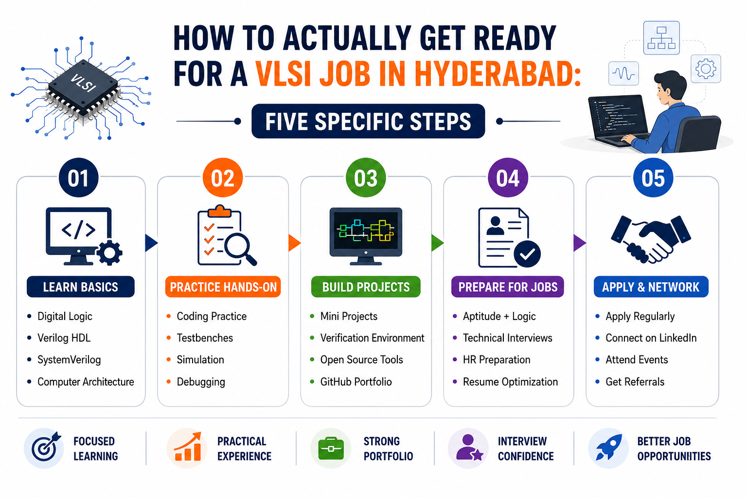
Getting hired at a semiconductor company in Hyderabad is very achievable for freshers in 2026. But the path to getting there is specific — it is not about collecting certificates or watching YouTube tutorials. Here is what actually works.
1. Pick One Track and Build Depth in It, Not Width Across All
Hyderabad's semiconductor hiring market rewards depth over breadth at the fresher level. A candidate who can talk confidently and in detail about RTL design or UVM-based verification for 30 minutes is far more attractive to a Qualcomm or AMD recruiter than a candidate who says they know 'a little bit of Physical Design, some Verification, and a bit of RTL.' Choose one track. Build everything around it.
2. Get Into a Training Program That Gives You Real EDA Tool Access in Hyderabad
Training institutes in Madhapur and Gachibowli vary significantly in tool access. Before joining any program, physically visit the lab and confirm that tools like Synopsys VCS, Cadence Xcelium, Cadence Innovus, or the relevant tool for your track are installed, licensed, and that you will run your own simulations — not watch someone else run them. This single factor matters more than almost anything else for interview readiness.
3. Build One Complete Project You Can Explain Without Notes
The VLSI interview format at Qualcomm, AMD, and Intel in Hyderabad consistently involves a deep technical discussion of your project. One project that you designed from scratch, debugged yourself, and can explain from start to finish — including the design decisions you made and the mistakes you fixed — is worth more than four tutorial projects you followed passively. Make this project a priority from day one of your training.
4. Practice Explaining Concepts Out Loud in Simple English
VLSI interviews at Hyderabad's semiconductor companies test not just what you know, but how clearly you can explain it. Being able to explain clearly what a clock domain crossing is, why setup time matters, or what UVM's scoreboard does — in simple, confident language without reading from a mental script — is a skill that separates hired candidates from rejected ones consistently. Practice this deliberately, ideally with a study group or mentor.
5. Use Hyderabad's Local Network — It Is Closer Than You Think
Because Hyderabad's semiconductor industry is clustered in Madhapur, HITEC City, and Gachibowli, the professional network here is accessible in a way that is genuinely unusual. IEEE Hyderabad Section events, VLSI Society of India meetups, and alumni from training institutes who now work at Qualcomm and AMD hold regular technical sessions. Attending two or three of these while you are training — listening, asking questions, and introducing yourself — builds referral connections that can directly accelerate your interview timeline. Use the geography advantage Hyderabad gives you.
Choosing the Right VLSI Training Institute in Hyderabad: What to Actually Check
Hyderabad has a growing number of VLSI Training Institute but the quality difference between the best and worst options is significant. Here is what to specifically verify before committing.
• Visit the training lab in person before paying: confirm that EDA tools are installed and licensed, that batch sizes are small enough for individual attention, and that you will have lab access outside class hours for practice.
• Ask the trainer directly about their work history: the best VLSI trainers in Hyderabad have worked at semiconductor companies on real chip projects — not just trained students. Ask which company, which chip, and what role. The answer reveals everything.
• Check where recent placed students work: ask for names and LinkedIn profiles of students placed in the last two batches. Verify independently. An institute confident in its placement record will not hesitate.
• Confirm the project structure: your project should be something you build yourself, not a demo the trainer performs. Ask specifically what your project will be and what role you play in building it.
• Choose an institute close to the HITEC City, Madhapur, or Gachibowli belt if possible: proximity to where semiconductor companies actually operate gives you walk-in drive access, networking opportunities, and a faster path from training to interview.
JastTech's Hyderabad center — ISO 9001:2015 certified, covering RTL design and verification, physical design, DFT, and post-silicon validation with hands-on EDA lab access — is positioned to serve students across the HITEC City-Madhapur-Gachibowli corridor and is one of the few training providers in Hyderabad offering post-silicon validation as a dedicated track.
Conclusion
Hyderabad in 2026 is not just a good city for a VLSI career — it is the smartest entry point in South India for freshers who want to get hired faster, build deep skills, and grow within a city that is still expanding its semiconductor base. Qualcomm, AMD, Intel, and Apple are here. The jobs are real, the salaries are strong, and the training infrastructure in Madhapur, Gachibowli, and HITEC City is ready. What is left is your preparation.
\