
Complete Roadmap to Become an RTL Design and Verification Engineer
Navigate through this article using the table of contents below
Table of Contents
No headings found in this article.
What powers the smartphones, laptops, AI accelerators, and advanced electronic devices we use every day? Behind every successful semiconductor chip is a team of skilled RTL Design Engineers who transform complex specifications into efficient digital hardware architectures. As the semiconductor industry continues to grow rapidly with advancements in artificial intelligence, automotive electronics, IoT, and high-performance computing, the demand for RTL Design Engineers has reached an all-time high. For aspiring VLSI professionals, RTL design offers a rewarding career path with excellent growth opportunities, competitive salaries, and exposure to cutting-edge technology.
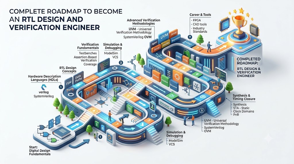
This complete roadmap to become an RTL Design Engineer will guide you through every stage of your learning journey, from understanding digital electronics fundamentals to mastering Verilog, SystemVerilog, FPGA development, ASIC design flow, verification methodologies, and industry-standard EDA tools. Whether you are an engineering student, recent graduate, or working professional looking to enter the VLSI industry, this guide provides a structured learning path to help you build the technical skills, practical experience, and industry knowledge required to secure RTL Design Engineer roles in leading semiconductor companies.
What is RTL Design and Why is it Important in VLSI?
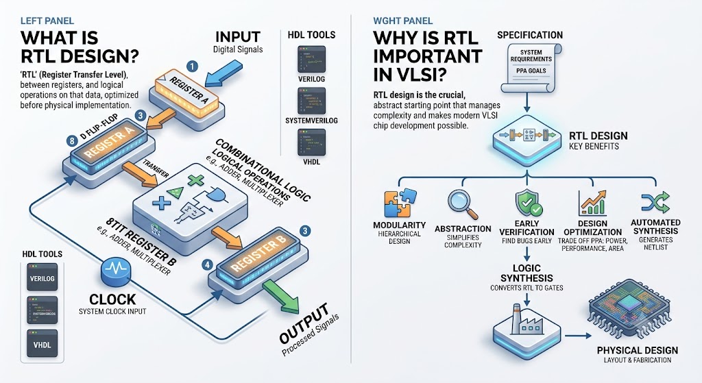
RTL (Register Transfer Level) Design is the process of describing how digital data moves between registers and how logical operations are performed within a hardware system. It serves as a crucial abstraction layer between high-level chip specifications and the physical hardware implementation. RTL design is typically written using Hardware Description Languages (HDLs) such as Verilog and SystemVerilog, allowing engineers to model, simulate, and verify complex digital circuits before fabrication. From simple counters and memory controllers to advanced processors and AI accelerators, every digital integrated circuit begins with a well-structured RTL design.
In the VLSI (Very Large Scale Integration) industry, RTL design plays a fundamental role in transforming system requirements into functional hardware architectures. RTL engineers analyze design specifications, create synthesizable code, optimize performance, and ensure that the design meets power, area, and timing constraints. Since modern semiconductor devices contain billions of transistors, RTL design provides a manageable way to represent complex digital systems while maintaining accuracy and scalability throughout the ASIC and FPGA development process. A robust RTL design forms the foundation for successful synthesis, verification, and physical implementation.
The importance of RTL design in VLSI continues to grow as industries such as artificial intelligence, automotive electronics, 5G communications, consumer electronics, and IoT demand increasingly sophisticated semiconductor solutions. High-quality RTL design helps reduce development costs, minimize design errors, improve chip performance, and accelerate time-to-market. Because every stage of the VLSI design flow depends on a reliable RTL model, skilled RTL Design Engineers are among the most sought-after professionals in the semiconductor industry. Their expertise directly impacts the functionality, efficiency, and success of modern digital products used across the world.
Who is an RTL Design Engineer? Roles and Responsibilities
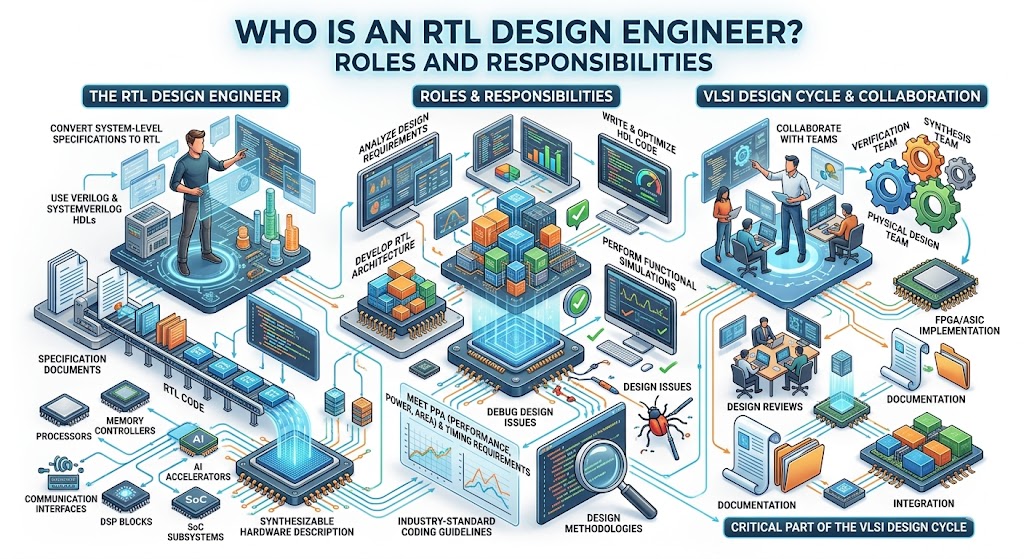
An RTL Design Engineer is a semiconductor professional responsible for designing digital hardware circuits using Register Transfer Level (RTL) methodologies. These engineers convert system-level specifications into synthesizable hardware descriptions using languages such as Verilog and SystemVerilog. Their primary objective is to create efficient, reliable, and high-performance digital designs that can be implemented on ASICs (Application-Specific Integrated Circuits) or FPGAs (Field-Programmable Gate Arrays). RTL Design Engineers work on a wide range of components, including processors, memory controllers, communication interfaces, DSP blocks, AI accelerators, and SoC subsystems, making them a critical part of the VLSI design cycle.
The roles and responsibilities of an RTL Design Engineer include analyzing design requirements, developing RTL architecture, writing and optimizing HDL code, performing functional simulations, debugging design issues, and collaborating with verification, synthesis, and physical design teams. They must ensure that the design meets performance, power, area, and timing requirements while following industry-standard coding guidelines and design methodologies. In addition, RTL Design Engineers participate in design reviews, documentation, and integration activities to ensure seamless development across the chip design flow. Their work serves as the foundation for successful verification, synthesis, and chip implementation, making them indispensable in modern semiconductor product development.
Essential Skills Required to Become an RTL Design Engineer
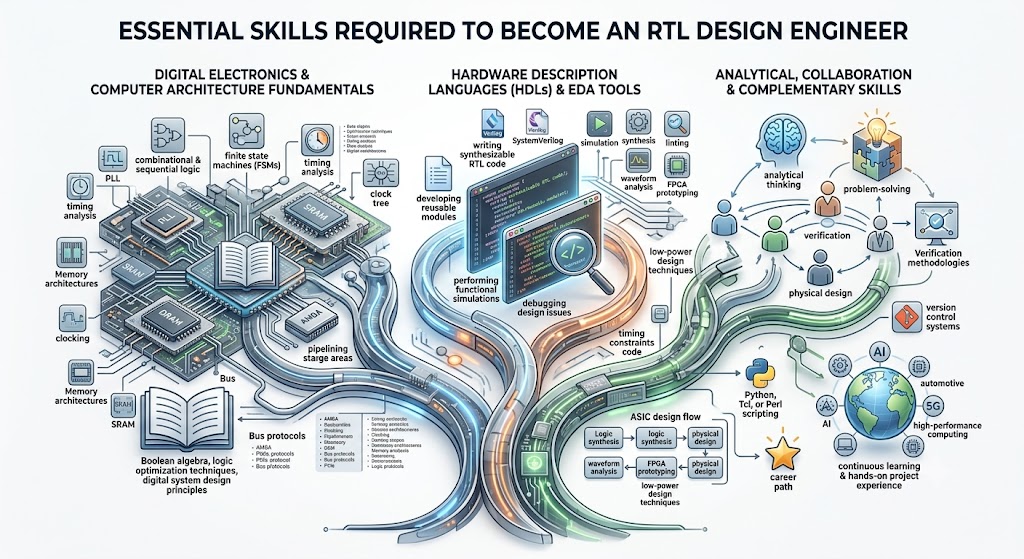
To become a successful RTL Design Engineer, a strong foundation in digital electronics and computer architecture is essential. Engineers must thoroughly understand combinational and sequential logic, finite state machines (FSMs), timing analysis, clocking concepts, pipelining, memory architectures, and bus protocols. These fundamentals help in designing efficient digital circuits and solving complex hardware design challenges. A solid grasp of Boolean algebra, logic optimization techniques, and digital system design principles is equally important, as these concepts form the backbone of modern VLSI design.
Proficiency in Hardware Description Languages (HDLs) such as Verilog and SystemVerilog is another critical skill for RTL Design Engineers. These languages are used to model, simulate, and implement digital hardware at the Register Transfer Level. Engineers should be capable of writing synthesizable RTL code, developing reusable modules, performing functional simulations, and debugging design issues. Familiarity with industry-standard EDA tools for simulation, synthesis, linting, waveform analysis, and FPGA prototyping significantly enhances productivity and prepares engineers for real-world semiconductor development environments. Knowledge of ASIC design flow, timing constraints, and low-power design techniques further strengthens an engineer's technical expertise.
In addition to technical skills, RTL Design Engineers must possess strong analytical thinking, problem-solving abilities, and effective communication skills. They regularly collaborate with verification engineers, physical design teams, architects, and project managers throughout the chip development lifecycle. Understanding verification methodologies, basic scripting languages such as Python, Tcl, or Perl, and version control systems can provide a competitive advantage in the job market. As semiconductor technologies continue to evolve with advancements in AI, automotive electronics, 5G, and high-performance computing, continuous learning and hands-on project experience remain key factors for building a successful career in RTL design engineering.
Boolean Algebra, Logic Gates, and Combinational Circuits
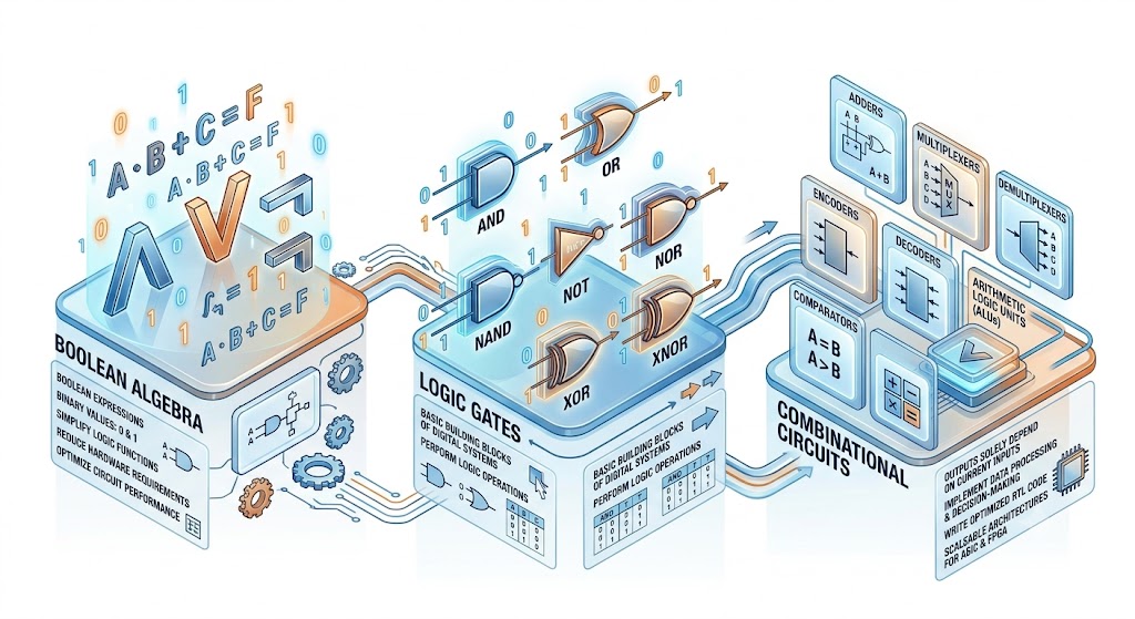
Boolean Algebra, Logic Gates, and Combinational Circuits form the foundation of digital electronics and are essential concepts for every aspiring RTL Design Engineer. Boolean Algebra is a mathematical system used to represent and manipulate binary values, where variables take only two states: 0 and 1. Using Boolean expressions, engineers can simplify complex logic functions, reduce hardware requirements, and optimize circuit performance. Logic gates such as AND, OR, NOT, NAND, NOR, XOR, and XNOR are the basic building blocks of digital systems, performing specific logical operations on binary inputs to produce desired outputs. A strong understanding of these concepts is crucial for designing efficient and reliable digital hardware.
Combinational circuits are digital circuits whose outputs depend solely on the current input values, without relying on previous states or memory elements. Common examples include adders, subtractors, multiplexers, demultiplexers, encoders, decoders, comparators, and arithmetic logic units (ALUs). In RTL design, engineers frequently use combinational logic to implement data processing, decision-making, and control functionalities within larger digital systems. Mastering Boolean Algebra and combinational circuit design helps engineers write optimized RTL code, improve chip performance, reduce power consumption, and create scalable hardware architectures for ASIC and FPGA applications.
Learning Verilog and SystemVerilog: Core Programming Languages for RTL Design and Verification
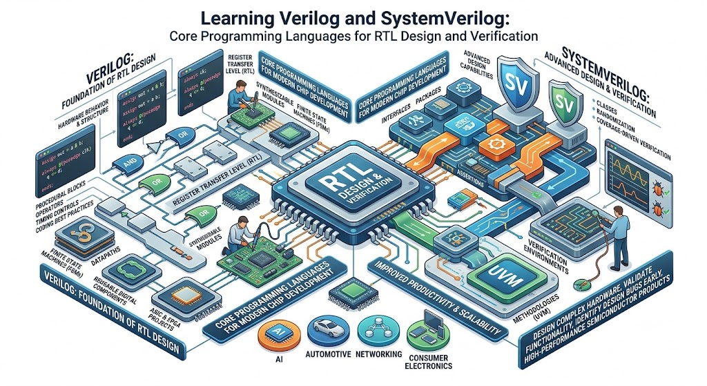
Verilog and SystemVerilog are the most widely used Hardware Description Languages (HDLs) in the semiconductor industry and serve as the foundation of RTL design and verification. Verilog is primarily used to describe digital hardware behavior and structure at the Register Transfer Level (RTL), enabling engineers to model combinational and sequential circuits efficiently. Through Verilog, designers can create synthesizable hardware modules, implement finite state machines (FSMs), design datapaths, and develop reusable digital components for ASIC and FPGA projects. A strong understanding of Verilog syntax, procedural blocks, operators, timing controls, and coding best practices is essential for building reliable and optimized digital designs.
SystemVerilog extends Verilog by introducing advanced design and verification features that improve productivity and scalability in modern chip development. In addition to RTL design capabilities, SystemVerilog provides powerful constructs such as interfaces, packages, assertions, classes, randomization, and coverage-driven verification. These features make it the preferred language for developing sophisticated verification environments and implementing methodologies such as UVM (Universal Verification Methodology). By mastering both Verilog and SystemVerilog, aspiring RTL Design and Verification Engineers gain the ability to design complex hardware, validate functionality effectively, identify design bugs early, and contribute to the development of high-performance semiconductor products used in AI, automotive, networking, and consumer electronics applications.
RTL Coding Guidelines, Design Methodologies, and Best Practices for ASIC and FPGA Development
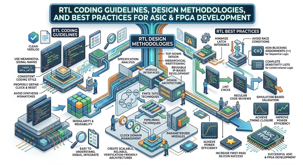
RTL coding guidelines are a set of industry-standard practices that help engineers write clean, synthesizable, and maintainable hardware description code for ASIC and FPGA development. Following proper coding standards ensures that RTL designs are easy to understand, debug, and integrate with larger systems. Engineers should use meaningful signal names, maintain consistent coding styles, properly define clock and reset structures, and avoid constructs that may lead to synthesis mismatches or unintended hardware behavior. Writing modular and reusable RTL code not only improves design quality but also reduces development time and simplifies future enhancements.
Effective RTL design methodologies focus on creating scalable, reliable, and verification-friendly hardware architectures. Engineers typically begin by analyzing design specifications, defining module interfaces, partitioning functionality into smaller blocks, and developing a clear architecture before writing code. Common methodologies include top-down design, bottom-up design, hierarchical design, and reusable IP-based development. Proper implementation of finite state machines (FSMs), pipelining techniques, clock domain management, and parameterized modules helps improve performance, reduce resource utilization, and enhance overall design flexibility. These methodologies are widely adopted in modern ASIC and FPGA projects to manage increasing design complexity.
Following RTL best practices is critical for achieving successful synthesis, verification, and silicon implementation. Designers should minimize latch inference, avoid race conditions, use non-blocking assignments for sequential logic, and ensure complete sensitivity lists for combinational logic. Regular code reviews, linting checks, simulation-based validation, and adherence to timing and power constraints help identify issues early in the development cycle. For both ASIC and FPGA development, high-quality RTL design reduces design iterations, improves timing closure, enhances power efficiency, and increases the likelihood of first-pass silicon success, making it a vital skill for every RTL Design and Verification Engineer.
Functional Verification Fundamentals: Testbenches, Simulation, Debugging, and Coverage Analysis
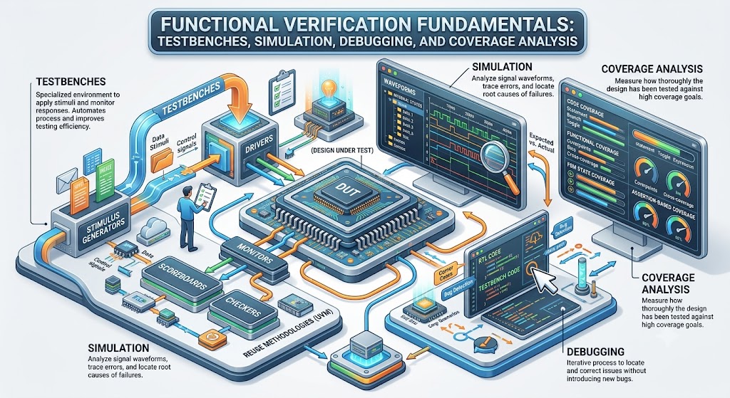
Functional verification is one of the most critical phases of the VLSI design cycle, ensuring that an RTL design behaves exactly as intended before it moves to synthesis and physical implementation. The primary goal of verification is to identify design bugs and functional issues early, reducing costly errors later in the development process. Verification engineers create testbenches—specialized environments that apply input stimuli to the design under test (DUT) and monitor its responses. Using simulation tools, engineers can validate design functionality under various operating conditions, corner cases, and real-world scenarios. A well-structured testbench typically includes stimulus generators, drivers, monitors, scoreboards, and checkers that help automate the verification process and improve testing efficiency.
Simulation, debugging, and coverage analysis work together to ensure comprehensive design validation. During simulation, engineers analyze waveforms, signals, and internal states to detect unexpected behavior and locate the root cause of failures. Debugging involves tracing errors, correcting RTL or testbench issues, and verifying that fixes do not introduce new problems. Coverage analysis measures how thoroughly the design has been tested by tracking metrics such as code coverage, functional coverage, branch coverage, toggle coverage, and state machine coverage. By achieving high coverage goals and thoroughly verifying all design features, engineers can significantly improve design quality, minimize silicon re-spins, and increase confidence that the ASIC or FPGA will function correctly in real-world applications.
Mastering UVM (Universal Verification Methodology) for Advanced Chip Verification
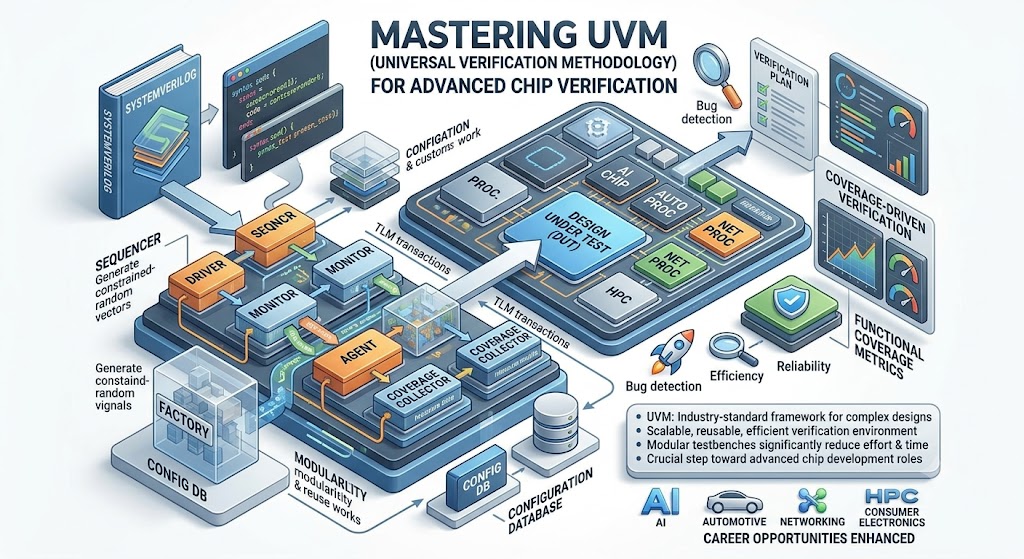
The Universal Verification Methodology (UVM) is the industry-standard framework for building scalable, reusable, and efficient verification environments for complex ASIC and SoC designs. Developed on top of SystemVerilog, UVM provides a structured approach to functional verification by standardizing the way verification components are created and connected. As semiconductor designs become increasingly sophisticated, traditional verification methods often struggle to manage growing complexity. UVM addresses this challenge by enabling engineers to develop modular testbenches that can be reused across multiple projects, significantly reducing verification effort and development time. For aspiring Verification Engineers, mastering UVM is a crucial step toward working on advanced chip development projects in leading semiconductor companies.
A typical UVM verification environment consists of components such as sequencers, drivers, monitors, agents, scoreboards, and coverage collectors. These components work together to generate constrained-random test scenarios, drive stimulus to the Design Under Test (DUT), monitor responses, and automatically compare expected and actual results. UVM also supports powerful features such as transaction-level modeling (TLM), factory patterns, configuration databases, and reporting mechanisms, making it easier to build flexible and scalable verification architectures. Through these capabilities, engineers can efficiently verify complex protocols, processors, memory subsystems, and System-on-Chip (SoC) designs while improving bug detection and verification coverage.
Mastering UVM requires a strong understanding of SystemVerilog, object-oriented programming concepts, verification planning, and coverage-driven verification techniques. Engineers should gain hands-on experience by creating UVM testbenches, implementing reusable verification components, developing constrained-random test cases, and analyzing functional coverage metrics. Since UVM is widely adopted across the semiconductor industry, expertise in this methodology significantly enhances career opportunities in verification engineering. Companies developing AI chips, automotive processors, networking devices, consumer electronics, and high-performance computing systems actively seek professionals with strong UVM skills to ensure the reliability and quality of next-generation semiconductor products.
Industry-Standard EDA Tools Used in RTL Design and Verification Engineering
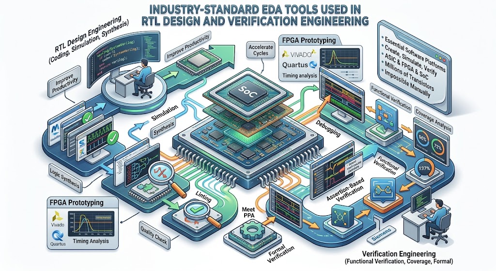
Electronic Design Automation (EDA) tools are essential software platforms used throughout the semiconductor design and verification process. RTL Design and Verification Engineers rely on these tools to create, simulate, analyze, verify, and optimize digital hardware designs before fabrication. As modern ASICs, FPGAs, and System-on-Chip (SoC) devices contain millions or even billions of transistors, manual design and verification are impossible without advanced EDA solutions. These tools help engineers improve productivity, reduce design errors, accelerate development cycles, and ensure that designs meet performance, power, area, and timing requirements.
For RTL design, engineers commonly use tools for coding, simulation, synthesis, linting, and static analysis. Popular simulation tools such as ModelSim, QuestaSim, VCS, and Xcelium enable designers to validate RTL functionality and debug designs through waveform analysis. Synthesis tools like Design Compiler and Genus convert RTL code written in Verilog or SystemVerilog into gate-level netlists suitable for implementation. Linting and quality-check tools help identify coding violations, potential bugs, and synthesis issues early in the design cycle, improving code quality and reducing development risks. FPGA developers also use vendor-specific platforms such as Vivado and Quartus for design implementation, timing analysis, and hardware prototyping.
In verification engineering, advanced EDA tools support functional verification, coverage analysis, formal verification, and debugging activities. Engineers use UVM-compatible simulators, coverage tools, assertion-based verification platforms, and formal verification solutions to validate design correctness under a wide range of operating conditions. Debugging tools provide detailed waveform visualization, signal tracing, and root-cause analysis capabilities that help teams identify and resolve issues efficiently. Familiarity with industry-standard EDA tools is a highly valued skill in the semiconductor industry because it enables engineers to work effectively on complex chip development projects and contribute to faster, higher-quality product delivery.
Conclusion
Becoming a successful RTL Design and Verification Engineer requires a strong combination of theoretical knowledge, practical skills, and continuous learning. From mastering digital electronics fundamentals, Boolean algebra, and combinational logic to learning Verilog, SystemVerilog, RTL coding methodologies, functional verification, and UVM, each step plays a vital role in building a solid foundation for a career in VLSI design. Understanding industry-standard EDA tools and gaining hands-on experience through real-world projects further strengthens your expertise and prepares you for the challenges of modern ASIC and FPGA development. As semiconductor technologies continue to evolve with advancements in AI, automotive electronics, 5G, and high-performance computing, the demand for skilled RTL Design and Verification Engineers is expected to grow significantly.
By following this complete roadmap and consistently developing your technical and problem-solving abilities, you can position yourself for rewarding opportunities in the semiconductor industry. Focus on building strong RTL design skills, developing robust verification techniques, and working on practical projects that showcase your capabilities to employers. Whether your goal is to become an RTL Design Engineer, Verification Engineer, FPGA Developer, or SoC Design Specialist, a structured learning approach and hands-on experience will help you stand out in a competitive job market. With dedication, persistence, and continuous upskilling, you can build a successful and future-proof career in RTL design and verification engineering.