
Future of VLSI in India: Trends and Opportunities
Navigate through this article using the table of contents below
Table of Contents
No headings found in this article.
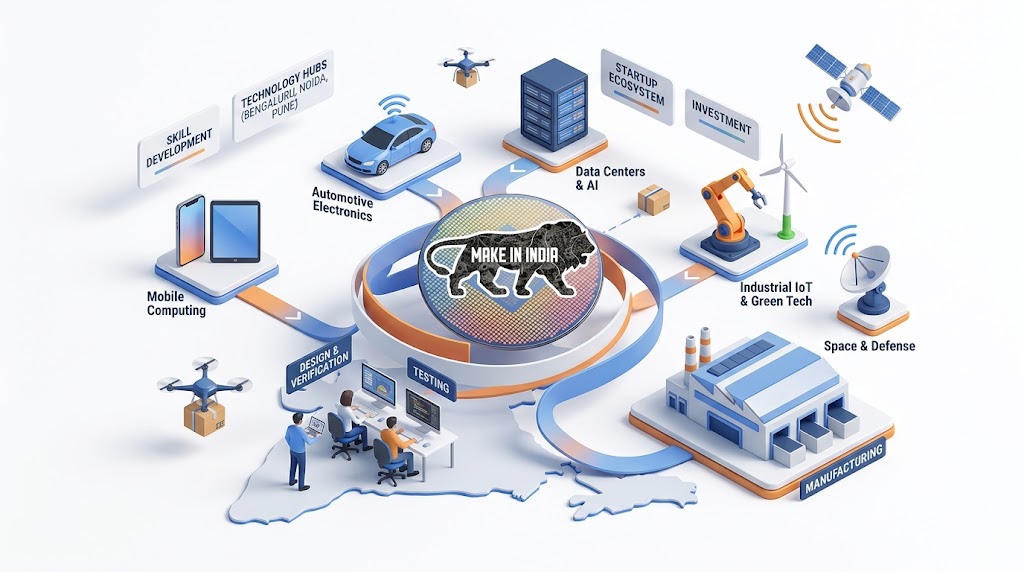
India’s semiconductor story stopped being a “future plan” sometime in early 2026 — fabs are now physically running, not just announced. Most career blogs haven’t caught up to what that actually means for VLSI jobs.
If you’re evaluating whether to build a career in VLSI right now, the honest answer depends on details almost nobody is covering: which fabs are live, which cities are emerging, and which specific skills are getting hired for. Here’s the real picture.
Where India’s Semiconductor Buildout Actually Stands in 2026
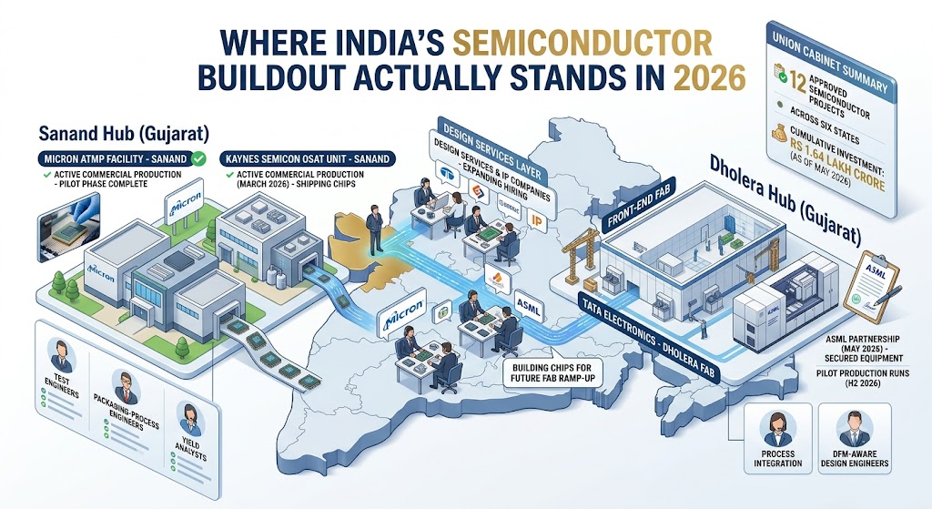
Unlike the vague “fabs are coming” language in most VLSI career posts, the situation has concrete, dated milestones. Micron’s Assembly, Test, Marking, and Packaging (ATMP) facility in Sanand, Gujarat moved from pilot phase into active commercial production, becoming the first fully operational facility of the current mission cycle. Kaynes Semicon’s OSAT unit, also in Sanand, reached commercial production in March 2026 — just fourteen months after breaking ground — and has already begun shipping chips.
On the front-end side, Tata Electronics signed a strategic partnership with ASML in May 2026 to secure lithography equipment for its Dholera fab, positioning that facility for pilot production runs in the second half of 2026. As of May 2026, the Union Cabinet had approved a total of 12 semiconductor projects across six states, with cumulative investment around Rs 1.64 lakh crore.
This matters for job-seekers because it changes the type of roles opening up:
• ATMP and OSAT facilities (already running) need test engineers, packaging-process engineers, and yield analysts — roles barely covered in design-focused career content
• Dholera’s fab, once in pilot production, will need process integration and DFM-aware design engineers who understand foundry constraints, not just RTL theory
• Design services and IP companies are expanding hiring now, ahead of fab ramp-up, to build the chip designs that will eventually run through these facilities
The Geography of Opportunity Is Shifting Beyond Bangalore
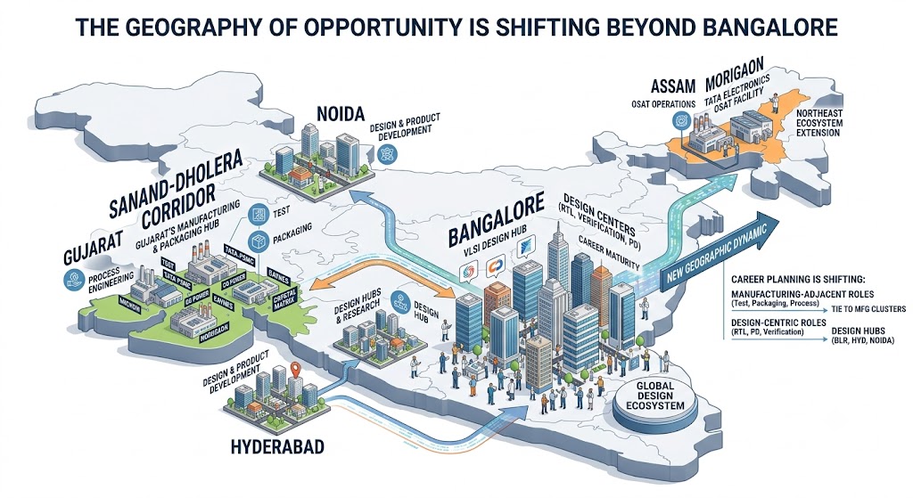
Bangalore still accounts for the majority of VLSI design activity in India, but the job map is actively expanding. Gujarat’s Sanand-Dholera corridor has become the country’s manufacturing and packaging hub, hosting Micron, Tata-PSMC, CG Power, Kaynes, and Crystal Matrix within a tight geographic radius. Assam has entered the picture too, with Tata Electronics’ OSAT facility in Morigaon extending the ecosystem into the Northeast.
For engineers, this geographic spread is a genuinely new dynamic: roles in test, packaging, and process engineering are increasingly tied to these manufacturing clusters, while pure design-engineering roles (RTL, verification, physical design) remain concentrated in Bangalore, Hyderabad, and Noida design centers. Career planning now has to account for this split — the manufacturing-adjacent roles and the design-centric roles are no longer in the same cities by default.
AI Is Changing How Chips Get Designed — Not Just What They Power
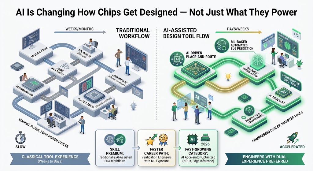
Most career content mentions AI only as a demand driver (“chips for AI hardware”). The more important shift for working engineers is that AI is changing the design process itself. AI-driven place-and-route tools and machine-learning-based verification are compressing design cycles that used to take weeks into days, and companies are actively hiring engineers who can work alongside these tools rather than only through traditional manual flows.
This creates a specific, often-overlooked skill premium:
• Engineers who understand both traditional EDA workflows and AI-assisted design tools are increasingly preferred over those with only classical tool experience
• Verification engineers with exposure to ML-based coverage and bug-prediction tools are seeing faster movement into senior roles
• Chip designs optimized specifically for AI accelerators (NPUs, edge inference chips) represent one of the fastest-growing design categories in 2026
Chiplets and Compound Semiconductors: The Quiet New Opportunity Track
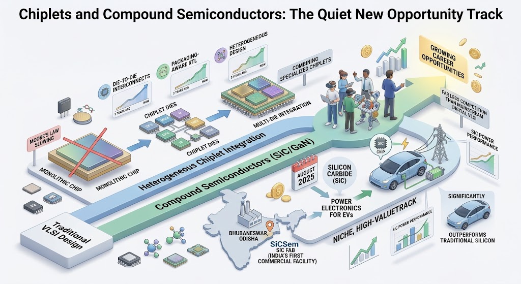
As Moore’s Law scaling slows, the industry has shifted toward chiplet-based design — combining multiple smaller dies into a single package instead of pushing monolithic chips to ever-smaller nodes. This is opening design roles focused on die-to-die interconnects, packaging-aware RTL, and heterogeneous integration, none of which were significant career categories even three years ago.
India is also building real capacity in compound semiconductors. SiCSem’s Silicon Carbide fab in Bhubaneswar, Odisha — India’s first commercial SiC compound semiconductor facility — was approved in August 2025, opening a niche but high-value track for engineers interested in power electronics for EVs, where SiC chips significantly outperform traditional silicon. Engineers who position early in chiplet integration or compound semiconductor design are entering a track with far less competition than mainstream digital VLSI.
How to Actually Position Yourself for This Wave — Not Just Watch It Happen
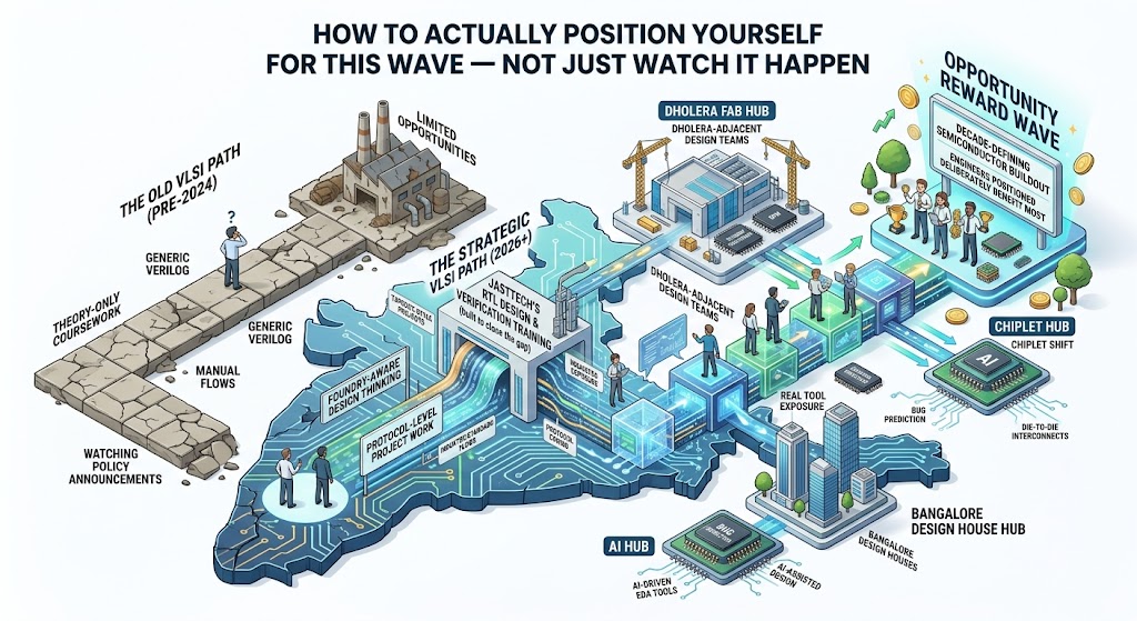
Given where the fabs, the geography, and the skill demands are actually heading, the practical path for someone entering VLSI now looks different than it did even two years ago. It means choosing training that reflects current industry conditions — foundry-aware design thinking, real tool exposure, and protocol-level project work — rather than theory-only coursework.
This is the specific gap JastTech’s RTL Design and Verification training is built to close. Rather than teaching Verilog in isolation, the program structures learning around tapeout-style projects and industry-standard tool flows, giving learners direct exposure to the kind of foundry-aware, protocol-level work that Dholera-adjacent design teams and Bangalore design houses are actively hiring for in 2026.
India’s semiconductor buildout has moved from policy announcement to physical infrastructure, and the opportunity window for engineers is real — but it rewards specific, current, industry-tested skills far more than generic VLSI familiarity. The engineers who position deliberately around where the fabs, the AI-driven tools, and the chiplet shift are actually heading will be the ones who benefit most from this decade-defining buildout.
Conclusion
India’s semiconductor industry has entered a new phase where manufacturing facilities are operational, major fabs are progressing toward production, and the demand for skilled VLSI professionals is expanding across both design and manufacturing domains. With emerging semiconductor hubs in Gujarat, Odisha, Assam, Bangalore, Hyderabad, and Noida, engineers now have access to a wider range of career paths than ever before. At the same time, advancements in AI-assisted chip design, chiplet architectures, and compound semiconductors are reshaping the skills employers expect from the next generation of semiconductor professionals.
For aspiring VLSI engineers, this is an ideal time to build expertise in industry-relevant areas such as RTL design, functional verification, physical design, DFT, packaging, and process-aware design methodologies. Practical training, hands-on projects, and proficiency with modern EDA tools will be the key differentiators in a competitive job market. As India's semiconductor ecosystem continues to grow from design services to full-scale manufacturing, professionals who invest in current technologies and real-world experience will be well positioned to secure rewarding careers and contribute to the country's rapidly expanding chip industry.