
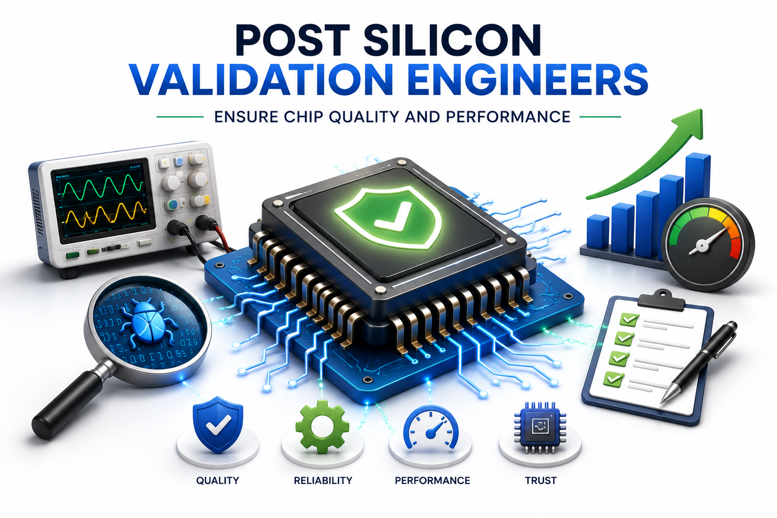
How Post Silicon Validation Engineers Ensure Chip Quality and Performance
Navigate through this article using the table of contents below
Table of Contents
No headings found in this article.
Every chip you depend on — the processor in your laptop, the modem in your phone, the AI accelerator in a data center — passed through a brutal final exam before reaching you. That exam is called post-silicon validation, and it is the last line of defense between a billion-dollar chip tape-out and a catastrophic field failure. Only 14% of ASIC and SoC projects achieve first-silicon success without major issues, according to the 2024 Wilson Research Group / Siemens EDA Functional Verification Study — the lowest figure in more than twenty years of tracking. That single statistic tells you everything about why post-silicon validation engineers are among the most critical — and most in-demand — professionals in the semiconductor industry.
Post-silicon validation is not simply 'testing a chip.' It is a rigorous, multi-phase engineering discipline that combines hardware lab skills, firmware development, signal analysis, and increasingly, AI-driven automation. In this blog, we break down exactly what post-silicon validation engineers do, what tools they use, what bugs they catch, and why this is one of the most rewarding and lucrative careers in India's booming semiconductor ecosystem in 2025.
What Is Post-Silicon Validation? Pre-Silicon vs. Real-World Testing

Post-silicon validation refers to the comprehensive testing and validation of a semiconductor chip on actual fabricated silicon — not a virtual model or simulation. When the first physical chips return from the foundry (called first silicon or ES1 — Engineering Sample 1), a team of post-silicon validation engineers takes over. Their job is to confirm that the physical chip behaves exactly as the RTL design specified, at real operating speeds, under real electrical conditions.
This is fundamentally different from pre-silicon verification, which uses SystemVerilog testbenches, UVM environments, and formal tools to check a software model of the chip. Pre-silicon verification is fast and iterative but cannot replicate physical reality: signal integrity, electromagnetic interference, PVT (process-voltage-temperature) corners, and inter-module timing skews only reveal themselves when electrons flow through actual transistors. That is the gap post-silicon validation closes.
Key distinctions between the two phases:
• Pre-silicon: virtual RTL/gate simulations, UVM testbenches, emulation platforms — no real hardware
• Post-silicon: real chip on a validation board, running at full speed with lab instruments attached
• Pre-silicon can miss: signal integrity issues, IR drop effects, cross-chip coupling, and subtle CDC failures
• Post-silicon confirms: actual timing margins, power consumption, thermal behavior, and interface protocol compliance
• A mask re-spin at an advanced node (5nm, 7nm) can cost over $1 million — PSV exists to prevent this
2. Silicon Bring-Up: The First Critical Phase of Post-Silicon Validation
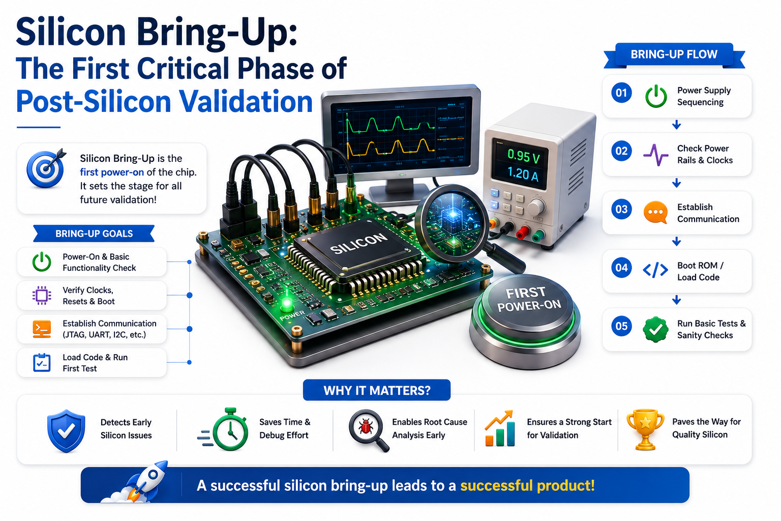
The most nerve-wracking moment in any chip program is silicon bring-up — the process of powering up a brand-new chip for the very first time. Nothing is guaranteed. The chip that spent 18 months in design and layout and hundreds of millions of dollars to manufacture might not even boot. The post-silicon validation engineer's first job is to methodically bring the chip to life, one subsystem at a time.
The bring-up process follows a strict sequence. Engineers begin with power sequencing — carefully applying supply voltages (VDD, VDDQ, VDDIO) in the correct order while monitoring current draw. An unexpected spike can indicate a short circuit; too little current may mean clocks are not running. Once power is stable, engineers verify that the chip's internal clocks are toggling at the correct frequencies using an oscilloscope. They then establish communication via JTAG (IEEE 1149.1), the universal debug interface that allows register reads/writes without the chip fully booting.
The structured silicon bring-up checklist includes:
• Power sequencing: verify all supply rails within tolerance; monitor for latch-up or short-circuit events
• Clock and reset: confirm PLLs lock at target frequency; verify reset deasserts cleanly
• JTAG connectivity: read chip ID register as the first sanity check — if this fails, nothing else matters
• Firmware boot: load a minimal bootloader via JTAG and confirm the primary CPU executes instructions
• Memory subsystem: validate DDR/LPDDR training sequence completes and passes read/write stress tests
• Peripheral block validation: systematically verify UART, PCIe, USB, Ethernet, and other IP blocks
3. Lab Instruments and Tools Every Post-Silicon Validation Engineer Uses

Post-silicon validation is fundamentally a lab discipline, and the tools it uses are as specialized as the chips being tested. Unlike software testing or even pre-silicon verification, post-silicon validation requires hands-on proficiency with both hardware measurement instruments and software automation frameworks. The modern PSV lab looks nothing like it did even five years ago — AI and cloud platforms have transformed what was once a manual, single-bench process into a distributed, automated validation ecosystem.
On the hardware side, the oscilloscope is the post-silicon validation engineer's most essential tool — used for capturing waveforms, measuring timing margins, and diagnosing signal integrity issues. Logic analyzers decode complex multi-wire digital buses in real time. Protocol analyzers (for PCIe, USB 4.0, MIPI, DDR5) capture and decode high-speed serial traffic. JTAG debuggers enable direct on-chip register access even when no operating system is running. And Automated Test Equipment (ATE) systems like Teradyne or Advantest platforms execute high-volume production test patterns.
Modern post-silicon validation tools and frameworks (2025):
• Oscilloscopes (Keysight / Tektronix): waveform capture at 20+ GHz bandwidth for high-speed signals
• Protocol analyzers: PCIe Gen 5, USB4, DDR5, CXL — protocol-layer debug for multi-interface SoCs
• JTAG/cJTAG debuggers: OpenOCD, ARM DS-5, proprietary SoC debug tools for register-level access
• Advantest SiConic: unified platform automating data collection from bring-up through final sign-off
• IEEE 1687 (IJTAG): standardized on-chip instrument access — reusable across chip generations
• Python and Tcl automation: scripted regression suites that reduce manual test execution by 80%+
• Cloud validation platforms: parallel execution across geographies with centralized waveform/log viewers
4. What Bugs Does Post-Silicon Validation Actually Catch?

The highest-stakes question in any chip program is simple: what did simulation miss? Post-silicon validation exists precisely because pre-silicon verification — even with 100% code coverage, UVM constrained-random tests, and formal property checking — cannot fully replicate physical silicon behavior. The class of bugs that escape pre-silicon and surface in the lab are often the most expensive and embarrassing: Intel's famous Pentium FDIV bug (a $475 million recall), or NVIDIA's Blackwell GPU server overheating issues that required rack redesign before mass deployment.
Post-silicon validation engineers are trained to find several distinct bug categories. Timing violations are the most common — where a signal arrives at a flip-flop too late (setup violation) or too early (hold violation) under actual PVT conditions that simulation could not precisely model. Signal integrity problems manifest as bit errors on high-speed serial links (PCIe, DDR) due to crosstalk, impedance mismatches, or jitter accumulation. Power-related bugs — such as excessive IR drop causing logic failures at low voltage corners — only appear when real current flows through real metal wires.
Categories of bugs uniquely caught by post-silicon validation:
• Timing violations: setup/hold failures at speed corners not fully captured in static timing analysis
• Signal integrity: eye diagram failures on PCIe/USB/DDR lanes from crosstalk and reflection
• Power/thermal: IR drop causing functional errors; hot spots triggering thermal shutdown
• Clock domain crossing failures: metastability events that appear statistically in real silicon
• Reset sequencing bugs: incorrect power-up behavior under fast ramp rates
• Functional corner cases: behaviors triggered only by specific workloads that no testbench modeled
• Manufacturing variation effects: process corner outliers that fall outside nominal simulation parameters
5. Post-Silicon Validation Engineer: Skills, Career Path, and Salaries in India

The post-silicon validation engineer role sits at the intersection of hardware, software, and systems — making it one of the broadest, most technically demanding positions in the semiconductor industry. A strong PSV engineer needs to understand chip architecture deeply enough to know what to test, be comfortable in a lab environment with expensive instruments, and write Python or C code well enough to automate complex test sequences. It is not a role for specialists — it demands generalist excellence.
In India, this role is among the fastest-growing in the semiconductor hiring wave of 2025. Glassdoor data (November 2025) shows an average post-silicon validation engineer salary in India of ₹8.70 LPA, with top earners reaching ₹26.40 LPA. Leading companies hiring aggressively for this role in India include Intel (Bengaluru, Hyderabad), AMD (Bengaluru), Qualcomm, Texas Instruments (Bengaluru), NVIDIA, ARM, and Marvell. With India's semiconductor design GCC count projected to grow 30% by 2030, demand for PSV engineers will only intensify.
Essential skills for a post-silicon validation engineer role:
• SoC architecture knowledge: ability to read chip specifications, micro-architecture documents, and block diagrams
• Digital electronics fundamentals: timing analysis, clock domains, signal integrity, power distribution
• Lab instrument proficiency: oscilloscopes, logic analyzers, protocol analyzers, JTAG debuggers
• Firmware and embedded C: ability to write bring-up code, register access routines, and test drivers
• Python / Tcl scripting: test automation, data parsing, regression frameworks
• Debug mindset: systematic root-cause analysis — knowing when a failure is a design bug vs. a test setup issue
• Interfaces knowledge: PCIe, DDR, USB, MIPI, Ethernet — protocol-level understanding for debug
6. The Future of Post-Silicon Validation: AI, Cloud, and the 2025–2030 Outlook

Post-silicon validation is undergoing its most significant transformation in decades. Three forces are reshaping the discipline simultaneously: AI-driven automation, cloud-based distributed lab infrastructure, and the explosive complexity of chiplet-based SoC designs. Engineers who understand only traditional bench validation will find themselves outpaced — but those who embrace these shifts will command the most valuable positions in the next generation of chip programs.
Artificial intelligence is being applied to the most time-consuming part of PSV: log analysis and bug classification. Modern chips running complex workloads generate terabytes of trace data per validation run. Machine learning models — both supervised (classifying known failure signatures) and unsupervised (surfacing anomalous patterns) — are dramatically reducing the time engineers spend on manual log review. By 2025, cloud validation platforms have already reduced validation timelines for edge AI chips by enabling parallel execution across global teams. The shift-left approach — using emulation-silicon hybrid environments to pre-validate test sequences before silicon arrives — is further compressing bring-up cycles.
Key trends shaping post-silicon validation through 2030:
• AI log analysis: ML classifiers that flag silicon failures within minutes of test completion, not hours
• Cloud validation: remote labs enabling Indian PSV teams to run tests on silicon housed in US or Taiwan facilities
• IEEE 1687 (IJTAG) standardization: reusable on-chip instrument networks reducing per-chip bring-up time
• Chiplet validation: new multi-die bring-up sequences needed as UCIe-based chiplet SoCs proliferate
• Autonomous debug agents: LLM-based tools that correlate failing assertions with RTL root causes automatically
• Zero-respin target: predictive AI models that flag layout/physical design choices most likely to cause PSV failures