
How RTL Design and Verification Reduce Chip Development Risks
Navigate through this article using the table of contents below
Table of Contents
No headings found in this article.
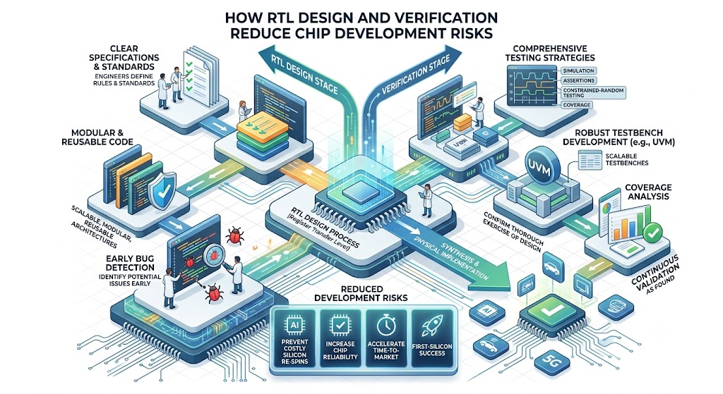
What if a single undetected design bug could cost millions of dollars and delay a semiconductor product launch by months? In today's highly competitive semiconductor industry, developing complex System-on-Chip (SoC) and ASIC solutions requires extreme precision at every stage of the design cycle. This is where RTL design and verification play a critical role. By identifying functional errors, design flaws, and performance bottlenecks early in the development process, RTL design and verification significantly reduce the risks associated with chip development, helping companies avoid costly silicon re-spins and project delays.
RTL (Register Transfer Level) design serves as the foundation of digital chip development, while verification ensures that the design behaves exactly as intended before fabrication. Together, these processes improve design quality, enhance reliability, and accelerate time-to-market. As modern chips become increasingly complex for applications such as artificial intelligence, automotive electronics, 5G communication, and consumer devices, robust RTL design and comprehensive verification methodologies have become essential for minimizing development risks and ensuring first-silicon success. For students and early-career engineers looking to build expertise in these areas, RTL design and verification training can provide practical exposure to industry-standard tools, coding practices, and verification techniques. Understanding how RTL design and verification work together can help engineers and organizations build high-performance, error-free semiconductor products more efficiently.
Importance of RTL Design in Modern Semiconductor Chip Development
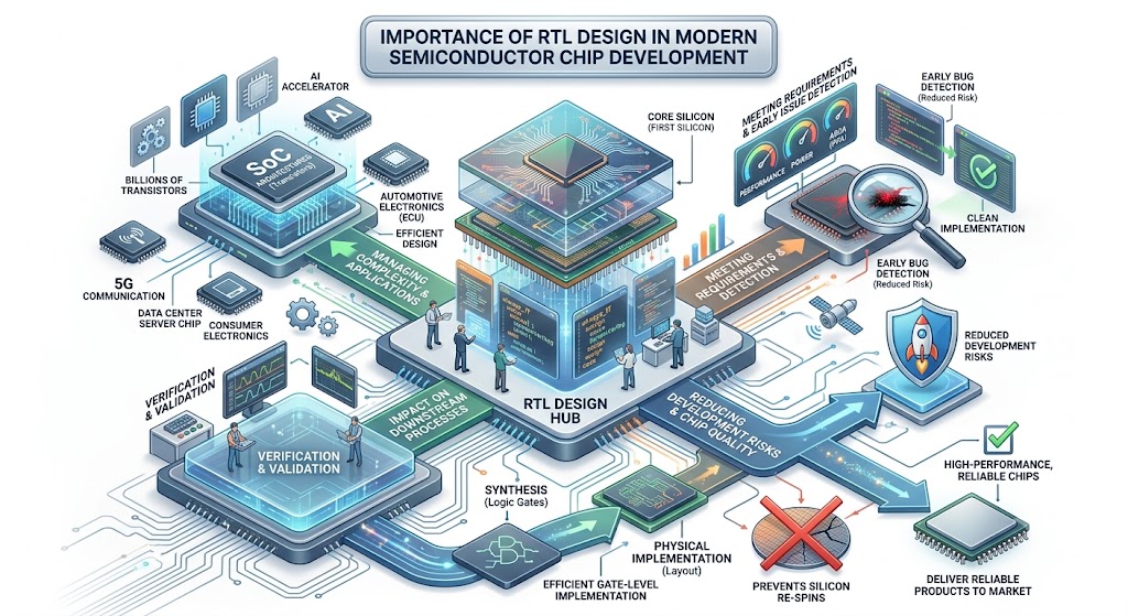
RTL (Register Transfer Level) design is one of the most critical stages in modern semiconductor chip development, serving as the bridge between system-level specifications and physical hardware implementation. At this stage, engineers describe how digital circuits process, store, and transfer data using hardware description languages such as Verilog and SystemVerilog. RTL design defines the functional behavior of a chip before it is synthesized into logic gates, making it the foundation upon which the entire semiconductor development process is built. A well-structured RTL design ensures that the chip meets performance, power, and area requirements while minimizing the risk of design errors.
As semiconductor devices become increasingly complex, RTL design plays a vital role in managing millions or even billions of transistors within modern System-on-Chip (SoC) architectures. Applications such as artificial intelligence, automotive electronics, 5G communication systems, data centers, and consumer electronics demand highly efficient and reliable chip designs. RTL designers must create scalable, modular, and reusable architectures that support advanced functionality while maintaining design efficiency. By establishing a clear and accurate representation of the intended hardware behavior, RTL design helps development teams identify potential issues early in the design cycle, reducing costly modifications later in the project.
Another major importance of RTL design lies in its impact on verification, synthesis, and overall chip quality. A clean and optimized RTL implementation enables verification engineers to perform comprehensive testing and validation before manufacturing. It also allows synthesis tools to generate efficient gate-level implementations that meet timing and power targets. Since errors discovered after fabrication can result in expensive silicon re-spins and delayed product launches, investing time in robust RTL design significantly reduces development risks. Ultimately, RTL design serves as the cornerstone of successful semiconductor chip development, enabling organizations to deliver high-performance, reliable, and cost-effective products to market.
Know More About :- RTL Design and Verification Training in Hyderabad
Common Chip Design Risks and Challenges Faced by Semiconductor Companies
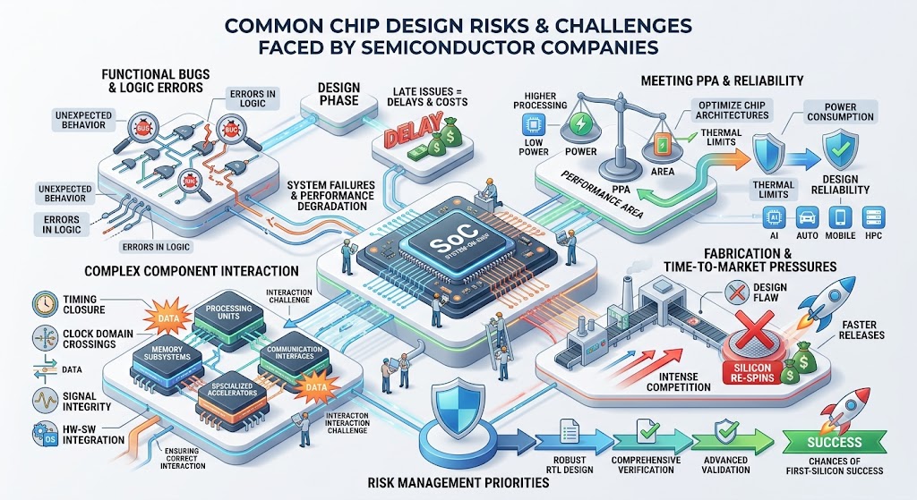
Modern semiconductor companies face numerous chip design risks and challenges as integrated circuits become increasingly complex and feature-rich. One of the most significant risks is the introduction of functional bugs during the design phase. Even a small error in logic implementation can cause unexpected behavior, system failures, or performance degradation in the final product. As System-on-Chip (SoC) designs integrate multiple processing units, memory subsystems, communication interfaces, and specialized accelerators, ensuring correct interaction between all components becomes a major engineering challenge. Detecting and fixing these issues late in the development cycle can lead to substantial project delays and increased development costs.
Another major challenge is meeting stringent power, performance, and area (PPA) requirements while maintaining design reliability. Semiconductor companies must optimize chip architectures to deliver higher processing capabilities without exceeding power consumption and thermal limits. This becomes particularly critical in applications such as artificial intelligence, automotive electronics, mobile devices, and high-performance computing systems. Designers must also address timing closure issues, clock domain crossings, signal integrity concerns, and hardware-software integration complexities. Failure to properly manage these factors can result in chips that do not meet market expectations or fail to operate under real-world conditions.
Manufacturing and time-to-market pressures further increase the risks associated with chip development. A design flaw discovered after fabrication can lead to costly silicon re-spins, requiring additional design iterations and significantly increasing project expenses. At the same time, intense competition in the semiconductor industry demands faster product releases, leaving less room for design mistakes. Verification challenges, incomplete test coverage, evolving industry standards, and growing design complexity make risk management a critical priority for semiconductor organizations. By implementing robust RTL design practices, comprehensive verification strategies, and advanced validation methodologies, companies can minimize these risks and improve the likelihood of achieving first-silicon success.
How RTL Coding Standards Improve Design Quality and Reduce Errors
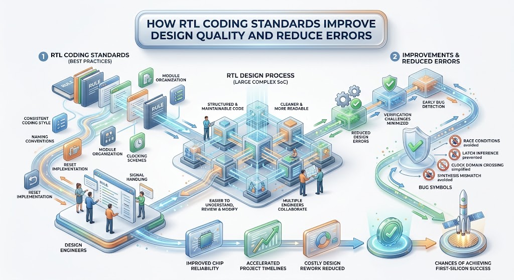
RTL coding standards play a crucial role in improving design quality by ensuring that hardware descriptions are written in a consistent, structured, and maintainable manner. These standards define best practices for coding style, naming conventions, module organization, clocking schemes, reset implementation, and signal handling in hardware description languages such as Verilog and SystemVerilog. By following established RTL coding guidelines, design teams can create cleaner and more readable code that is easier to understand, review, and modify. This consistency becomes especially important in large semiconductor projects where multiple engineers collaborate on complex System-on-Chip (SoC) designs. Many students are first introduced to these industry best practices through a reputable VLSI training institute in India, where practical coding discipline is emphasized alongside theoretical concepts.
Adhering to RTL coding standards also helps reduce design errors and verification challenges throughout the chip development process. Standardized coding practices minimize the risk of introducing bugs related to race conditions, latch inference, clock domain crossing issues, and synthesis mismatches. Well-written RTL code is easier to verify, debug, and optimize, enabling engineers to detect potential problems early before they propagate into later development stages. As a result, semiconductor companies can reduce costly design rework, improve overall chip reliability, accelerate project timelines, and increase the chances of achieving first-silicon success.
Role of Functional Verification in Detecting Design Bugs Early
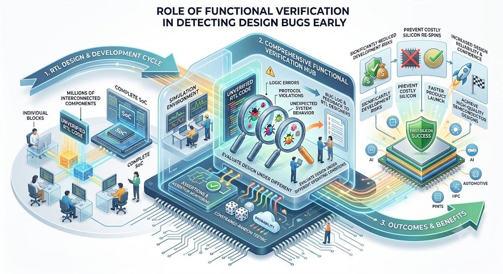
Functional verification is a critical phase in semiconductor chip development that ensures an RTL design behaves according to its intended specifications before fabrication. Its primary objective is to identify design bugs, logic errors, protocol violations, and unexpected system behaviors at the earliest possible stage of the development cycle. Verification engineers use simulation environments, testbenches, assertions, and constrained-random testing techniques to evaluate how the design responds under different operating conditions. Since modern System-on-Chip (SoC) designs contain millions of interconnected components, functional verification helps confirm that each block and subsystem operates correctly both individually and as part of the complete chip architecture.
Detecting bugs during functional verification significantly reduces development risks and prevents costly issues from reaching silicon. Errors found after fabrication can lead to expensive silicon re-spins, extended project schedules, and delayed product launches. By uncovering problems early, verification teams can work closely with RTL designers to resolve defects before synthesis and manufacturing begin. Comprehensive functional verification also improves design reliability, increases confidence in the final product, and contributes to achieving first-silicon success. As chip complexity continues to grow in applications such as AI, automotive electronics, and high-performance computing, functional verification remains one of the most effective strategies for ensuring high-quality semiconductor designs.
Benefits of Simulation and Debugging During RTL Design and Verification
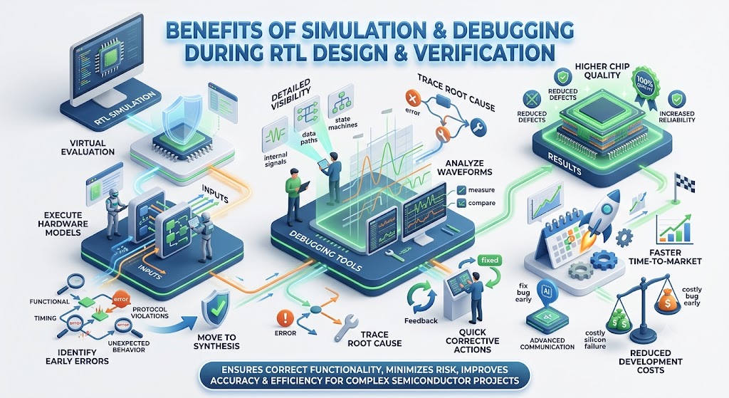
Simulation and debugging are essential components of the RTL design and verification process, enabling engineers to evaluate the functionality of a chip before it is manufactured. RTL simulation allows designers to execute hardware models in a virtual environment and observe how the design responds to various input conditions. By comparing simulation results against design specifications, engineers can identify functional errors, timing issues, protocol violations, and unexpected behaviors early in the development cycle. This proactive approach helps ensure that the design operates correctly before moving to synthesis and fabrication stages.
One of the key benefits of simulation is its ability to reduce development risks and costs by detecting bugs when they are easier and less expensive to fix. Through extensive testing, verification teams can validate different operational scenarios, corner cases, and system interactions without requiring physical hardware. Debugging tools further enhance this process by providing detailed visibility into internal signals, data paths, state machines, and module interactions. Engineers can trace the root cause of failures, analyze waveform data, and quickly implement corrective actions, significantly improving design accuracy and verification efficiency.
Simulation and debugging also contribute to higher chip quality and faster time-to-market. By continuously validating RTL code throughout the development process, teams can prevent defects from propagating into later stages where corrections become more complex and costly. Effective debugging accelerates problem resolution, improves collaboration between design and verification teams, and increases confidence in the overall functionality of the chip. As semiconductor devices become more sophisticated in areas such as artificial intelligence, automotive systems, and advanced communication technologies, simulation and debugging remain indispensable tools for delivering reliable, high-performance semiconductor products while minimizing the risk of silicon failures.
How Coverage Analysis Ensures Complete Verification of Complex SoCs

Coverage analysis is a fundamental aspect of functional verification that helps ensure a complex System-on-Chip (SoC) design has been thoroughly tested before fabrication. As modern SoCs integrate multiple processors, memory blocks, communication interfaces, and specialized hardware accelerators, verifying every possible functional scenario becomes increasingly challenging. Coverage analysis provides measurable data on how much of the design has been exercised during simulation by tracking metrics such as code coverage, functional coverage, branch coverage, toggle coverage, and assertion coverage. These insights help verification teams identify untested areas of the design and determine whether additional test cases are required to achieve comprehensive verification.
By systematically measuring verification progress, coverage analysis reduces the risk of hidden bugs escaping into silicon. It enables engineers to validate that critical features, operating modes, corner cases, and subsystem interactions have been thoroughly exercised under various conditions. Rather than relying solely on the number of test cases executed, coverage-driven verification focuses on the quality and completeness of testing. This approach improves confidence in the RTL design, enhances overall chip reliability, and minimizes the likelihood of costly silicon re-spins. For complex semiconductor projects, coverage analysis serves as a key indicator that verification goals have been met and that the design is ready for successful tape-out and manufacturing.
Reducing Costly Silicon Re-Spins Through Effective RTL Verification Strategies
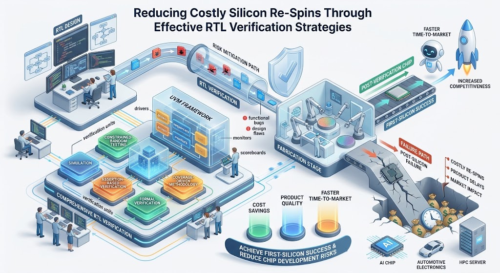
Silicon re-spins are among the most expensive and time-consuming challenges in semiconductor chip development. A silicon re-spin occurs when a fabricated chip contains design errors or functional defects that require modifications and a new manufacturing cycle. These issues can significantly increase development costs, delay product launches, and impact a company's competitiveness in the market. Effective RTL verification strategies help minimize this risk by identifying and correcting design flaws long before the chip reaches the fabrication stage. By thoroughly validating RTL code against design specifications, engineering teams can detect functional bugs early and prevent costly mistakes from being embedded into silicon.
A comprehensive RTL verification approach combines multiple techniques, including simulation, constrained-random testing, assertion-based verification, formal verification, and coverage-driven methodologies. These techniques enable verification engineers to test a wide range of operating conditions, corner cases, and subsystem interactions that may not be apparent during basic functional testing. Advanced verification frameworks such as Universal Verification Methodology (UVM) further improve testbench reusability and scalability, allowing teams to achieve greater verification depth and consistency across complex System-on-Chip (SoC) designs. This systematic verification process helps uncover hidden defects that could otherwise lead to silicon failures after manufacturing.
Reducing silicon re-spins through effective RTL verification delivers substantial benefits in terms of cost savings, product quality, and faster time-to-market. Early bug detection allows design teams to resolve issues when modifications are relatively simple and inexpensive, avoiding the need for redesign and re-fabrication. It also increases confidence that the chip will function correctly under real-world conditions and meet performance, power, and reliability targets. As semiconductor designs continue to grow in complexity for applications such as artificial intelligence, automotive electronics, and high-performance computing, robust RTL verification strategies remain essential for achieving first-silicon success and reducing overall chip development risks.
Importance of Assertion-Based Verification (ABV) in Risk Mitigation
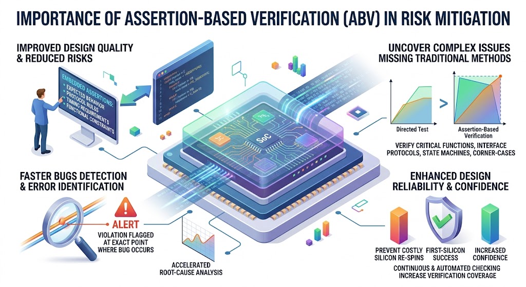
Assertion-Based Verification (ABV) is a powerful verification technique used to improve design quality and reduce risks during semiconductor chip development. Assertions are formal statements embedded within the RTL design or verification environment that define expected design behavior, protocol rules, timing requirements, and functional constraints. During simulation or formal verification, these assertions continuously monitor the design and automatically flag violations whenever the implemented behavior deviates from the specified requirements. This enables verification engineers to detect bugs at the exact point where they occur, making error identification and root-cause analysis significantly faster and more efficient.
The importance of ABV in risk mitigation lies in its ability to uncover complex design issues that traditional testing methods may miss. Assertions help verify critical functions, interface protocols, state machine behavior, and corner-case scenarios throughout the verification process. By providing continuous and automated checking, ABV increases verification coverage, improves bug detection accuracy, and reduces the likelihood of defects escaping into silicon. As modern System-on-Chip (SoC) designs become more sophisticated, Assertion-Based Verification plays a crucial role in preventing costly silicon re-spins, enhancing design reliability, and increasing confidence in achieving first-silicon success.
Universal Verification Methodologies (UVM) for Reliable Chip Development
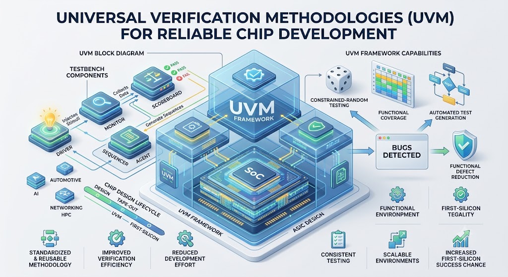
The Universal Verification Methodology (UVM) has become the industry-standard framework for verifying complex semiconductor designs and ensuring reliable chip development. Built on SystemVerilog, UVM provides a standardized and reusable approach for creating scalable verification environments that can handle increasingly sophisticated System-on-Chip (SoC) and ASIC designs. It introduces modular components such as drivers, monitors, scoreboards, sequencers, and agents, allowing verification teams to build structured testbenches that can be reused across multiple projects. This standardized methodology improves verification efficiency, reduces development effort, and enables consistent testing throughout the chip design lifecycle.
One of the key advantages of UVM is its ability to support advanced verification techniques such as constrained-random testing, functional coverage, and automated test generation. These capabilities help engineers explore a wider range of design scenarios, corner cases, and subsystem interactions that might be difficult to test using traditional directed approaches. By improving verification coverage and accelerating bug detection, UVM significantly reduces the risk of functional defects reaching silicon. As semiconductor designs continue to grow in complexity for applications such as artificial intelligence, automotive electronics, networking, and high-performance computing, UVM plays a critical role in enhancing design reliability, reducing development risks, and increasing the likelihood of achieving first-silicon success.
Best Practices for Achieving First-Silicon Success with RTL Design and Verification
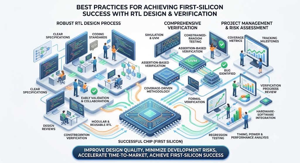
Achieving first-silicon success is one of the primary goals of every semiconductor development project, as it ensures that a chip functions correctly after fabrication without requiring costly redesigns or silicon re-spins. One of the most important best practices is establishing a robust RTL design process based on clear specifications, coding standards, and design reviews. Engineers should create modular, reusable, and well-documented RTL code that is easier to verify and maintain throughout the development lifecycle. Early design validation and continuous collaboration between design and verification teams also help identify potential issues before they become critical problems.
Comprehensive verification is another essential factor in achieving first-silicon success. Verification teams should implement a combination of simulation, constrained-random testing, assertion-based verification, formal verification, and coverage-driven methodologies to thoroughly validate the design. Advanced verification frameworks such as UVM enable scalable and reusable testbench development, allowing engineers to test a wide range of operating conditions, corner cases, and subsystem interactions. Monitoring coverage metrics throughout the verification process helps ensure that all critical functionality has been exercised and that hidden bugs are identified before tape-out.
In addition to strong design and verification practices, effective project management and risk assessment play a crucial role in successful chip development. Teams should continuously track design milestones, review verification progress, and address issues as soon as they are discovered. Performing thorough regression testing, validating hardware-software integration, and analyzing timing, power, and performance requirements further reduce the likelihood of post-silicon failures. By following these best practices, semiconductor companies can improve design quality, minimize development risks, accelerate time-to-market, and significantly increase the chances of achieving first-silicon success in complex SoC and ASIC projects.
Conclusion
As semiconductor devices continue to grow in complexity, the importance of RTL design and verification in reducing chip development risks cannot be overstated. From creating high-quality RTL code and following coding standards to implementing comprehensive functional verification, simulation, debugging, coverage analysis, Assertion-Based Verification (ABV), and UVM-based methodologies, every step plays a critical role in ensuring design correctness and reliability. These practices help engineering teams detect and resolve issues early in the development cycle, significantly reducing the chances of costly silicon re-spins, project delays, and product failures.
Ultimately, effective RTL design and verification form the foundation of successful semiconductor development. By adopting industry best practices and investing in robust verification strategies, organizations can improve chip quality, accelerate time-to-market, and increase confidence in achieving first-silicon success. As demand for advanced chips continues to rise across artificial intelligence, automotive electronics, 5G, and high-performance computing applications, companies that prioritize strong RTL design and verification processes will be better positioned to deliver reliable, high-performance semiconductor products while minimizing development risks and maximizing business success.