
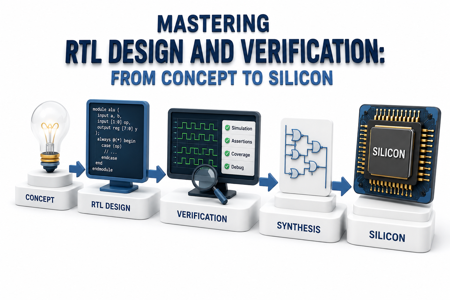
Mastering RTL Design and Verification: From Concept to Silicon
Navigate through this article using the table of contents below
Table of Contents
No headings found in this article.
In today's semiconductor industry, a single design flaw can cost millions of dollars and delay product launches by months. This is why mastering RTL (Register Transfer Level) design and verification has become one of the most critical skills in modern chip development. From AI accelerators and automotive processors to high-performance computing systems and consumer electronics, every successful integrated circuit begins with a robust RTL design and a comprehensive verification strategy. Understanding how to transform a design concept into silicon-ready hardware is essential for engineers aiming to deliver reliable, high-performance, and power-efficient chips.
RTL design and verification form the foundation of the digital IC design flow, ensuring that hardware functionality is accurately implemented and thoroughly validated before fabrication. RTL designers translate system specifications into synthesizable hardware descriptions, while verification engineers use advanced methodologies, simulations, assertions, and coverage-driven techniques to identify and eliminate bugs early in the development cycle. In this blog, we will explore the complete RTL design and verification journey, covering key concepts, industry-standard tools, best practices, and emerging trends that help semiconductor companies achieve first-pass silicon success and accelerate time-to-market.
Introduction to RTL Design and Its Role in Modern Semiconductor Development
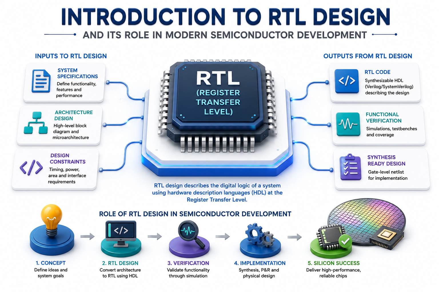
RTL (Register Transfer Level) design is a fundamental stage in the digital integrated circuit (IC) development process, where hardware functionality is described using hardware description languages (HDLs) such as Verilog and SystemVerilog. At this level, designers define how data moves between registers and how logical operations are performed within a digital system. RTL design serves as the bridge between high-level architectural specifications and the physical implementation of semiconductor devices, making it a critical component of ASIC and FPGA development. A well-structured RTL design ensures optimal performance, power efficiency, and scalability while reducing the risk of costly design errors later in the chip development cycle.
In modern semiconductor development, RTL design plays a crucial role in enabling the creation of complex chips used in artificial intelligence, automotive electronics, 5G communication systems, consumer devices, and high-performance computing applications. As semiconductor technologies continue to advance, engineers must develop robust and synthesizable RTL code that can be efficiently verified, synthesized, and implemented in silicon. Combined with comprehensive verification methodologies, RTL design helps ensure that a chip functions according to specifications before fabrication, significantly improving design reliability, reducing time-to-market, and increasing the likelihood of achieving first-pass silicon success.
Understanding the Complete RTL-to-GDSII Design Flow: From Specification to Silicon
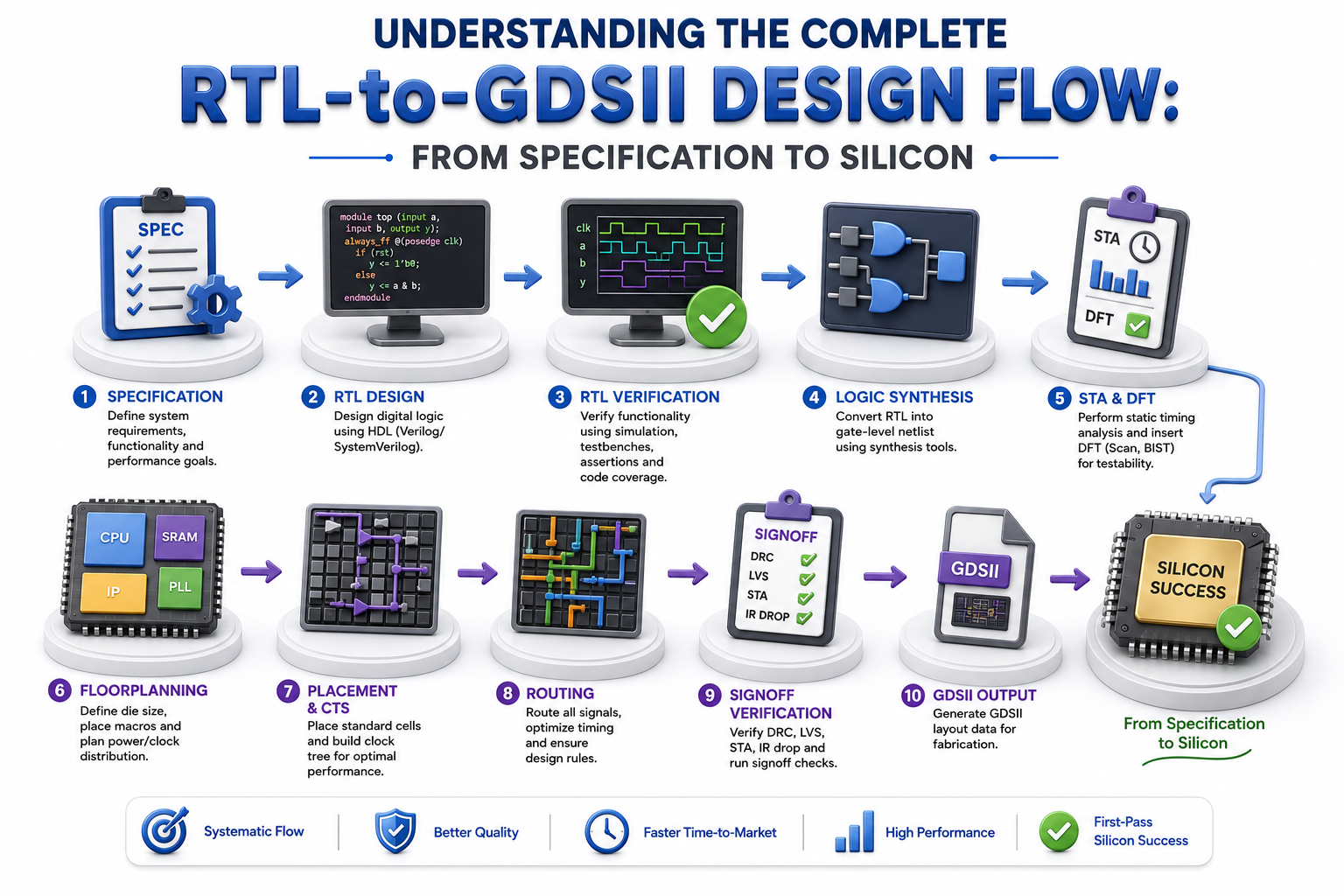
The RTL-to-GDSII design flow is the backbone of modern ASIC development, transforming a product idea into a manufacturable semiconductor chip. The process begins with system specification and architectural design, where engineers define the chip's functionality, performance targets, power requirements, and interface protocols. Based on these specifications, RTL designers create hardware models using languages such as Verilog or SystemVerilog. The RTL code represents the intended hardware behavior and serves as the foundation for all subsequent stages of the design process. At this stage, maintaining coding standards, modularity, and design scalability is essential to ensure efficient development and future design reuse.
Once the RTL design is completed, it undergoes extensive functional verification to confirm that the implementation matches the original specifications. Verification engineers employ simulation, assertion-based verification, coverage analysis, and advanced methodologies such as UVM (Universal Verification Methodology) to identify and eliminate functional bugs. After successful verification, the RTL code is synthesized into a gate-level netlist using Electronic Design Automation (EDA) tools. This netlist is then optimized for timing, area, and power consumption. Additional steps such as Design for Testability (DFT), static timing analysis (STA), formal verification, and equivalence checking are performed to ensure the design is ready for physical implementation.
The final phase of the RTL-to-GDSII flow involves physical design, where the synthesized netlist is transformed into a physical chip layout. This stage includes floorplanning, placement, clock tree synthesis, routing, signal integrity analysis, and physical verification checks such as Design Rule Checking (DRC) and Layout Versus Schematic (LVS). After all design constraints are met and the chip passes signoff verification, the completed layout is generated in GDSII format, the industry-standard file used for semiconductor fabrication. The GDSII file is then sent to the foundry for manufacturing, resulting in silicon chips that can be packaged, tested, and deployed in real-world applications. A well-executed RTL-to-GDSII flow is crucial for achieving high-quality silicon, reducing development costs, and ensuring successful first-pass chip production.
RTL Coding Best Practices for High-Quality ASIC and FPGA Design
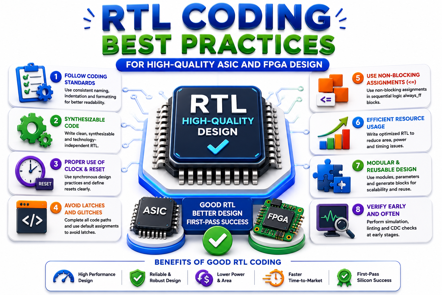
RTL coding best practices are essential for developing reliable, synthesizable, and maintainable ASIC and FPGA designs. High-quality RTL code begins with a clear understanding of design specifications and the use of structured coding methodologies. Engineers should follow consistent naming conventions, modular design principles, and proper code documentation to improve readability and simplify debugging. Writing synthesizable Verilog or SystemVerilog code, avoiding unintended latches, minimizing combinational loops, and using synchronous design techniques are critical practices that help ensure predictable hardware behavior. Additionally, parameterized and reusable RTL modules promote design scalability and reduce development time across multiple projects.
Another important aspect of RTL coding is optimizing designs for performance, power consumption, and silicon area while maintaining functional correctness. Designers should use efficient state machine implementations, proper clock and reset strategies, and timing-aware coding techniques to achieve design goals. Early simulation and linting checks help identify coding errors before they propagate into later stages of the design flow. Furthermore, adhering to industry-standard coding guidelines improves compatibility with synthesis, verification, and static timing analysis tools. By following proven RTL coding best practices, engineers can reduce design iterations, improve verification efficiency, and significantly increase the likelihood of achieving first-pass silicon success in both ASIC and FPGA development projects.
Functional Verification Fundamentals: Simulation, Debugging, and Coverage Analysis
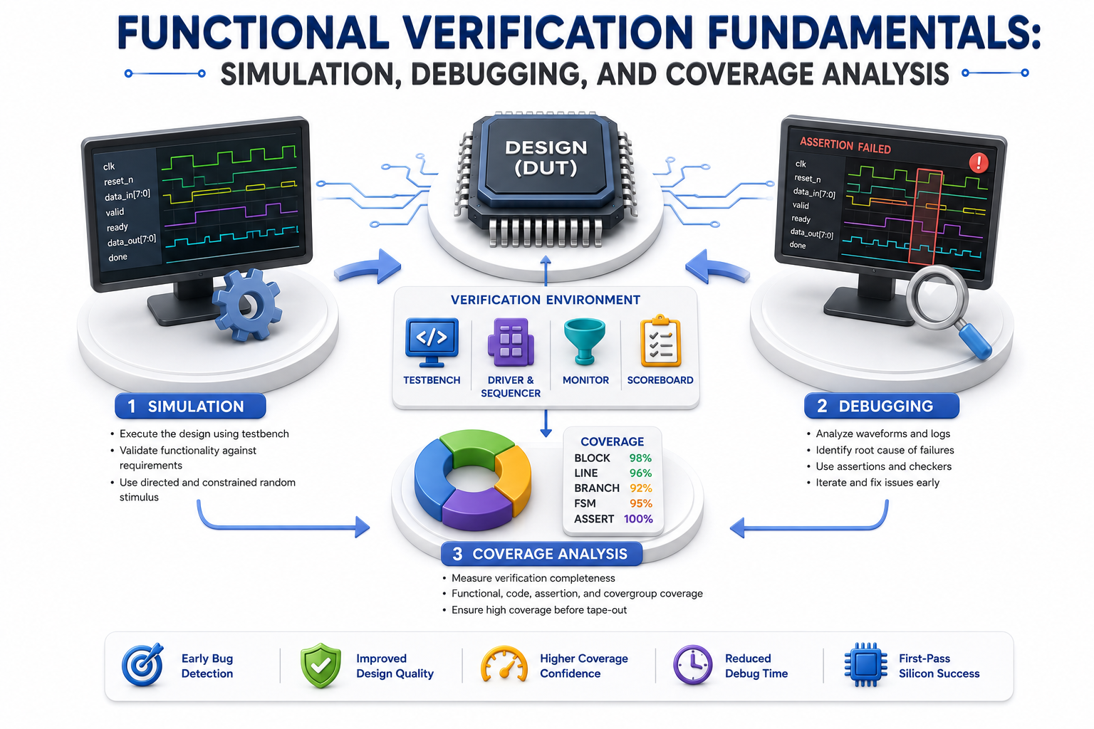
Functional verification is a critical phase of the digital IC design process that ensures an RTL design behaves according to its intended specifications before it is manufactured. Since functional bugs discovered after fabrication can lead to costly silicon re-spins and project delays, verification plays a vital role in reducing development risks. Simulation is one of the most widely used verification techniques, allowing engineers to execute test cases and observe how the design responds under various operating conditions. By creating comprehensive testbenches and applying different input scenarios, verification teams can identify design flaws early and validate that the RTL implementation meets all functional requirements.
Debugging is an essential part of the verification process and involves analyzing simulation results to locate and resolve design issues. Verification engineers use waveform viewers, log analysis tools, assertions, and debugging environments to trace signal activity and pinpoint the root cause of failures. Effective debugging requires a deep understanding of both the design architecture and verification environment. Modern verification methodologies often incorporate automated debugging features and assertion-based verification to accelerate bug detection and improve overall verification productivity. Efficient debugging not only shortens development cycles but also enhances design quality and reliability.
Coverage analysis is used to measure the completeness and effectiveness of the verification effort. It helps engineers determine whether all functional scenarios, design states, and critical code paths have been exercised during simulation. Coverage metrics typically include code coverage, functional coverage, branch coverage, toggle coverage, and assertion coverage. By analyzing coverage reports, verification teams can identify untested areas of the design and develop additional test cases to improve verification confidence. A strong coverage-driven verification strategy ensures that the design has been thoroughly validated, significantly increasing the likelihood of achieving first-pass silicon success and delivering robust semiconductor products.
SystemVerilog and UVM Methodologies for Advanced RTL Verification
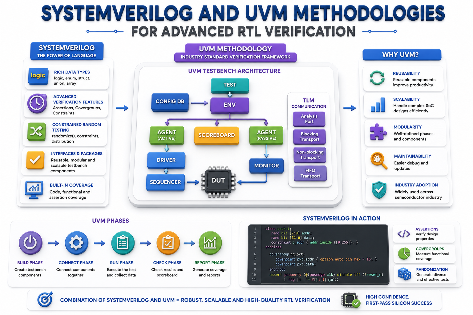
SystemVerilog has become the industry-standard hardware description and verification language for modern semiconductor development, offering powerful features that extend beyond traditional Verilog. It provides advanced capabilities such as object-oriented programming, assertions, constrained-random test generation, interfaces, and functional coverage, making it highly effective for complex RTL verification. Verification engineers use SystemVerilog to build sophisticated testbenches capable of generating diverse test scenarios and validating design behavior under a wide range of operating conditions. These capabilities help improve bug detection, enhance verification quality, and accelerate the overall chip development process.
UVM (Universal Verification Methodology) is a standardized verification framework built on SystemVerilog that enables the creation of reusable, scalable, and modular verification environments. UVM introduces structured components such as drivers, monitors, sequencers, agents, scoreboards, and coverage collectors, allowing verification teams to efficiently verify increasingly complex ASIC and SoC designs. By supporting constrained-random verification, functional coverage, and reusable verification IP (VIP), UVM helps achieve comprehensive design validation while reducing development effort and maintenance costs. Together, SystemVerilog and UVM form the foundation of advanced RTL verification methodologies, enabling semiconductor companies to improve verification efficiency, reduce project risk, and increase the likelihood of first-pass silicon success.
Assertion-Based Verification (ABV) and Formal Verification Techniques
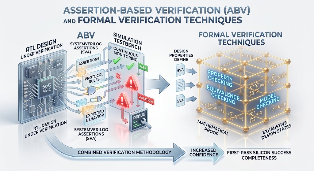
Assertion-Based Verification (ABV) is a powerful verification methodology used to detect design errors early in the RTL development cycle. Assertions are statements written in SystemVerilog Assertions (SVA) or other assertion languages that define expected design behavior, protocol rules, timing requirements, and functional constraints. During simulation, these assertions continuously monitor the design and automatically flag violations whenever the implemented behavior deviates from the specified requirements. By embedding assertions directly into the verification environment, engineers can identify bugs closer to their source, improve debugging efficiency, and enhance overall verification coverage. ABV also promotes better design documentation by explicitly capturing critical design assumptions and requirements.
Formal verification complements simulation-based verification by mathematically proving whether a design satisfies specific properties without requiring test vectors or stimulus generation. Unlike traditional simulation, which can only verify scenarios that are explicitly tested, formal verification exhaustively analyzes all possible design states within defined constraints. Common formal verification techniques include property checking, equivalence checking, and model checking, which help validate protocol compliance, detect corner-case bugs, and ensure RTL-to-netlist consistency. When combined with Assertion-Based Verification, formal verification significantly improves verification completeness, reduces the risk of functional escapes, and increases confidence in achieving first-pass silicon success for complex ASIC and SoC designs.
Common RTL Design and Verification Challenges and How to Overcome Them
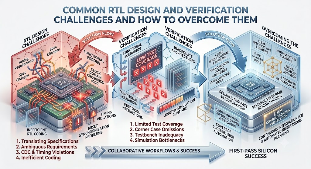
RTL design and verification projects often face numerous challenges as semiconductor devices become increasingly complex. One of the most common RTL design challenges is translating high-level specifications into accurate and synthesizable hardware descriptions. Ambiguous requirements, design complexity, and frequent specification changes can introduce functional errors and inconsistencies early in the development cycle. Additionally, issues such as improper clock domain crossings (CDC), reset synchronization problems, timing violations, and inefficient RTL coding practices can negatively impact design quality and performance. To overcome these challenges, engineering teams should establish clear design specifications, follow standardized coding guidelines, perform regular design reviews, and utilize static analysis tools to detect potential issues early.
Verification complexity presents another significant challenge, particularly for large ASIC and SoC designs containing multiple subsystems and interfaces. Ensuring that every functional scenario, corner case, and protocol interaction is thoroughly validated requires substantial verification effort. Limited test coverage, inadequate testbench architectures, and lengthy simulation runtimes can increase the risk of undetected bugs reaching silicon. To address these issues, verification teams leverage advanced methodologies such as UVM, constrained-random testing, assertion-based verification (ABV), and coverage-driven verification. These techniques improve test quality, automate stimulus generation, and help achieve more comprehensive design validation while reducing manual effort.
Another major challenge is meeting aggressive project schedules while maintaining high design reliability and first-pass silicon success. As tape-out deadlines approach, teams often face pressure to close verification coverage, resolve late-stage bugs, and meet timing, power, and area constraints simultaneously. Poor communication between design and verification teams can further delay project progress and increase debugging complexity. Organizations can overcome these challenges by adopting collaborative workflows, continuous integration practices, automated regression testing, and early verification planning. By combining robust RTL design methodologies with comprehensive verification strategies, engineering teams can reduce development risks, improve productivity, and successfully deliver high-quality semiconductor products within tight market timelines.
Industry-Standard EDA Tools Used in RTL Design and Verification Engineering
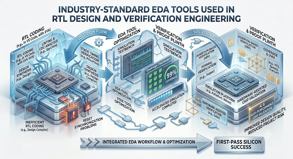
Electronic Design Automation (EDA) tools are essential for modern RTL design and verification engineering, enabling semiconductor companies to develop increasingly complex ASICs, FPGAs, and System-on-Chip (SoC) solutions efficiently. During the RTL design phase, engineers rely on industry-standard tools for coding, synthesis, linting, clock domain crossing (CDC) analysis, and static timing verification. Popular EDA solutions from leading vendors support RTL development by helping designers identify coding issues, optimize hardware implementation, and ensure compliance with design specifications. These tools automate critical tasks, improve design productivity, and reduce the likelihood of errors propagating into later stages of the chip development cycle.
In the verification domain, advanced EDA tools provide powerful capabilities for simulation, debugging, assertion-based verification, formal verification, coverage analysis, and UVM-based verification environments. Engineers use these tools to validate design functionality, analyze waveform activity, measure verification completeness, and detect complex bugs before tape-out. Modern verification platforms also support accelerated simulation, emulation, and hardware-assisted verification to manage the growing complexity of AI, automotive, networking, and high-performance computing chips. By leveraging industry-standard EDA tools throughout the RTL design and verification flow, organizations can improve design quality, shorten development cycles, reduce project risks, and significantly increase the chances of achieving first-pass silicon success.
Achieving First-Pass Silicon Success Through Effective Verification Strategies
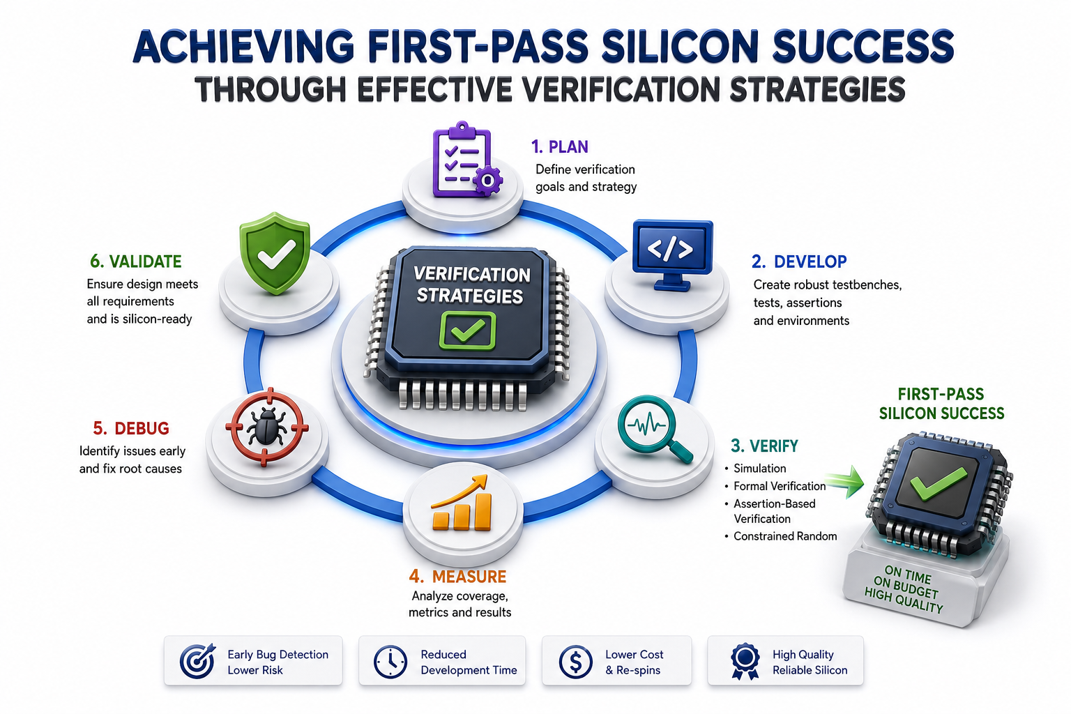
Achieving first-pass silicon success is one of the primary objectives in semiconductor product development, as it ensures that a chip functions correctly after fabrication without requiring costly redesigns or silicon re-spins. Since manufacturing advanced semiconductor devices involves significant time and financial investment, identifying and eliminating design bugs before tape-out is critical. Effective verification strategies help validate the functionality, performance, and reliability of RTL designs throughout the development cycle. By establishing a comprehensive verification plan early in the project, engineering teams can systematically verify design requirements and reduce the risk of functional defects reaching silicon.
A robust verification strategy combines multiple techniques, including simulation-based verification, constrained-random testing, assertion-based verification (ABV), formal verification, and coverage-driven methodologies. Advanced frameworks such as UVM enable the creation of reusable and scalable verification environments capable of testing a wide range of functional scenarios and corner cases. Functional coverage metrics help engineers measure verification completeness, while assertions and formal methods provide additional confidence by validating critical design properties and protocol compliance. Together, these approaches improve bug detection efficiency and significantly enhance design quality before fabrication.
Collaboration between RTL designers and verification engineers is equally important for achieving first-pass silicon success. Continuous regression testing, automated verification workflows, design reviews, and early bug tracking help identify issues before they become difficult and expensive to fix. Additionally, verifying timing, power, clock domain crossings, reset behavior, and design-for-testability requirements ensures that both functional and implementation-related challenges are addressed before tape-out. By adopting a comprehensive and disciplined verification methodology, semiconductor organizations can reduce development risks, accelerate time-to-market, lower overall project costs, and maximize the probability of delivering high-quality silicon on the first manufacturing run.
Future Trends in RTL Design and Verification for AI, Automotive, and High-Performance Computing Chips

The future of RTL design and verification is being shaped by the rapid growth of artificial intelligence (AI), automotive electronics, and high-performance computing (HPC) applications, all of which demand increasingly complex and performance-driven semiconductor devices. AI accelerators and HPC processors require massive parallelism, high bandwidth, and energy-efficient architectures, driving the need for more sophisticated RTL design methodologies. At the same time, automotive systems such as Advanced Driver Assistance Systems (ADAS), autonomous vehicles, and functional safety applications require extremely reliable hardware that complies with stringent industry standards. As chip complexity continues to increase, engineers are adopting advanced design automation techniques, reusable IP-based design approaches, and scalable verification methodologies to manage development challenges more effectively.
Emerging trends in verification include the integration of artificial intelligence and machine learning to automate test generation, bug prediction, coverage closure, and regression analysis. Formal verification, emulation, FPGA prototyping, and hardware-assisted verification platforms are also becoming increasingly important for validating large System-on-Chip (SoC) designs within tight development schedules. Additionally, safety-critical automotive chips are driving greater adoption of functional safety verification standards and fault-injection testing techniques. As the semiconductor industry moves toward heterogeneous computing, chiplet-based architectures, and advanced process technologies, RTL design and verification engineers will need to leverage intelligent automation, advanced EDA tools, and next-generation verification strategies to ensure faster development cycles, higher design quality, and successful first-pass silicon implementation.
Conclusion
Mastering RTL design and verification is essential for transforming innovative semiconductor concepts into reliable, high-performance silicon. From developing synthesizable RTL code and implementing robust design methodologies to applying advanced verification techniques such as simulation, UVM, assertion-based verification, and formal verification, every stage plays a critical role in ensuring design correctness. A well-structured RTL-to-silicon flow helps engineering teams detect and resolve issues early, minimize development risks, and significantly improve the chances of achieving first-pass silicon success.
As semiconductor technologies continue to evolve to support AI, automotive, 5G, and high-performance computing applications, the importance of efficient RTL design and comprehensive verification strategies will only grow. Engineers who understand the complete design and verification lifecycle, leverage industry-standard EDA tools, and adopt emerging verification technologies will be better equipped to tackle increasing design complexity. By combining strong technical expertise with proven best practices, organizations can accelerate time-to-market, reduce costly silicon re-spins, and deliver next-generation chips that meet the demanding requirements of modern electronic systems.