
RTL Design vs. RTL Verification: Key Differences and Best Practices
Navigate through this article using the table of contents below
Table of Contents
No headings found in this article.
Did you know that even the most advanced semiconductor chips can fail if there is a gap between RTL design and RTL verification? In today's competitive semiconductor industry, achieving first-pass silicon success is critical, making both RTL Design and RTL Verification indispensable stages of the VLSI development cycle. While RTL designers focus on translating system specifications into synthesizable hardware descriptions, RTL verification engineers ensure that the design functions correctly under all possible scenarios before fabrication. Understanding the differences between these two domains is essential for engineers, students, and organizations aiming to develop reliable and high-performance integrated circuits.
RTL Design vs. RTL Verification is one of the most discussed topics in modern chip development because both disciplines work together to reduce costly design errors, improve product quality, and accelerate time-to-market. RTL design primarily involves coding digital circuits using hardware description languages such as Verilog and SystemVerilog, whereas RTL verification uses advanced methodologies, simulation techniques, assertions, and coverage-driven approaches to validate design correctness. In this article, we will explore the key differences between RTL Design and RTL Verification, their responsibilities, required skill sets, and the best practices that help semiconductor companies deliver robust ASIC and FPGA solutions successfully.
Understanding RTL Design and RTL Verification in Modern VLSI Development
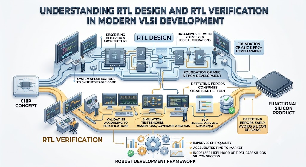
RTL (Register Transfer Level) Design and RTL Verification are two fundamental pillars of modern VLSI development that work together to transform a chip concept into a functional silicon product. RTL Design involves describing the behavior and architecture of digital circuits using hardware description languages such as Verilog and SystemVerilog. RTL designers convert system specifications into synthesizable code that defines how data moves between registers and how logical operations are performed within the hardware. This stage serves as the foundation of ASIC and FPGA development, ensuring that the intended functionality is accurately represented before moving to synthesis, implementation, and fabrication.
RTL Verification focuses on validating that the RTL design behaves according to the specified requirements under all possible operating conditions. Verification engineers use simulation, testbenches, assertions, coverage analysis, and advanced methodologies such as UVM (Universal Verification Methodology) to identify functional bugs before the design reaches silicon. In modern VLSI development, verification often consumes a significant portion of the overall project effort because detecting errors early helps avoid costly silicon re-spins and project delays. Together, RTL Design and RTL Verification create a robust development framework that improves chip quality, accelerates time-to-market, and increases the likelihood of achieving first-pass silicon success.
Key Objectives of RTL Design vs. RTL Verification
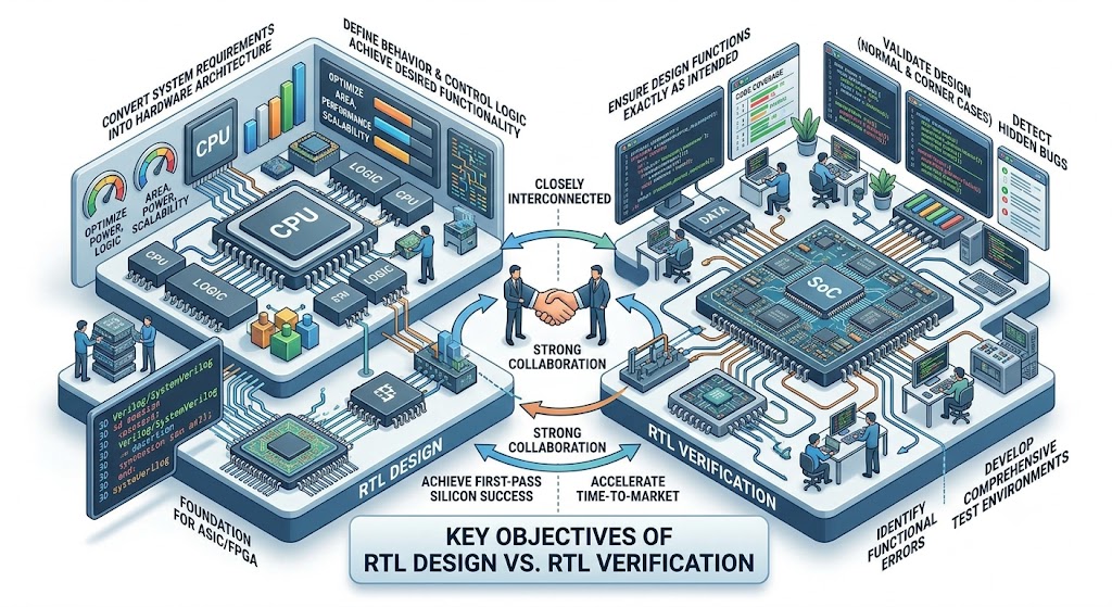
The primary objective of RTL Design is to convert system-level requirements into a hardware architecture that can be implemented efficiently on silicon. RTL designers create synthesizable code using languages such as Verilog and SystemVerilog to define the behavior, data flow, and control logic of digital circuits. Their focus is on achieving the desired functionality while optimizing important design parameters such as area, power consumption, performance, and scalability. A well-structured RTL design serves as the foundation for successful ASIC and FPGA development and directly impacts the overall quality of the final chip.
In contrast, the main objective of RTL Verification is to ensure that the RTL design functions exactly as intended according to the design specifications. Verification engineers develop comprehensive test environments, create test cases, write assertions, and perform coverage analysis to identify functional errors before fabrication. The goal is to validate the design under both normal and corner-case scenarios, ensuring that all features operate correctly and that hidden bugs are detected early in the development cycle. Effective RTL verification significantly reduces the risk of costly silicon failures and re-spins.
Although RTL Design and RTL Verification have different objectives, they are closely interconnected throughout the VLSI design flow. RTL designers focus on building reliable hardware logic, while verification engineers concentrate on proving its correctness and robustness. Together, these disciplines help semiconductor companies achieve first-pass silicon success, improve product reliability, and accelerate time-to-market. A strong collaboration between design and verification teams ensures that complex SoCs, ASICs, and FPGA-based systems meet performance targets while maintaining high functional quality and verification coverage.
Roles and Responsibilities of RTL Design Engineers and Verification Engineers
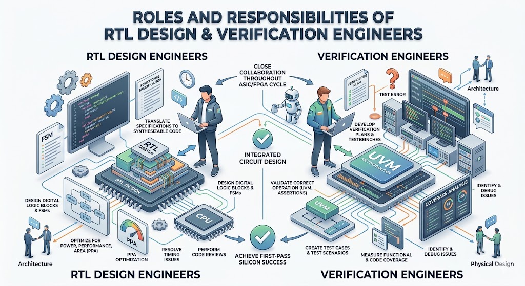
RTL Design Engineers are responsible for translating functional specifications into synthesizable hardware descriptions using languages such as Verilog and SystemVerilog. Their key responsibilities include designing digital logic blocks, developing finite state machines, creating data-path architectures, optimizing designs for power, performance, and area (PPA), and ensuring compliance with project requirements. They also perform code reviews, analyze synthesis reports, resolve timing-related issues, and collaborate with architecture, physical design, and verification teams throughout the ASIC or FPGA development cycle. The quality of the RTL code produced by design engineers directly influences the efficiency, scalability, and reliability of the final semiconductor product.
Verification Engineers focus on validating that the RTL design operates correctly under all intended conditions before silicon fabrication. Their responsibilities include developing verification plans, creating testbenches, writing test cases, implementing assertions, performing simulation-based testing, and measuring functional and code coverage. Using advanced methodologies such as UVM (Universal Verification Methodology), they systematically identify and debug design issues, ensuring that all functional requirements are met. Verification engineers work closely with RTL designers to reproduce, analyze, and resolve bugs, helping organizations reduce design risks, prevent costly silicon re-spins, and achieve first-pass silicon success in modern VLSI projects.
Essential Skills Required for RTL Design and RTL Verification Careers
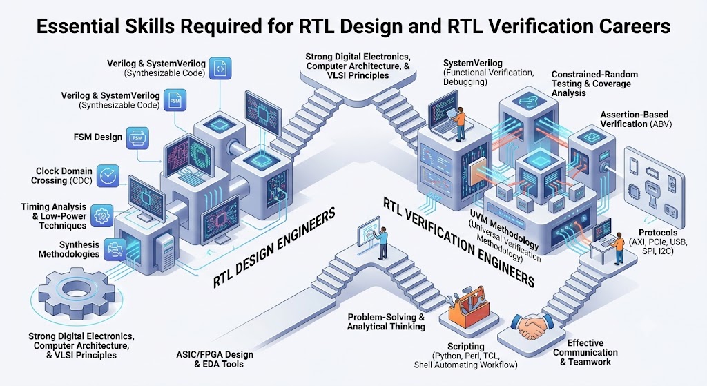
A successful career in RTL Design requires a strong foundation in digital electronics, computer architecture, and VLSI design principles. RTL Design Engineers must be proficient in hardware description languages such as Verilog and SystemVerilog to create synthesizable and efficient digital circuits. They should also understand finite state machine (FSM) design, clock domain crossing (CDC) concepts, timing analysis, low-power design techniques, and synthesis methodologies. Familiarity with ASIC and FPGA design flows, along with hands-on experience using industry-standard EDA tools, is essential for developing high-performance and reliable hardware solutions.
For RTL Verification careers, engineers need expertise in functional verification methodologies and debugging techniques. Strong knowledge of SystemVerilog, assertion-based verification (ABV), constrained-random testing, coverage analysis, and testbench development is highly valuable. Verification professionals are also expected to be skilled in Universal Verification Methodology (UVM), which has become the industry standard for building scalable and reusable verification environments. Additionally, understanding protocols such as AXI, PCIe, USB, SPI, and I2C helps verification engineers validate complex SoC and IP designs more effectively.
Both RTL Design and RTL Verification professionals benefit from strong problem-solving, analytical thinking, and scripting skills. Knowledge of programming languages such as Python, Perl, TCL, or Shell scripting helps automate repetitive tasks, improve productivity, and streamline verification workflows. Effective communication and teamwork are equally important, as design and verification teams must collaborate closely to identify and resolve issues throughout the VLSI development process. By mastering these technical and professional skills, engineers can build successful careers in ASIC design, FPGA development, and advanced semiconductor product engineering.
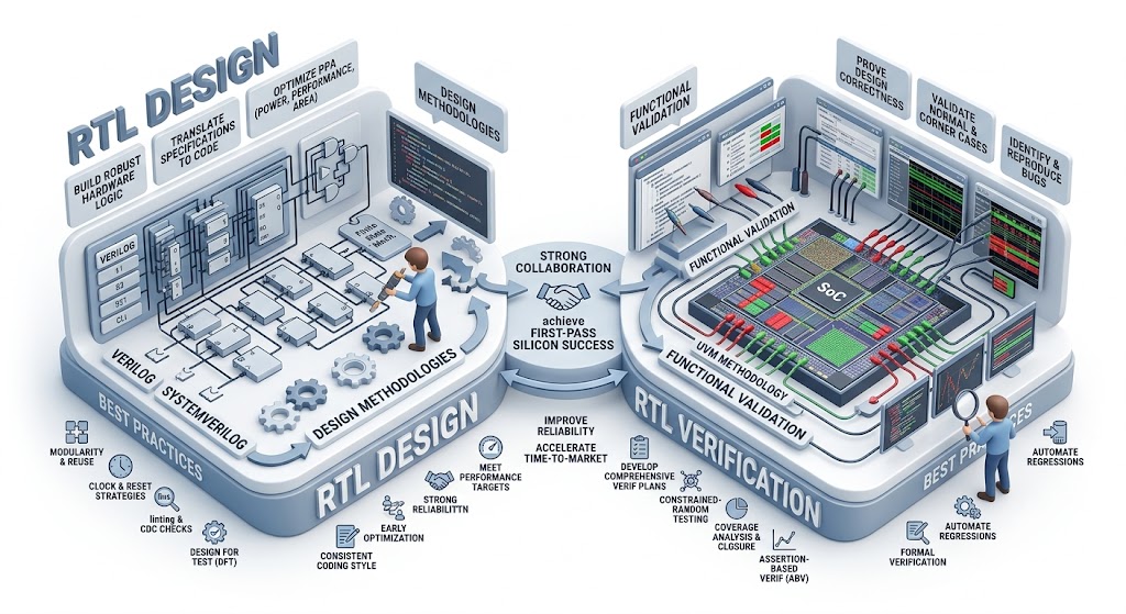
RTL Coding Practices and Design Methodologies for High-Quality Hardware Development
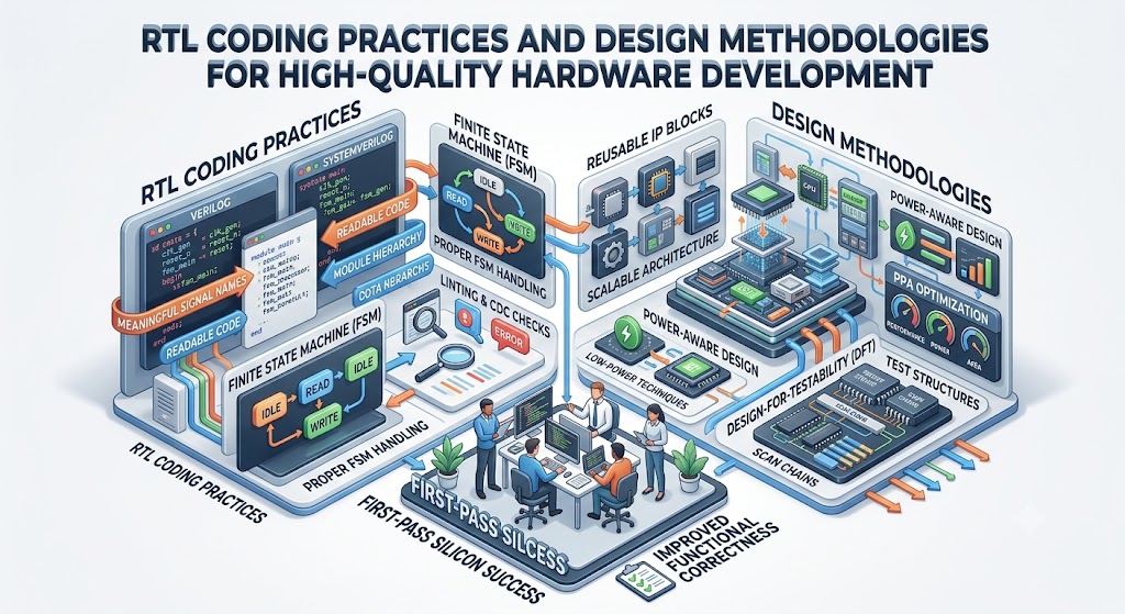
High-quality hardware development begins with adopting robust RTL coding practices that improve design readability, maintainability, and synthesis efficiency. RTL designers should follow standardized coding guidelines, use meaningful signal names, maintain modular design structures, and write synthesizable Verilog or SystemVerilog code that is easy to understand and debug. Proper handling of clocking schemes, reset strategies, finite state machines (FSMs), and clock domain crossings (CDCs) is essential for preventing functional and timing-related issues. Consistent code reviews, linting checks, and adherence to design standards help reduce errors early in the development cycle and improve overall design quality.
Effective RTL design methodologies focus on creating scalable, reusable, and verification-friendly hardware architectures. Designers often use hierarchical design approaches, parameterized modules, and reusable IP blocks to simplify complex ASIC and FPGA projects. Design-for-testability (DFT) considerations, power-aware design techniques, and early verification planning are also important components of modern hardware development. By combining structured RTL coding practices with proven design methodologies, semiconductor teams can accelerate development, improve functional correctness, optimize power-performance-area (PPA) metrics, and increase the likelihood of achieving first-pass silicon success in advanced VLSI designs.
Functional Verification Techniques: Simulation, Assertions, and Coverage Analysis
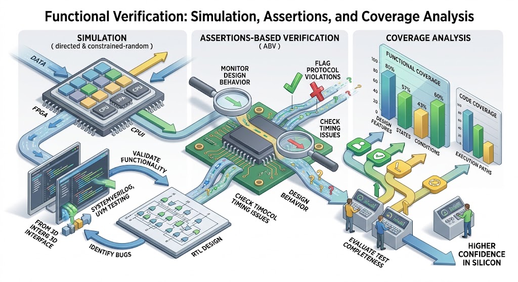
Functional verification is a critical stage in the VLSI design flow that ensures an RTL design operates according to its specifications before silicon fabrication. Simulation is one of the most widely used verification techniques, allowing engineers to execute test cases and observe the behavior of digital circuits under various operating conditions. Through directed and constrained-random testing, verification teams can validate functionality, identify design bugs, and analyze system responses to both normal and corner-case scenarios. Advanced simulation environments built using SystemVerilog and UVM help improve verification efficiency and enable comprehensive testing of complex ASIC and FPGA designs.
Assertions and coverage analysis further strengthen the verification process by providing automated mechanisms to detect errors and measure verification completeness. Assertion-Based Verification (ABV) uses SystemVerilog Assertions (SVA) to continuously monitor design behavior and flag protocol violations, timing issues, or unexpected conditions during simulation. Coverage analysis, including functional coverage and code coverage, helps engineers evaluate whether all design features, states, conditions, and execution paths have been adequately tested. By combining simulation, assertions, and coverage-driven verification, organizations can improve design quality, reduce the risk of silicon failures, and achieve higher confidence in the functionality and reliability of modern semiconductor devices.
Common Challenges in RTL Design and Verification Processes
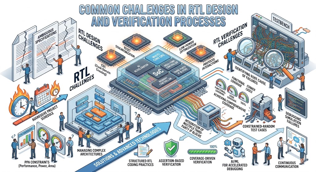
RTL Design and RTL Verification teams face numerous challenges as semiconductor devices continue to grow in complexity. One of the most common issues is dealing with incomplete or ambiguous design specifications, which can lead to misunderstandings during implementation and verification. As modern ASICs, FPGAs, and SoCs integrate billions of transistors and multiple subsystems, designers must manage complex architectures while ensuring that performance, power consumption, and area constraints are met. Maintaining design quality while adhering to aggressive project schedules adds further pressure to the development process.
Another major challenge in RTL verification is achieving comprehensive verification coverage. Verification engineers must ensure that all functional scenarios, corner cases, and protocol interactions are thoroughly tested before tape-out. Creating effective testbenches, developing constrained-random test cases, debugging simulation failures, and closing functional and code coverage gaps can be highly time-consuming. Additionally, identifying the root cause of failures often requires close collaboration between design and verification teams, especially when bugs are difficult to reproduce or occur only under specific operating conditions.
The increasing adoption of advanced technologies such as AI accelerators, high-performance computing processors, and automotive SoCs introduces additional verification complexity. Challenges such as clock domain crossings (CDC), reset synchronization, low-power verification, and integration of multiple third-party IP blocks require specialized expertise and sophisticated verification methodologies. To overcome these obstacles, organizations rely on structured RTL coding practices, assertion-based verification, coverage-driven verification, automation tools, and continuous communication between engineering teams. Addressing these challenges effectively helps reduce project risks, prevent costly silicon re-spins, and improve overall product reliability.
Future Trends in RTL Design and Verification for AI, Automotive, and High-Performance Computing Chips
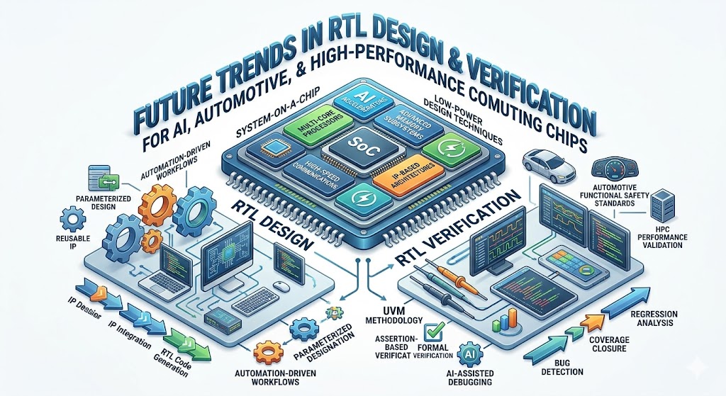
The future of RTL Design and RTL Verification is being shaped by the rapid growth of artificial intelligence (AI), automotive electronics, and high-performance computing (HPC) applications. Modern chips are becoming significantly more complex, integrating AI accelerators, multi-core processors, advanced memory subsystems, and high-speed communication interfaces on a single SoC. As a result, RTL designers are increasingly adopting reusable IP-based architectures, parameterized design methodologies, and automation-driven workflows to improve productivity and manage design complexity. The growing demand for energy-efficient computing is also driving innovation in low-power RTL design techniques, enabling semiconductor companies to develop high-performance chips that meet stringent power and thermal requirements.
On the verification side, advanced methodologies such as UVM, assertion-based verification, formal verification, and AI-assisted debugging are becoming essential for validating next-generation semiconductor devices. Automotive chips require rigorous verification to comply with functional safety standards and ensure reliable operation in safety-critical environments, while AI and HPC processors demand extensive testing to verify performance, scalability, and data integrity. Machine learning-powered verification tools are expected to accelerate bug detection, coverage closure, and regression analysis, helping engineering teams reduce development cycles and improve verification efficiency. As chip complexity continues to increase, the collaboration between RTL Design and RTL Verification teams will become even more critical for achieving first-pass silicon success and delivering reliable, high-quality semiconductor products.
Conclusion
RTL Design and RTL Verification are two closely connected disciplines that play a vital role in the successful development of modern semiconductor devices. While RTL Design focuses on creating efficient and synthesizable hardware architectures, RTL Verification ensures that these designs function correctly and meet all specified requirements before fabrication. Understanding the key differences between RTL Design and RTL Verification helps engineers appreciate how both domains contribute to reducing design risks, improving chip quality, and achieving first-pass silicon success. Together, they form the foundation of reliable ASIC, FPGA, and SoC development in today's highly competitive semiconductor industry.
As chip complexity continues to increase with advancements in AI, automotive electronics, 5G, and high-performance computing, the importance of robust RTL coding practices and comprehensive verification methodologies has never been greater. Organizations that invest in strong collaboration between design and verification teams, adopt industry-standard tools such as SystemVerilog and UVM, and follow proven best practices are better positioned to deliver high-quality products faster and more efficiently. By mastering both RTL Design and RTL Verification concepts, professionals can build successful careers while helping drive innovation in the next generation of semiconductor technologies.