
RTL Design vs Verification: Understanding the Two Pillars of Digital IC Design
Navigate through this article using the table of contents below
Table of Contents
No headings found in this article.
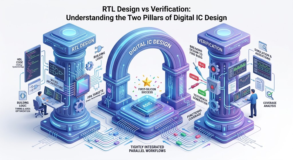
In today’s rapidly evolving semiconductor industry, the success of any digital chip depends heavily on two fundamental disciplines—RTL Design and Verification. These two pillars of digital IC design form the backbone of modern ASIC and FPGA development, ensuring that complex integrated circuits not only function as intended but also meet strict performance, power, and reliability requirements. As chip complexity continues to grow with advanced AI, automotive, and high-performance computing applications, understanding the distinction and synergy between RTL Design and Verification has become more critical than ever.
RTL Design focuses on implementing the intended hardware functionality using Hardware Description Languages (HDLs) like Verilog or SystemVerilog, translating architectural specifications into synthesizable logic. On the other hand, Verification ensures that the designed RTL behaves correctly under all possible conditions by applying rigorous simulation, testbenches, and formal verification techniques. Together, RTL Design and Verification play a crucial role in achieving first-silicon success, reducing costly design iterations, and delivering robust, production-ready digital systems.
Introduction to RTL Design and Verification in Digital IC Design Flow
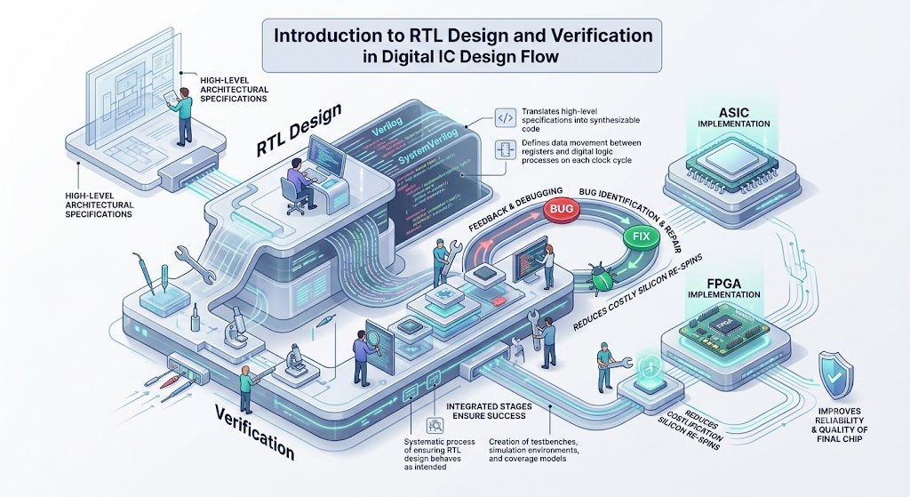
RTL Design and Verification form the foundation of the modern digital IC design flow, acting as two tightly integrated stages that ensure the successful development of complex semiconductor chips. Register Transfer Level (RTL) Design represents the phase where high-level architectural specifications are translated into synthesizable hardware description code, typically using languages like Verilog or SystemVerilog. This stage defines how data moves between registers and how the digital logic processes it on each clock cycle, making it a critical step in determining the functionality, performance, and efficiency of the final chip.
Verification, on the other hand, is the systematic process of ensuring that the RTL design behaves exactly as intended under all possible conditions. It involves the creation of testbenches, simulation environments, and coverage models to detect functional errors early in the design cycle. In the overall digital IC design flow, RTL Design and Verification work in parallel—while RTL focuses on building the logic, Verification continuously validates it. This close interaction helps identify bugs early, reduce costly silicon re-spins, and significantly improve the reliability and quality of ASIC and FPGA implementations.
What is RTL Design? Role in ASIC and FPGA Development
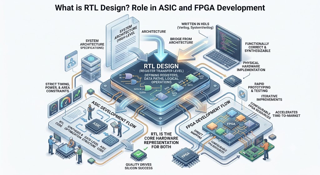
RTL Design (Register Transfer Level Design) is a key stage in the digital IC design flow where a hardware system is described in terms of registers, data paths, and the logical operations performed on data between clock cycles. It is typically written using Hardware Description Languages (HDLs) such as Verilog or SystemVerilog and represents a bridge between high-level architecture and physical hardware implementation. At this level, designers focus on defining the exact behavior of digital circuits in a way that is both functionally correct and synthesizable into real silicon.
In ASIC development, RTL Design plays a critical role in transforming architectural specifications into a gate-level structure that can be synthesized, optimized, and fabricated. Designers ensure that the RTL code meets strict constraints related to timing, power, and area, which are essential for producing efficient and high-performance chips. Any mistakes at this stage can propagate through the entire flow, making RTL quality a major determinant of silicon success.
In FPGA development, RTL Design is directly mapped onto configurable hardware resources within the FPGA fabric. Unlike ASICs, where design is permanently fabricated, FPGA-based RTL implementations allow rapid prototyping, testing, and iterative improvements. This makes RTL Design especially important for validating functionality, optimizing performance, and accelerating time-to-market. In both ASIC and FPGA flows, RTL serves as the core representation of hardware logic that drives the entire implementation process.
What is Verification in VLSI? Importance in Bug-Free Chip Design
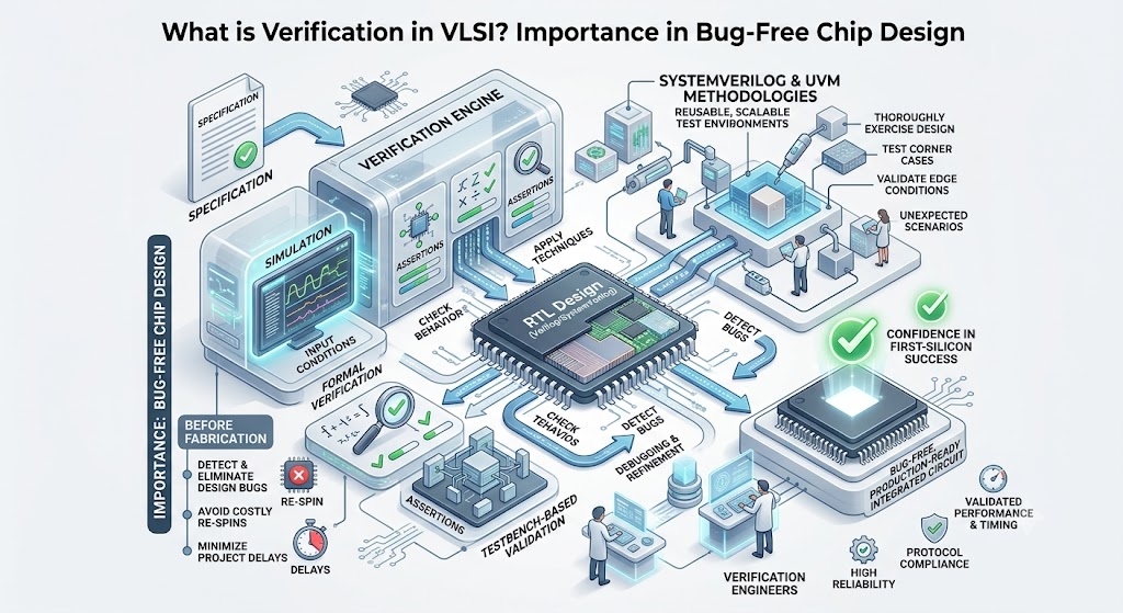
Verification in VLSI is the process of ensuring that a digital design (typically written at the RTL level) correctly implements the intended functionality as defined in the architectural and design specifications. It involves applying a wide range of techniques such as simulation, formal verification, assertions, and testbench-based validation to check whether the design behaves correctly under all possible input conditions. Since modern chips contain billions of transistors and extremely complex logic, verification has become one of the most critical and resource-intensive phases in the VLSI design flow.
The primary importance of verification lies in detecting and eliminating design bugs before the chip is fabricated. Any functional error that escapes into silicon can lead to costly re-spins, project delays, and performance failures in real-world applications. Verification engineers use methodologies like SystemVerilog and UVM (Universal Verification Methodology) to build reusable and scalable test environments that thoroughly exercise the RTL design. This ensures that corner cases, edge conditions, and unexpected scenarios are properly tested and validated.
In bug-free chip design, verification acts as a quality gate that significantly reduces risk and improves reliability. It not only confirms functional correctness but also helps validate performance, timing assumptions, and protocol compliance in complex SoC designs. By identifying issues early in the development cycle, verification minimizes downstream errors and ensures higher confidence in first-silicon success. In modern semiconductor development, strong verification practices are essential for delivering robust, high-performance, and production-ready integrated circuits.
Key Differences Between RTL Design and Verification in Semiconductor Engineering
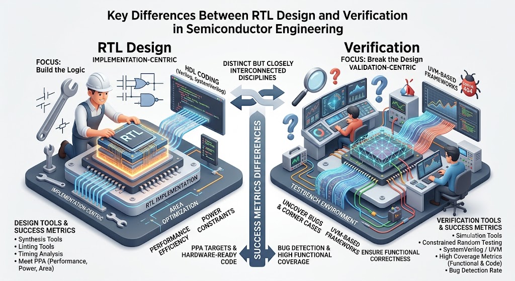
RTL Design and Verification are two distinct but closely interconnected disciplines in semiconductor engineering, each serving a different purpose within the digital IC design flow. RTL Design focuses on implementing the functional logic of a system using Hardware Description Languages (HDLs) such as Verilog or SystemVerilog. It defines how data flows between registers and how digital operations are executed at every clock cycle. In contrast, Verification focuses on validating that the implemented RTL design correctly matches the intended specification and behaves as expected under all possible scenarios.
One of the key differences lies in their objectives and mindset. RTL designers follow a “build the logic” approach, concentrating on efficiency, performance, area optimization, and power constraints to create synthesizable hardware. Verification engineers, however, adopt a “break the design” approach, where the goal is to uncover bugs, corner cases, and unexpected behaviors using techniques like constrained random testing, simulation, assertions, and coverage analysis. While RTL Design is implementation-centric, Verification is validation-centric, ensuring that the implementation is correct before fabrication.
Another major difference is their tools, methodologies, and success metrics. RTL Design primarily uses synthesis tools, linting, and timing analysis tools to ensure the code is hardware-ready. Verification relies heavily on testbench environments, simulation tools, SystemVerilog, and UVM-based frameworks to achieve high functional and code coverage. Success in RTL Design is measured by meeting performance, timing, and area targets, whereas success in Verification is measured by coverage metrics, bug detection rate, and confidence in functional correctness. Together, both roles ensure the delivery of reliable and production-ready semiconductor chips.
RTL Design Methodology: From Specification to Synthesizable Code
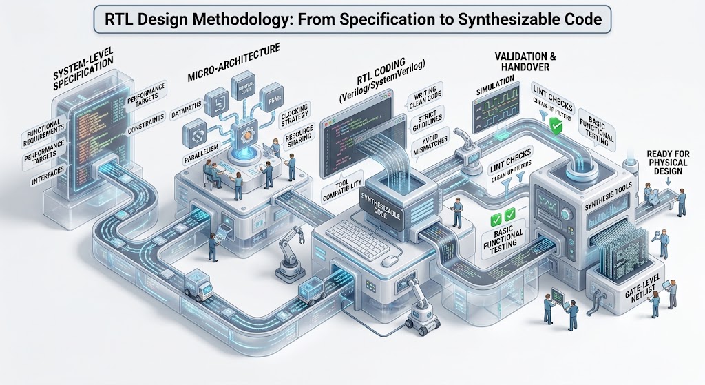
RTL Design methodology begins with a clear understanding of the system-level specification, where functional requirements, performance targets, interfaces, and constraints are defined. This specification is then translated into a micro-architecture, which breaks down the system into smaller functional blocks such as datapaths, control logic, and finite state machines (FSMs). At this stage, design engineers make critical decisions related to pipelining, parallelism, clocking strategy, and resource sharing to ensure the design meets timing, area, and power objectives in ASIC or FPGA implementations.
Once the micro-architecture is finalized, the next step is RTL coding using Hardware Description Languages such as Verilog or SystemVerilog. The focus here is to write clean, synthesizable code that accurately represents the intended hardware behavior at the register transfer level. Designers follow strict coding guidelines to avoid simulation-synthesis mismatches and ensure tool compatibility. After coding, the RTL is validated through simulation, lint checks, and basic functional testing before being handed over to synthesis tools, which convert the RTL into a gate-level netlist ready for physical design. This structured methodology ensures a smooth transition from abstract specification to hardware-realizable implementation.
Functional Verification Techniques: Simulation, Testbenches, and Coverage Analysis
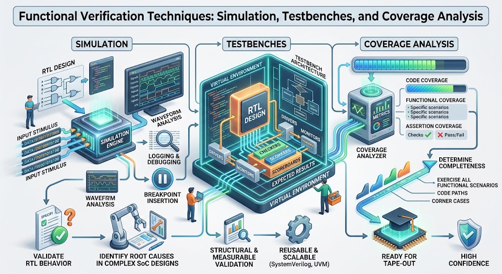
Functional verification in digital IC design relies heavily on simulation as the primary technique to validate RTL behavior before silicon fabrication. Simulation involves executing the RTL design using a set of carefully crafted input stimulus to observe and analyze its output response under different operating conditions. This helps verify whether the design adheres to the original specification. Advanced simulation environments also support debug capabilities such as waveform analysis, logging, and breakpoint insertion, making it easier for verification engineers to trace functional issues and identify root causes in complex SoC designs.
Testbenches and coverage analysis further strengthen the verification process by enabling structured and measurable validation. A testbench acts as a virtual environment that drives stimulus into the RTL design and checks its responses automatically using checkers and scoreboards. Modern methodologies like SystemVerilog and UVM allow reusable and scalable testbench architectures for complex verification projects. Coverage analysis, on the other hand, ensures that all functional scenarios, code paths, and corner cases are exercised during simulation. Metrics such as code coverage, functional coverage, and assertion coverage help determine verification completeness, ensuring that the design is thoroughly validated and ready for tape-out with high confidence.
SystemVerilog and UVM in Modern Verification Methodologies

SystemVerilog has become the industry-standard hardware verification language in modern VLSI design, extending traditional Verilog with powerful constructs specifically tailored for verification tasks. It introduces advanced features such as constrained randomization, assertions, interfaces, classes, and functional coverage, which enable engineers to build highly robust and flexible verification environments. These capabilities allow verification teams to model complex scenarios and systematically explore a wide range of input conditions, significantly improving the probability of detecting hidden design bugs early in the development cycle.
Building on SystemVerilog, the Universal Verification Methodology (UVM) provides a standardized, reusable, and scalable framework for verifying complex digital designs, especially in large System-on-Chip (SoC) environments. UVM is based on object-oriented principles and promotes modular testbench architecture using components such as drivers, monitors, sequencers, scoreboards, and agents. This structure helps engineers create reusable verification IP (VIP), reducing development time and improving consistency across projects. UVM also supports advanced stimulus generation and functional coverage collection, making it highly effective for exhaustive design validation.
Together, SystemVerilog and UVM form the backbone of modern functional verification methodologies in the semiconductor industry. They enable teams to handle the increasing complexity of designs used in AI chips, automotive systems, and high-performance computing devices. By combining powerful language features with a structured verification framework, engineers can achieve higher coverage, faster debug cycles, and greater confidence in first-silicon success. As a result, SystemVerilog and UVM are now essential skills for any professional working in RTL verification and advanced chip design.
Common Challenges in RTL Design and Verification Processes
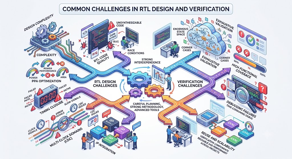
RTL Design and Verification processes in modern semiconductor engineering face several significant challenges due to increasing design complexity and shrinking time-to-market requirements. In RTL Design, engineers must ensure that the code is not only functionally correct but also optimized for power, performance, and area (PPA). Managing timing closure, avoiding race conditions, and ensuring synthesizability across different EDA tools can be difficult, especially in large SoC designs. Additionally, handling multiple clock domains (CDC issues) and integrating third-party IP blocks further increases design complexity and the risk of functional mismatches.
On the verification side, the challenges are even more pronounced due to the need for exhaustive validation of all possible scenarios. Achieving high functional and code coverage is difficult because modern chips have an enormous number of states and corner cases. Debugging failures in large simulation environments can also be time-consuming, as bugs may originate from subtle RTL issues or incorrect assumptions in the testbench. Moreover, ensuring reuse of verification components across projects while maintaining scalability and performance adds another layer of complexity. These challenges make RTL Design and Verification highly interdependent disciplines that require careful planning, strong methodology, and advanced tools to ensure first-silicon success.
Best Practices to Achieve First-Pass Silicon Success in IC Design
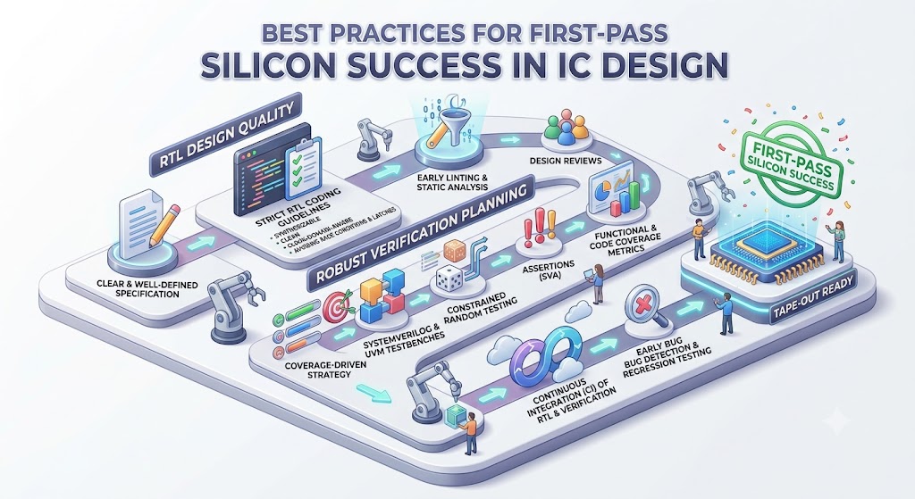
Achieving first-pass silicon success in IC design requires a disciplined approach to RTL design quality and robust verification planning from the earliest stages of the project. One of the most critical best practices is to ensure a clear and well-defined specification before RTL development begins, minimizing ambiguity and design rework. Designers should follow strict RTL coding guidelines, focusing on synthesizable, clean, and clock-domain-aware implementations while avoiding common pitfalls such as race conditions and unintended latches. Early adoption of linting tools, static analysis, and design reviews also helps catch structural and functional issues before they propagate into downstream stages.
On the verification side, a comprehensive and coverage-driven strategy is essential to ensure design correctness under all operating conditions. Using advanced methodologies such as SystemVerilog and UVM enables reusable, scalable, and modular testbenches that can thoroughly exercise the design. Incorporating constrained random testing, assertions (SVA), and both code and functional coverage metrics ensures deep validation of corner cases and system-level interactions. Additionally, continuous integration of RTL and verification environments, along with early bug detection and regression testing, significantly reduces risk and increases confidence in tape-out readiness, ultimately improving the likelihood of first-pass silicon success.
Future Trends in RTL Design and Verification for AI and High-Performance Chips

The future of RTL Design and Verification is being significantly shaped by the rapid evolution of AI-driven applications and high-performance computing (HPC) systems. As chip architectures become increasingly complex, traditional design and verification methodologies are being augmented with automation, machine learning, and advanced analytics. In RTL Design, there is a growing shift toward higher abstraction levels, where tools assist in generating optimized RTL code from architectural descriptions, improving productivity and reducing human error. This is particularly important for AI accelerators, GPUs, and heterogeneous SoCs, where design complexity and performance demands are extremely high.
In verification, AI and machine learning techniques are beginning to transform how testbenches are generated, coverage is analyzed, and bugs are predicted. Intelligent verification tools can now prioritize test scenarios based on risk areas, detect patterns in failures, and even suggest targeted stimulus generation to improve coverage efficiency. Additionally, formal verification and hybrid verification methodologies are gaining traction to ensure correctness in increasingly concurrent and parallel hardware architectures used in AI and HPC workloads.
Looking ahead, RTL Design and Verification will continue to converge toward more automated, intelligent, and scalable workflows. The integration of cloud-based verification platforms, reusable verification IP ecosystems, and AI-assisted debugging tools will further accelerate development cycles. As semiconductor companies push toward sub-3nm technologies and chiplet-based architectures, the demand for faster, more reliable, and highly automated verification and design flows will become even more critical to achieving first-silicon success in next-generation computing systems.
Conclusion
RTL Design and Verification together form the backbone of modern digital IC design, ensuring that complex semiconductor systems are both functionally correct and physically realizable. RTL Design translates architectural intent into synthesizable hardware logic, while Verification rigorously validates that this implementation behaves as expected under all possible scenarios. In today’s era of AI-driven and high-performance chips, the synergy between these two disciplines is more critical than ever, as even minor functional issues can lead to costly silicon failures and delayed product launches.
As semiconductor complexity continues to grow, the importance of robust methodologies, automation, and advanced verification techniques will only increase. Tools and frameworks like SystemVerilog and UVM, along with emerging AI-assisted verification approaches, are enabling engineers to achieve higher coverage and faster debug cycles. Ultimately, strong RTL Design practices combined with comprehensive Verification strategies are essential for achieving first-pass silicon success, improving design reliability, and accelerating innovation in the global semiconductor industry.