

Top 10 VLSI Courses in India for Freshers and Working Professionals
Navigate through this article using the table of contents below
Table of Contents
No headings found in this article.
What if one VLSI course could become the turning point in your semiconductor career? With India's semiconductor industry expanding rapidly and global chip manufacturers investing heavily in design and manufacturing, the demand for skilled VLSI professionals has never been higher. Whether you are a fresher looking to enter the VLSI industry or a working professional planning to upgrade your technical expertise, choosing the right course is the first step toward building a successful career. From RTL Design and Physical Design to ASIC Verification, Analog Layout, and DFT, specialized VLSI training programs help learners develop practical skills that align with current industry requirements.
In this comprehensive guide, we have compiled the Top 10 VLSI Courses in India for Freshers and Working Professionals based on industry relevance, career opportunities, hands-on project experience, placement support, and future growth potential. This article will help you compare the best VLSI training programs, understand the skills covered in each course, explore salary prospects, and identify the ideal learning path based on your career goals. Whether your ambition is to work with leading semiconductor companies or contribute to next-generation chip design, this guide will help you make an informed decision and accelerate your journey in the VLSI domain.
RTL Design Course – The Best VLSI Course for Digital IC Design Careers
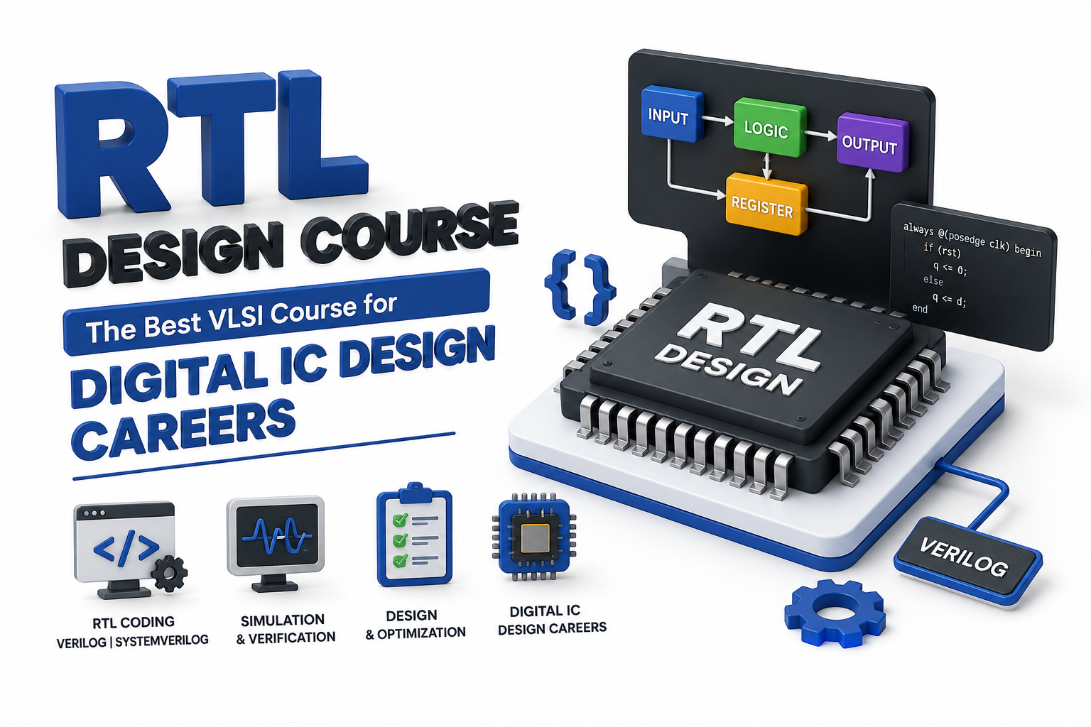
An RTL (Register Transfer Level) Design Course is widely regarded as one of the best VLSI courses for freshers and working professionals who want to build a career in digital IC design. RTL design forms the foundation of modern semiconductor chip development, where engineers describe digital hardware behavior using Hardware Description Languages (HDLs) such as Verilog and SystemVerilog. A comprehensive RTL Design course covers digital electronics fundamentals, combinational and sequential logic, finite state machines (FSMs), coding guidelines, synthesis concepts, timing constraints, and FPGA-based implementation. Through hands-on projects, learners gain practical experience in designing efficient, synthesizable, and scalable digital circuits that meet industry standards for ASIC and FPGA development.
With the rapid growth of AI processors, automotive electronics, IoT devices, 5G communication systems, and high-performance computing, the demand for skilled RTL Design Engineers continues to rise across India's semiconductor industry. Completing an industry-oriented RTL Design course equips learners with practical skills in RTL coding, simulation, debugging, linting, synthesis, and design optimization using leading EDA tools. These job-ready competencies open career opportunities in roles such as RTL Design Engineer, FPGA Design Engineer, Digital Design Engineer, ASIC Design Engineer, and SoC Design Engineer. For anyone looking to enter the semiconductor industry or advance their VLSI career, an RTL Design course offers a strong technical foundation and excellent long-term career growth.
ASIC Design and Verification Course – Build Expertise in Chip Design and Functional Verification
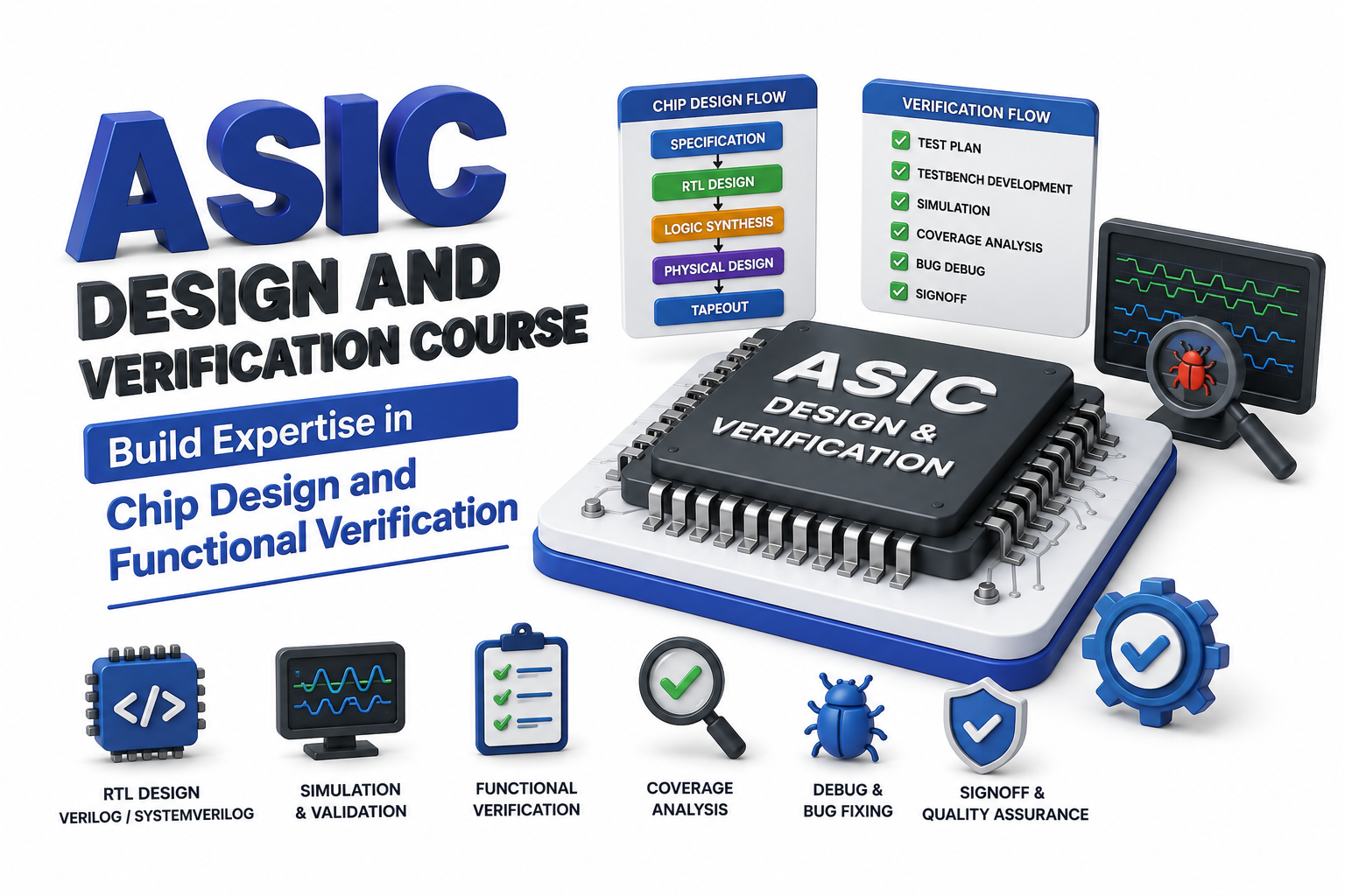
An ASIC (Application-Specific Integrated Circuit) Design and Verification Course is one of the most valuable VLSI training programs for freshers and working professionals aiming to build a career in semiconductor chip design. ASICs are custom-designed integrated circuits developed for specific applications such as artificial intelligence (AI), automotive electronics, consumer devices, networking equipment, healthcare systems, and data centers. A comprehensive ASIC Design and Verification course introduces learners to the complete ASIC design flow, including digital logic design, RTL coding using Verilog and SystemVerilog, synthesis, simulation, timing analysis, and design optimization. By understanding each stage of the chip development lifecycle, learners gain the technical knowledge required to contribute to complex semiconductor projects.
The functional verification segment of the course focuses on ensuring that an ASIC performs according to its design specifications before fabrication. Students learn advanced verification methodologies using SystemVerilog and Universal Verification Methodology (UVM), along with assertions, constrained-random testing, functional coverage, regression testing, and debugging techniques. Practical training on industry-standard EDA tools enables learners to create reusable verification environments, identify design bugs early, and improve overall chip quality. Since verification accounts for a significant portion of modern ASIC development, professionals with strong verification expertise are highly valued by semiconductor companies.
Completing an ASIC Design and Verification course prepares candidates for a wide range of career opportunities, including ASIC Design Engineer, ASIC Verification Engineer, RTL Design Engineer, SoC Verification Engineer, Digital Design Engineer, and Functional Verification Engineer. As India's semiconductor ecosystem continues to expand with increasing investments in chip design and manufacturing, the demand for engineers skilled in ASIC design, RTL development, and functional verification is growing rapidly. Choosing an industry-oriented ASIC Design and Verification course with real-world projects, hands-on tool experience, and placement support can significantly enhance your technical expertise and improve your chances of securing high-paying roles in leading semiconductor companies.
Physical Design Course – Learn Floorplanning, Placement, Clock Tree Synthesis, and Routing
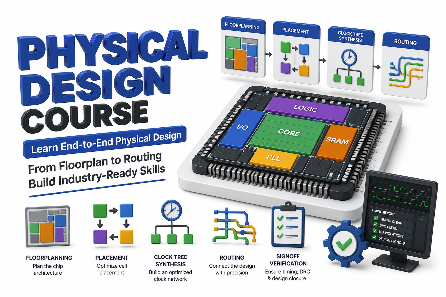
A Physical Design Course is one of the most sought-after VLSI courses for freshers and working professionals who want to specialize in the backend semiconductor design flow. Physical design is the process of converting a synthesized netlist into a manufacturable chip layout while ensuring optimal performance, power efficiency, and silicon area utilization. A comprehensive Physical Design course covers every stage of the ASIC implementation flow, including floorplanning, power planning, cell placement, Clock Tree Synthesis (CTS), routing, congestion analysis, parasitic extraction, and physical verification. Learners also gain practical exposure to industry-standard EDA tools, enabling them to understand how complex System-on-Chip (SoC) designs are transformed into fabrication-ready layouts.
With the rapid expansion of AI accelerators, 5G infrastructure, automotive electronics, and high-performance computing, skilled Physical Design Engineers are in high demand across India's semiconductor industry. An industry-focused Physical Design course equips learners with hands-on experience in timing closure, signal integrity analysis, IR drop optimization, electromigration checks, Design Rule Checking (DRC), Layout Versus Schematic (LVS), and chip signoff methodologies. These practical skills prepare candidates for rewarding roles such as Physical Design Engineer, ASIC Backend Engineer, P&R Engineer, Implementation Engineer, and SoC Physical Design Engineer. For professionals seeking a high-growth career in VLSI, mastering physical design provides excellent job opportunities, competitive salaries, and the chance to contribute to cutting-edge semiconductor innovations.
DFT (Design for Testability) Course – Master Scan, ATPG, and Semiconductor Testing Techniques
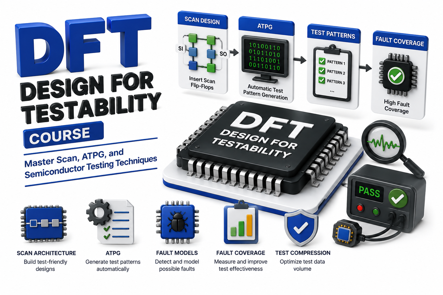
A DFT (Design for Testability) Course is an excellent choice for freshers and working professionals who want to build expertise in semiconductor testing and chip validation. Design for Testability is a critical stage of the ASIC design flow that ensures integrated circuits can be efficiently tested for manufacturing defects before they are delivered to customers. A comprehensive DFT course covers essential concepts such as scan chain insertion, scan compression, boundary scan (JTAG), Memory Built-In Self-Test (MBIST), Logic Built-In Self-Test (LBIST), Automatic Test Pattern Generation (ATPG), fault simulation, and test coverage analysis. Through hands-on training with industry-standard EDA tools, learners gain practical experience in implementing DFT architectures and improving the testability of complex digital designs.
As semiconductor devices become increasingly sophisticated, the demand for skilled DFT engineers continues to grow across industries including AI, automotive, consumer electronics, telecommunications, and high-performance computing. An industry-oriented DFT course equips learners with the knowledge to optimize fault coverage, reduce testing costs, enhance manufacturing yield, and ensure chip reliability without compromising design performance. These job-ready skills open career opportunities as DFT Engineer, ASIC Test Engineer, ATPG Engineer, Scan Design Engineer, and Semiconductor Validation Engineer. For anyone seeking a specialized and high-demand career in VLSI, mastering Design for Testability provides a strong competitive advantage and creates opportunities to work on advanced semiconductor technologies.
Static Timing Analysis (STA) Course – Gain In-Demand Timing Closure and Signoff Skills
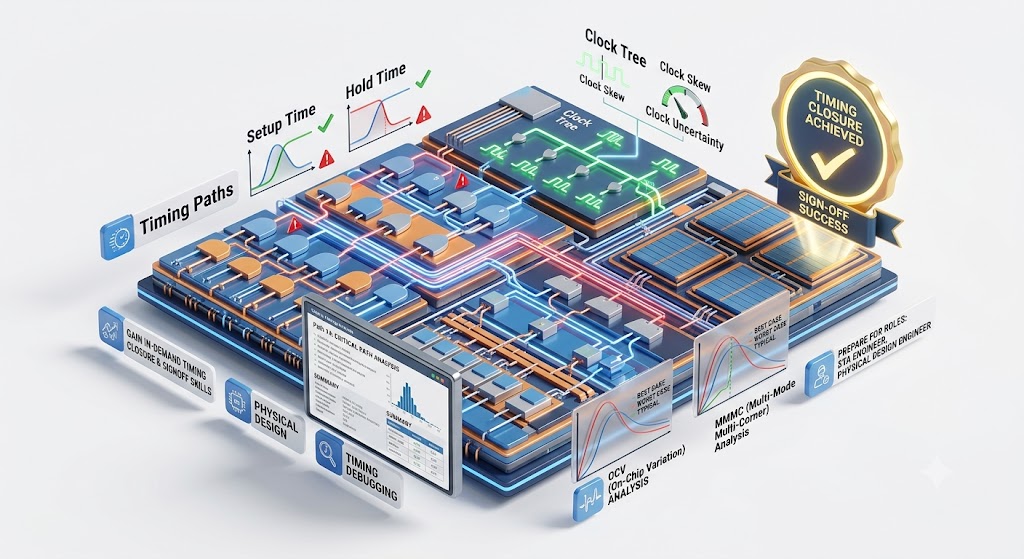
A Static Timing Analysis (STA) Course is one of the most valuable VLSI courses for engineers who want to specialize in ASIC physical design and chip signoff. Static Timing Analysis is a critical verification process used to ensure that a digital integrated circuit meets all timing requirements without relying on simulation. A comprehensive STA course covers essential concepts such as timing paths, setup and hold time analysis, clock skew, clock uncertainty, timing constraints (SDC), timing exceptions, multi-mode multi-corner (MMMC) analysis, on-chip variation (OCV), and timing optimization techniques. Learners also gain practical experience with industry-standard EDA tools to analyze timing reports, identify violations, and implement effective timing closure strategies for high-performance semiconductor designs.
As modern semiconductor chips become more complex and operate at higher frequencies, companies are actively seeking engineers with strong expertise in timing analysis and signoff methodologies. An industry-focused STA course equips learners with hands-on skills in timing debugging, constraint validation, ECO implementation, signoff verification, and performance optimization while ensuring low power consumption and design reliability. These specialized skills prepare candidates for roles such as STA Engineer, Physical Design Engineer, Timing Signoff Engineer, ASIC Backend Engineer, and SoC Implementation Engineer. For freshers and working professionals aiming to build a successful career in the semiconductor industry, mastering Static Timing Analysis significantly enhances employability and opens doors to high-paying opportunities in leading VLSI companies.
Analog IC Design Course – Learn Custom Circuit Design for High-Performance Semiconductor Chips
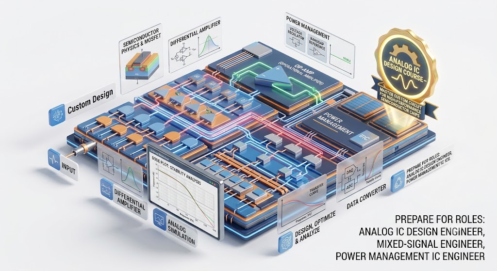
An Analog IC Design Course is an ideal choice for freshers and working professionals who aspire to build a career in custom integrated circuit design. Unlike digital circuits, analog circuits process continuous signals and are essential components in smartphones, medical devices, automotive electronics, IoT systems, communication equipment, and power management applications. A comprehensive Analog IC Design course covers semiconductor device physics, MOSFET operation, current mirrors, differential amplifiers, operational amplifiers (Op-Amps), bandgap references, voltage regulators, phase-locked loops (PLLs), data converters (ADC/DAC), and analog simulation techniques. Learners also gain hands-on experience with industry-standard EDA tools to design, simulate, analyze, and optimize high-performance analog circuits for real-world semiconductor applications.
With the rapid advancement of AI, 5G, electric vehicles, wearable devices, and high-speed communication technologies, the demand for skilled Analog IC Design Engineers continues to grow across the global semiconductor industry. An industry-oriented Analog IC Design course equips learners with practical skills in circuit analysis, transistor-level design, low-power optimization, noise analysis, stability evaluation, and performance verification. These in-demand competencies prepare candidates for rewarding roles such as Analog IC Design Engineer, Mixed-Signal Design Engineer, Custom Circuit Design Engineer, Power Management IC Engineer, and Semiconductor Design Engineer. For professionals seeking a specialized and high-growth career in VLSI, mastering Analog IC Design provides a strong technical foundation and excellent opportunities to work on next-generation semiconductor products.
Analog Layout Design Course – Develop Industry-Ready Skills in Custom Layout and Verification
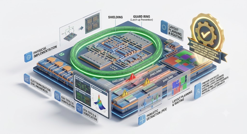
An Analog Layout Design Course is one of the best VLSI courses for freshers and working professionals who want to specialize in the physical implementation of analog and mixed-signal integrated circuits. Analog layout is a precision-driven process where the schematic design is converted into a manufacturable silicon layout while maintaining electrical performance, matching accuracy, and reliability. A comprehensive Analog Layout Design course covers transistor-level layout techniques, layout planning, device matching, common centroid layout, interdigitated structures, guard rings, shielding, routing strategies, parasitic extraction, and layout optimization. Learners also gain hands-on experience with industry-standard EDA tools to create high-quality layouts and perform physical verification using Design Rule Check (DRC), Layout Versus Schematic (LVS), and Parasitic Extraction (PEX).
As semiconductor technologies continue to advance in areas such as AI, automotive electronics, consumer devices, medical equipment, and wireless communication, the demand for skilled Analog Layout Engineers is steadily increasing. An industry-focused Analog Layout Design course equips learners with practical expertise in custom layout design, layout verification, electromigration awareness, latch-up prevention, and process-specific design techniques. These job-ready skills prepare candidates for career opportunities as Analog Layout Engineer, Custom Layout Engineer, Mixed-Signal Layout Engineer, Physical Layout Engineer, and Semiconductor Layout Design Engineer. By mastering analog layout methodologies and verification processes, professionals can contribute to the development of high-performance, low-power, and reliable semiconductor chips used in today's most advanced electronic systems.
Embedded Systems and FPGA Design Course – Bridge Hardware and Software Development
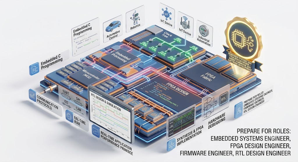
An Embedded Systems and FPGA Design Course is an excellent choice for freshers and working professionals who want to develop expertise in both hardware and software development. Embedded systems are the backbone of modern electronic products, powering applications such as automotive control units, industrial automation, robotics, consumer electronics, IoT devices, medical equipment, and communication systems. A comprehensive course covers embedded C programming, microcontrollers, processor architecture, peripherals, communication protocols such as UART, SPI, I2C, and CAN, along with FPGA design using Verilog or VHDL. Learners also gain practical experience in RTL design, simulation, synthesis, FPGA implementation, and hardware debugging using industry-standard development boards and EDA tools.
With the growing adoption of AI, edge computing, 5G networks, autonomous vehicles, and smart devices, professionals with expertise in embedded systems and FPGA design are in high demand across the semiconductor and electronics industries. An industry-oriented Embedded Systems and FPGA Design course equips learners with hands-on skills in hardware-software integration, digital system design, real-time application development, FPGA prototyping, and performance optimization. These industry-ready competencies prepare candidates for roles such as Embedded Systems Engineer, FPGA Design Engineer, Firmware Engineer, RTL Design Engineer, Hardware Design Engineer, and IoT Engineer. For individuals seeking a future-proof career in VLSI and embedded technology, mastering embedded systems and FPGA design provides a strong technical foundation and excellent opportunities in rapidly evolving technology sectors.
SoC Design and Verification Course – Learn Advanced System-on-Chip Architecture and UVM Methodologies
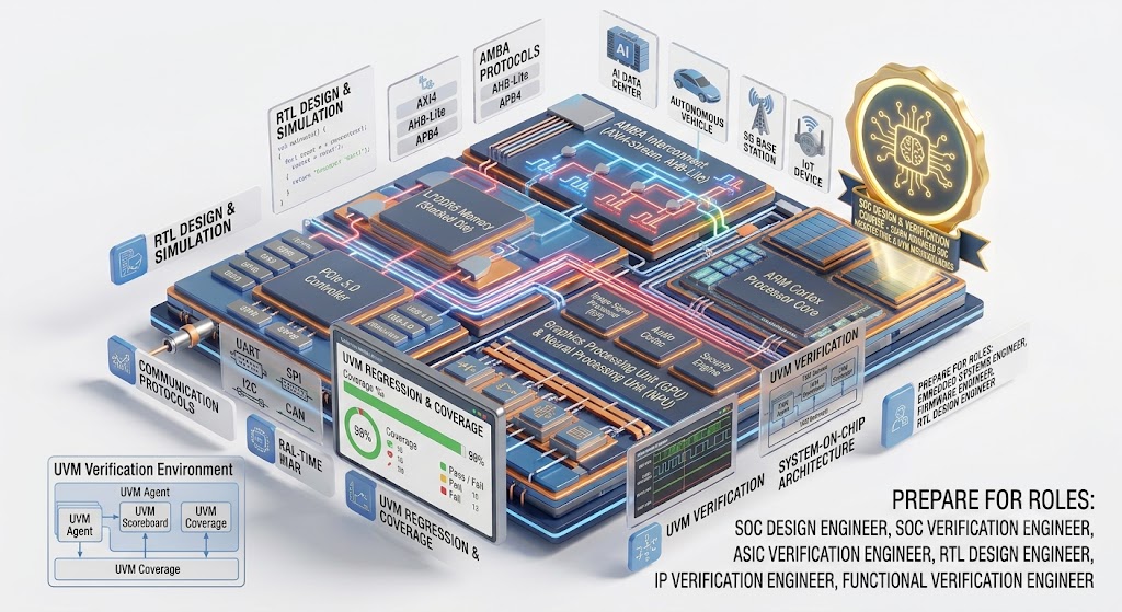
A System-on-Chip (SoC) Design and Verification Course is one of the most advanced VLSI courses for freshers and working professionals who want to build expertise in designing and verifying complex semiconductor chips. A System-on-Chip integrates multiple functional blocks, including processor cores, memory, communication interfaces, graphics units, and peripheral controllers, onto a single integrated circuit. A comprehensive SoC Design and Verification course covers SoC architecture, RTL design, AMBA protocols such as AXI, AHB, and APB, IP integration, clock and reset management, simulation, and functional verification using SystemVerilog and Universal Verification Methodology (UVM). Learners gain hands-on experience in developing scalable verification environments, writing reusable testbenches, creating constrained-random test cases, collecting functional coverage, and debugging complex SoC designs using industry-standard EDA tools.
As semiconductor companies continue to develop high-performance chips for artificial intelligence, automotive electronics, 5G communication, data centers, consumer electronics, and IoT applications, the demand for skilled SoC Design and Verification Engineers is growing rapidly. An industry-oriented SoC Design and Verification course equips learners with practical skills in IP verification, protocol verification, assertions, regression testing, coverage-driven verification, and chip-level validation. These in-demand competencies prepare candidates for rewarding roles such as SoC Design Engineer, SoC Verification Engineer, ASIC Verification Engineer, RTL Design Engineer, IP Verification Engineer, and Functional Verification Engineer. For professionals aiming to build a successful career in the semiconductor industry, mastering SoC architecture and UVM methodologies provides a competitive advantage and opens the door to opportunities in leading VLSI and chip design companies.
VLSI Course Selection Guide – How Freshers and Working Professionals Can Choose the Right VLSI Training Program
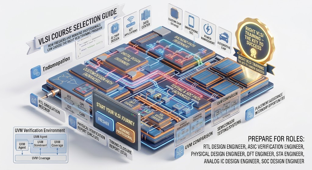
Choosing the right VLSI training program is one of the most important decisions for anyone planning to build a successful career in the semiconductor industry. With numerous VLSI courses available in India, freshers and working professionals should evaluate programs based on their career goals, educational background, and industry demand. Beginners interested in digital chip development can opt for RTL Design or ASIC Design courses, while those aiming for backend implementation may choose Physical Design or Static Timing Analysis (STA). Professionals looking to specialize in custom circuit development can consider Analog IC Design or Analog Layout Design, whereas candidates interested in semiconductor testing can pursue a DFT (Design for Testability) course. Selecting a course that offers an industry-relevant curriculum, hands-on projects, real-time EDA tool training, and experienced mentors significantly improves practical knowledge and job readiness.
Apart from the course syllabus, learners should also consider factors such as placement assistance, internship opportunities, certification, live project exposure, and the institute's industry reputation before enrolling in a VLSI training program. The best VLSI courses focus on practical implementation rather than theory alone, helping students gain expertise in industry-standard tools, design methodologies, debugging techniques, and semiconductor workflows. Whether you are a fresher starting your VLSI journey or a working professional planning a career transition, choosing the right training program can enhance your technical skills, improve your employability, and open doors to rewarding roles such as RTL Design Engineer, ASIC Verification Engineer, Physical Design Engineer, DFT Engineer, STA Engineer, Analog IC Design Engineer, and SoC Design Engineer in leading semiconductor companies.