

Top 59 Post-Silicon Validation Interview Questions and Answers (2026)
Navigate through this article using the table of contents below
Table of Contents
No headings found in this article.
Preparing for a post-silicon validation interview requires more than memorizing definitions—it demands a solid understanding of real-world chip debugging, hardware validation, performance analysis, and problem-solving. Top semiconductor companies expect candidates to demonstrate practical knowledge of silicon bring-up, protocol validation, power optimization, and reliability testing while working with complex hardware platforms.
Whether you are a recent graduate, an ECE student, or an experienced engineer looking to advance your career, this collection of interview questions and answers is designed to help you build confidence and strengthen your technical foundation. If you're also enrolled in a post silicon validation course, these questions can serve as an excellent resource to reinforce your learning and prepare for technical interviews.
In this guide, you'll find 59 carefully selected post-silicon validation interview questions covering fundamentals, debugging scenarios, tools and infrastructure, power and thermal concepts, protocol and interface validation, and career-focused topics. Each answer is written with an industry-oriented approach to help you understand not just the theory but also the practical thinking expected by leading semiconductor companies.
[01] Interview Question Based on Fundamentals & Core Concepts

Tests your foundational understanding of post-silicon validation — what every interviewer asks first.
Q1. What is post-silicon validation and how does it differ from pre-silicon verification?
Answer: Post-silicon validation is the process of testing and validating an actual fabricated silicon chip to confirm it matches its RTL design intent and meets functional, performance, and power specifications. Pre-silicon verification is simulation-based — it runs on RTL models using tools like Synopsys VCS or Cadence Xcelium and can achieve 100% controllability and observability. Post-silicon works on real hardware at real speed, which means limited internal signal visibility, real-world noise, process variation effects, and no ability to pause-and-inspect. The two are complementary: pre-silicon catches most logical bugs; post-silicon catches timing violations, electromigration issues, power-grid noise, and silicon-specific failures that simulation cannot model faithfully.
Q2. What are the key phases in a typical post-silicon validation flow?
Answer: A complete post-silicon validation flow typically spans: (1) Bring-up — powering the chip for the first time, establishing basic clock and I/O functionality; (2) Functional Validation — running directed and pseudo-random tests to confirm functional correctness; (3) Performance Characterization — measuring frequency, throughput, and latency against spec; (4) Power Measurement — validating static leakage, dynamic power, and thermal behavior; (5) Debug and Root-Cause Analysis — isolating and identifying silicon bugs using logic analyzers, oscilloscopes, and scan-based techniques; (6) Silicon Sign-off — generating a test coverage report and releasing to production.
Q3. What is the role of scan chains in post-silicon validation?
Answer: Scan chains are DFT (Design for Test) structures where flip-flops in a design are connected into a shift register. In post-silicon validation, scan chains allow engineers to load specific state into the chip's registers (scan-in) and read back the resulting state (scan-out) without requiring direct probe access to internal nodes. This enables controllability and observability on silicon — critical when debugging a hardware failure that simulation cannot replicate. Engineers use JTAG (IEEE 1149.1) as the standard interface to access scan chains on physical silicon.
Q4. What is JTAG and why is it important in post-silicon debug?
Answer: JTAG (Joint Test Action Group, IEEE 1149.1) is a standardized serial interface that provides access to a chip's test logic via four signals: TDI, TDO, TMS, and TCK. In post-silicon validation, JTAG enables: reading and writing chip registers, loading scan chains, accessing embedded trace buffers, programming on-chip memories, and controlling reset/clock sequences. Modern SoCs extend JTAG with Coresight (ARM) or custom debug subsystems to expose additional debug primitives. Without JTAG access, debugging a silent silicon failure on a complex SoC would be extremely difficult.
Q5. Explain what 'silicon bring-up' means and list the typical steps involved.
Answer: Silicon bring-up is the first contact with a newly fabricated chip — the process of getting it to power up, respond to clocks, and execute its first instruction or transaction. Typical steps: (1) Power sequence validation — confirm all voltage rails come up in the correct order and within tolerance; (2) Clock validation — verify PLLs lock and output clocks are at correct frequencies; (3) Reset release — confirm chip exits reset cleanly; (4) JTAG/debug port connectivity — establish a debug connection and confirm ID register reads correctly; (5) Basic read/write tests on internal registers; (6) First boot sequence — loading and executing a minimal firmware image. Failures at any step point to power, clock, or I/O interface issues.
Q6. What is the difference between a functional bug and a timing bug in silicon?
Answer: A functional bug means the chip produces logically incorrect output regardless of operating frequency — it is a design error in the RTL or in layout that alters logical behavior. A timing bug means the chip works correctly at lower frequencies but fails above a certain speed threshold — it is a timing violation where a signal does not meet setup or hold requirements. Timing bugs are silicon-specific: they result from process variation, wire delays, IR drop, or cell characterization inaccuracies that the pre-silicon STA (Static Timing Analysis) did not fully capture. Distinguishing the two during debug saves significant time — frequency sweep testing is the first step.
Q7. What are process corners and why do they matter in post-silicon validation?
Answer: Process corners represent the statistical spread in transistor and wire characteristics due to manufacturing variation. The standard corners are: TT (typical-typical), FF (fast-fast), SS (slow-slow), FS (fast NMOS, slow PMOS), and SF (slow NMOS, fast PMOS). In pre-silicon STA, all corners are simulated. In post-silicon, each fabricated die lands at some point in this distribution — and validation engineers must test across temperature and voltage to ensure the chip functions across its full operating envelope, not just at nominal conditions. Lot sampling at different process corners is standard qualification practice.
Q8. What is an Automated Test Equipment (ATE) and how is it used in post-silicon validation?
Answer: ATE is specialized hardware used in production testing of semiconductor devices. In post-silicon validation, ATE platforms like Advantest V93000 or Teradyne UltraFLEX are used to apply stimulus vectors, measure responses, and characterize parametric performance at speed. ATE enables high-volume testing under controlled conditions — applying ATPG (Automatic Test Pattern Generation) patterns for stuck-at fault coverage, measuring leakage and IDDQ current, and performing speed binning. The validation team works closely with ATE teams to translate lab findings into ATE test patterns that can run in production.
Q9. What is IR drop and what are its implications in post-silicon validation?
Answer: IR drop is the voltage drop across the power delivery network (PDN) of a chip — caused by the resistance (R) of metal interconnects when current (I) flows through them. Significant IR drop at active regions means those transistors see lower-than-nominal supply voltage, reducing their switching speed and potentially causing timing violations or functional failures. In post-silicon validation, dynamic IR drop events (caused by simultaneous switching of large logic blocks) are identified by measuring supply voltage with a high-bandwidth oscilloscope at the power pins and correlating drops with test patterns. Decoupling capacitor placement and power grid analysis are used to mitigate it.
Q10. What is electromigration and how does it affect silicon reliability validation?
Answer: Electromigration (EM) is the gradual physical displacement of metal atoms in interconnects under sustained high current density, eventually causing open circuits or short circuits. It is a reliability mechanism, not an immediate functional failure — EM-induced failures can take months or years to manifest under normal operating conditions. In post-silicon validation, EM is addressed through accelerated life testing (ALT) at elevated temperature and current, using Black's equation to extrapolate mean time to failure (MTTF) at operating conditions. Validation engineers confirm that all power and signal routes meet EM design rules from the PDK before silicon sign-off.
[02] Interview Question Based On Scenario-Based & Debug Questions
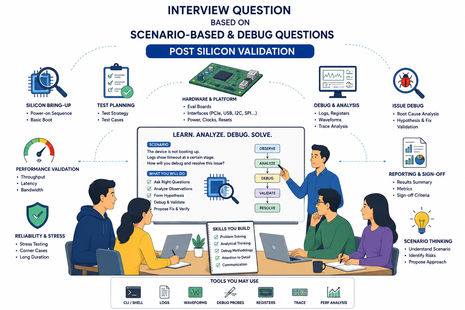
Real silicon debugging scenarios — the category that separates prepared engineers from the rest.
Q11. Your chip passes all pre-silicon simulations but fails on first power-up. Walk through your debug approach.
Answer: Start with the power delivery network — confirm all voltage rails are at correct levels and in correct sequence using a multimeter and oscilloscope. Next, check clock outputs: are PLLs locked? Is the reference clock reaching the chip? Then attempt JTAG connectivity — if JTAG does not respond, the chip may be in a bad reset state or there is a PCB routing issue. Check the board schematic for pull-up/pull-down errors on reset and boot configuration pins. If JTAG connects, read the chip ID register to confirm basic functionality. Then scan-in a known state and scan-out to isolate whether the issue is clocking, reset logic, or a deeper functional block. Document every reading — the pattern of failures often points to the root cause faster than any single test.
Q12. You observe that a chip passes at 25°C but fails intermittently at 85°C. What is your methodology?
Answer: This is a classic thermal/timing margin issue. First, confirm it is reproducible and note the exact fail pattern — which tests fail, at what frequency. Then perform a voltage-temperature (VT) corner sweep: test at multiple voltage points (nominal, 5% below nominal) across 25°C, 55°C, 85°C, 105°C. If failures increase at high temperature and low voltage, this strongly indicates a setup timing violation — transistors are slower at high temperature and low voltage. Use a logic analyzer or on-chip timing monitors (if available) to identify the failing path. Cross-reference with pre-silicon STA reports to find paths with the tightest timing margin at the worst-case corner. Feed the finding back to the timing team for ECO (Engineering Change Order) or clock frequency guard-banding.
Q13. A silicon bug is found that did not appear in pre-silicon simulation. How do you determine whether it is a DV miss or a silicon-unique issue?
Answer: Start by reproducing the failure on silicon with a minimal, deterministic test sequence — reduce the test to the fewest steps that still trigger the bug. Then attempt to reproduce the exact same sequence in RTL simulation. If simulation reproduces the failure, it is a DV miss — the testbench did not cover this corner case. If simulation does not reproduce it with identical inputs, it is likely silicon-unique: candidates include a timing violation (add clock uncertainty and model real delays in simulation), a power supply noise event (check dynamic IR drop at the failing moment), a process-corner sensitivity (re-run sim at SS/worst-case corner), or an analog/mixed-signal interface issue. Document the reproduction steps rigorously — this becomes the regression test after the fix.
Q14. How would you debug a PCIe link that fails to train to Gen3 speed on silicon but works at Gen1?
Answer: PCIe link training failure at Gen3 while passing Gen1 is almost always a signal integrity issue — the higher frequency reveals marginal I/O performance. Debug steps: (1) Use a protocol analyzer (e.g., LeCroy PCIe analyzer) to capture the LTSSM (Link Training and Status State Machine) logs and identify at which state the training stalls; (2) Measure eye diagrams on the Tx lanes using a high-bandwidth oscilloscope — check eye height, eye width, and jitter against PCIe Gen3 spec (8 GT/s); (3) Check Rx equalization settings — Gen3 requires active equalization, confirm the preset/preset values are optimal; (4) Inspect PCB trace length matching and via placement for return loss and insertion loss; (5) Check if reducing the operating voltage or temperature makes it worse, pointing to a specific margin issue. Feed eye diagram data back to the physical design team for analysis.
Q15. Your test shows IDDQ (quiescent current) is 3x higher than expected. What are the possible causes and how do you isolate?
Answer: Elevated IDDQ indicates excess leakage current when the chip is in a static state. Possible causes: (1) Excessive gate leakage due to thin-oxide cells — check if the design uses appropriate multi-Vt cells; (2) Short-circuit path in the power grid — possibly a metal bridge introduced during layout; (3) Latch-up — an SCR-like parasitic structure is conducting, common if ESD events occurred during handling; (4) Hot carrier injection damage from prior overvoltage testing; (5) Normal process variation at a fast corner. Isolation approach: use power domain isolation (if available) to selectively power blocks and measure IDDQ per domain to localize the offending block. Cross-section SEM analysis can identify physical shorts in suspect areas.
Q16. Describe how you would use an on-chip logic analyzer (e.g., Synopsys Identify or Xilinx ILA) during post-silicon debug.
Answer: On-chip logic analyzers (OLAs) are pre-inserted debug RTL that sample internal signals into on-chip SRAM at full operating frequency — solving the internal observability problem. To use one: (1) Define trigger conditions — specify which signal state or event should start capture; (2) Select signals to capture — typically the signals around the suspected failing block; (3) Configure capture depth and pre-trigger samples; (4) Run the failing test and wait for the trigger to fire; (5) Read back captured data via JTAG or debug bus and display as a waveform in the companion software. OLAs are invaluable for catching single-cycle glitches or handshake protocol violations that are invisible to external probing. Their limitation is that they must be pre-planned before tape-out — you cannot add signals after silicon is back.
Q17. A DDR5 memory controller on your chip fails ECC tests only when the memory is accessed in burst mode. How do you approach this?
Answer: ECC failure only in burst mode suggests a timing or data integrity issue specific to high-bandwidth access patterns. Approach: (1) Capture the DDR5 bus transactions using a memory bus analyzer — look for out-of-spec signal levels, setup/hold violations, or data eye closure on DQ/DQS; (2) Check the read/write leveling calibration — burst mode stresses the DQS-DQ alignment more than single transfers; (3) Isolate whether the ECC error is consistent (same bit position) or random (multiple positions). Consistent errors point to a failing data path lane; random errors point to a marginal timing window; (4) Run a memory stress test (e.g., PRBS pattern) at reduced frequency to find the frequency at which it starts to pass — this bounds the timing margin; (5) Compare DQ eye diagrams at burst vs. non-burst to confirm eye closure.
Q18. How do you handle a silicon bug found in production silicon where a re-spin is not feasible?
Answer: When a re-spin is not an option, the path forward is a software or firmware workaround. Steps: (1) Precisely characterize the bug — under exactly what conditions does it trigger? What is the minimum reproducible case? (2) Determine if the failure mode is avoidable by changing usage patterns — for example, disabling a specific power state, limiting clock frequency, or flushing a cache at specific intervals; (3) Work with the firmware/driver team to implement the workaround at the lowest possible software layer; (4) Validate the workaround on silicon across all temperature and voltage corners; (5) Document the errata clearly with the trigger condition, impact, and workaround — this becomes a customer-facing errata document; (6) Feed the root cause back to RTL and DV teams to ensure the next revision has both the fix and a regression test.
Q19. What is a silicon stepping and why is it done?
Answer: A silicon stepping (also called an ECO spin or metal spin) is a targeted revision to an existing chip design to fix a known set of bugs without redesigning the entire chip from scratch. Unlike a full re-spin, a metal ECO only changes the metal routing layers — adding or removing connections between cells that are already placed — which is significantly cheaper and faster (weeks instead of months). Steppings are done when: (1) A critical functional bug is found post-production; (2) A timing violation needs a targeted fix; (3) A power consumption issue requires gate substitution. Validation engineers are responsible for creating a regression test suite that specifically validates each ECO fix on the new stepping before it is approved for production.
Q20. During bring-up, your chip's PLL fails to lock. List your systematic debug steps.
Answer: PLL lock failure is one of the most common bring-up issues. Systematic debug: (1) Confirm reference clock — measure the input reference at the chip pin with an oscilloscope. Verify frequency, amplitude, duty cycle, and jitter all meet the PLL's input spec; (2) Check power supply to the PLL — analog PLLs often have a separate, filtered supply (AVDD). Confirm it is clean and at the correct level; (3) Verify PLL bypass mode — if the chip supports it, put the PLL in bypass and use the reference clock directly to determine if the rest of the chip functions, isolating the PLL itself; (4) Check configuration registers — confirm the PLL's M, N, and divider settings are correctly programmed via JTAG or I2C; (5) Inspect the loop filter capacitors on the PCB — missing or wrong-value loop filter components will prevent lock; (6) Test across temperature — some PLLs have a narrow VCO tuning range that fails at cold corners.
[03] Interview Question Based On Tools & Infrastructure Questions

Know your instruments — validation roles demand hands-on tool proficiency from day one.
Q21. What instruments are commonly used in a post-silicon validation lab and what is each used for?
Answer: Key lab instruments: (1) Oscilloscope (high-bandwidth, 20GHz+) — for measuring signal integrity, clock jitter, power supply ripple, and eye diagrams; (2) Logic Analyzer — for capturing multi-signal digital bus transactions and correlating events; (3) Protocol Analyzer (PCIe, USB, DDR, Ethernet) — for decoding and verifying high-speed protocol traffic; (4) Power Analyzer (e.g., Yokogawa WT series) — for measuring dynamic power consumption and efficiency; (5) JTAG Debugger (e.g., Lauterbach Trace32, ARM DS-5) — for register access and scan-chain debug; (6) Thermal Camera — for identifying hot spots caused by excessive power dissipation; (7) ATE (Advantest, Teradyne) — for structured test pattern execution and parametric measurement at volume.
Q22. What is Lauterbach Trace32 and how is it used in post-silicon validation?
Answer: Lauterbach Trace32 is the industry's most widely used hardware debugger for embedded systems and SoC post-silicon debug. It connects to the chip via JTAG or SWD (Serial Wire Debug) and provides: register-level read/write access, memory dump and modification, real-time trace (via ETM/PTM trace ports), breakpoint setting, and disassembly of executing code. In post-silicon validation, Trace32 is typically the first tool connected during bring-up. It allows validation engineers to read chip ID registers, load firmware, single-step through boot code, and halt the processor at a specific address to inspect state — all without physical probing of internal nodes.
Q23. Explain how eye diagram measurements work and what parameters you analyze.
Answer: An eye diagram is generated by overlaying millions of consecutive bit transitions from a high-speed serial signal on top of each other, creating a composite waveform that resembles an open eye. It is captured using an oscilloscope in persistence mode or with a sampling oscilloscope. Key parameters: (1) Eye Height — vertical opening, must exceed the receiver's minimum differential input voltage; (2) Eye Width — horizontal opening, must exceed the receiver's required data valid window; (3) Eye Crossing Percentage — where clock edges land, should be near 50% for symmetric crossings; (4) RMS Jitter and Deterministic Jitter — jitter degrades eye width; (5) Q-factor / BER estimate — statistical measure of eye quality. These parameters are measured against the relevant specification (PCIe, USB, DDR, Ethernet) to confirm signal integrity compliance.
Q24. What is BERT (Bit Error Rate Tester) and how is it used in high-speed interface validation?
Answer: A BERT is an instrument that generates a known data pattern (PRBS — Pseudo-Random Bit Sequence, typically PRBS7, PRBS15, PRBS31) and transmits it through a high-speed serial link, then receives the signal and compares it against the expected pattern to count errors. In post-silicon validation of PCIe, USB, Ethernet, or SATA interfaces: (1) BERT generates stress patterns that exercise the worst-case transitions; (2) The link under test attempts to receive and decode them; (3) Bit Error Rate (BER) is measured — production specs typically require BER < 10^-12; (4) BER is measured as a function of frequency, voltage, and temperature to find the operating margin. BERT testing is essential for PHY-level sign-off.
Q25. How do you use Python scripting in a post-silicon validation environment?
Answer: Python is the dominant scripting language in modern validation labs. Common uses: (1) Test automation — writing test scripts that send commands to instruments via GPIB/USB/LAN using PyVISA or vendor-specific libraries, then parse and log results; (2) Data analysis — processing large CSV or binary log files from oscilloscopes or ATE using Pandas and NumPy to extract statistics, plot eye diagrams, or generate pass/fail summaries; (3) Register access — scripting JTAG read/write sequences via vendor APIs (e.g., OpenOCD, Trace32 PRACTICE API); (4) Regression management — scheduling and tracking test runs, collecting results, and flagging regressions; (5) Silicon characterization — sweeping voltage/frequency/temperature and plotting frequency vs. voltage curves (Fmax characterization).
Q26. What is JTAG TAP (Test Access Port) and how does a TAP controller state machine work?
Answer: The TAP is the hardware interface defined by IEEE 1149.1 JTAG. It has four mandatory pins: TDI (data in), TDO (data out), TMS (mode select), TCK (clock). The TAP Controller is a 16-state Moore state machine driven by TMS. Key states include: Test-Logic-Reset, Run-Test/Idle, Shift-DR, Shift-IR, Capture-DR, Update-DR. To access a register: (1) Navigate to Shift-IR state, shift in the register's instruction code; (2) Navigate to Shift-DR state, shift data in via TDI, data shifts out via TDO simultaneously; (3) Navigate to Update-DR to latch the new value. Understanding the TAP state machine is essential when manually constructing JTAG sequences for custom debug scenarios or when debugging JTAG access failures during bring-up.
Q27. What is an Embedded Trace Buffer (ETB) and how is it used for post-silicon debug?
Answer: An Embedded Trace Buffer is an on-chip SRAM that stores trace data generated by a processor's Embedded Trace Macrocell (ETM). The ETM continuously records executed instructions (instruction trace) or data accesses (data trace) in a compressed format. The ETB stores the last N cycles of trace before a trigger event, enabling post-mortem analysis. In post-silicon validation: (1) Configure the ETM to trace a specific address range; (2) Run the failing test; (3) Trigger the ETB capture on the failure event; (4) Retrieve trace data via JTAG and decode in Lauterbach Trace32 or ARM DS-5; (5) Reconstruct the exact execution path leading to the failure. This is particularly valuable for debugging boot failures or OS crashes where the failure event is transient.
Q28. What is STDF (Standard Test Data Format) and why is it important in silicon validation?
Answer: STDF is the industry-standard binary file format (JEDEC standard) used by ATE systems to store test results, including pass/fail outcomes, parametric measurements, and test conditions for each device under test. Every major ATE platform (Advantest, Teradyne) outputs STDF files. In post-silicon validation and production testing, STDF enables: (1) Wafer map generation — plotting pass/fail across the wafer to identify systematic yield issues; (2) Parametric trending — monitoring test limits over multiple lots for process drift; (3) Failure analysis input — directing which dice to pull for physical failure analysis; (4) Cross-site correlation — comparing ATE results between different test sites. Tools like Synopsys Galaxy Yield Management or Python-based STDF parsers (Semi-ATE) process STDF data for analysis.
Q29. What is voltage margining and how is it performed on silicon?
Answer: Voltage margining is the process of systematically varying the supply voltage above and below nominal while running functional tests to characterize the voltage operating margin of a chip. It reveals how much voltage headroom exists before failures occur, confirming that the chip has adequate margin against power supply variation in system deployment. Method: (1) Set up a programmable power supply with fine voltage control (1-5mV steps); (2) Run a functional test suite at each voltage point across the full temperature range; (3) Record the minimum voltage at which all tests pass (Vmin) and the maximum voltage before failures or latch-up (Vmax); (4) Compare Vmin/Vmax against the product specification; (5) Cross-correlate with IR drop simulations to confirm the Vmin is consistent with worst-case IR drop predictions.
Q30. What is the difference between stuck-at fault testing and transition fault testing?
Answer: Stuck-at fault (SAF) testing checks for nodes that are permanently stuck at logic 0 or logic 1 — the classical manufacturing defect model. ATPG generates patterns to detect each possible stuck-at fault across all nodes. Transition fault (TF) testing checks whether a node can make a 0→1 or 1→0 transition within the required time window — it detects delay defects like resistive opens or shorts that slow transitions without making them permanently stuck. TF coverage is essential for modern deep-submicron processes where resistive defects are common. In post-silicon validation, both SAF and TF patterns are applied via ATE. High SAF coverage (>99%) and high TF coverage (>95%) are typically required for production sign-off. TF patterns require at-speed testing on ATE, which adds infrastructure requirements.
[04] Interview Question Based On Power, Thermal & Reliability Questions
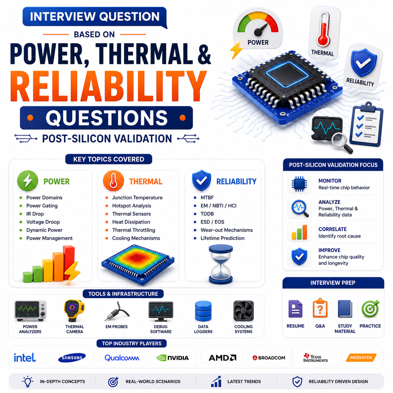
Critical for automotive, mobile, and AI chip roles — power validation is increasingly a standalone discipline.
Q31. What are the key metrics measured during power validation of a silicon chip?
Answer: Power validation measures: (1) Static/Standby Leakage (IDDQ) — current drawn when the chip is in a powered-but-idle state; (2) Dynamic Power — power consumed during active switching, measured under representative workloads; (3) Peak Power — maximum instantaneous power draw, critical for package and board decoupling design; (4) Power State Transitions — confirming that low-power states (sleep, hibernate, retention) enter and exit correctly with correct current levels; (5) Thermal Resistance (theta_JA, theta_JC) — measuring junction-to-ambient and junction-to-case thermal resistance to validate thermal model accuracy; (6) Power Efficiency — performance per watt under various workloads, increasingly important for AI and mobile chip sign-off.
Q32. How do you measure dynamic power consumption on a physical chip?
Answer: Dynamic power measurement requires capturing current draw under real workload conditions. Method: (1) Insert a precision shunt resistor (1-10 milliohm) in series with the supply rail under measurement; (2) Use a high-bandwidth differential probe on the shunt to measure the voltage drop — calculate current as I = V/R; (3) Use a dedicated power analyzer (Yokogawa WT1800, Keysight N6705) for accurate power calculations including real and reactive components; (4) Run representative workloads — synthetic (e.g., CoreMark, SPEC CPU) and application-level (e.g., AI inference, video encoding); (5) Cross-correlate measured power with pre-silicon power estimates from Synopsys PrimeTime PX or Cadence Voltus. Discrepancies >20% warrant investigation into toggle rate assumptions in the simulation.
Q33. What is thermal runaway and how do post-silicon engineers guard against it during validation?
Answer: Thermal runaway occurs when increased temperature increases leakage current, which increases power dissipation, which further increases temperature — a positive feedback loop that can permanently damage silicon if unchecked. In CMOS, leakage current approximately doubles for every 10°C rise in temperature. Guard against it during validation by: (1) Always monitoring junction temperature (TJ) using on-chip digital temperature sensors (DTS) or thermal cameras during power-intensive tests; (2) Implementing software thermal shutdown (TJ > threshold) before running high-power tests; (3) Performing initial power tests at room temperature before thermal stress; (4) Using forced-air or liquid cooling rigs in the validation lab for high-TDP chips; (5) Validating all DVFS (Dynamic Voltage and Frequency Scaling) transitions to confirm the thermal management algorithm responds correctly.
Q34. What is DVFS and how do you validate it on silicon?
Answer: DVFS (Dynamic Voltage and Frequency Scaling) is a power management technique where the chip dynamically reduces both voltage and frequency during low-workload periods to save power, and increases them during high-demand periods. Validating DVFS on silicon: (1) Confirm all operating points (voltage-frequency pairs) are stable — run a stress test at each OPP (Operating Performance Point) for 30+ minutes; (2) Validate the transition itself — confirm the chip does not crash or corrupt state during a V/F transition by running a functional test that spans a transition; (3) Measure transition latency — confirm the chip meets its specified ramp-up time from lowest to highest OPP; (4) Test transition under thermal load — the DVFS governor must correctly throttle frequency when TJ approaches the thermal limit; (5) Validate retention states — confirm register/cache state is preserved when transitioning through power-gated states.
Q35. What is HTOL (High Temperature Operating Life) testing and what does it validate?
Answer: HTOL is an accelerated reliability test that stresses chips at elevated temperature (typically 125°C or 150°C) and nominal-to-maximum voltage while running continuous functional patterns, over a period of 1000+ hours. It is designed to accelerate time-dependent dielectric breakdown (TDDB), hot carrier injection (HCI), and negative bias temperature instability (NBTI) — failure mechanisms that degrade transistor characteristics over time. HTOL validates that a chip will meet its rated lifetime (typically 10 years at operating conditions) by running in accelerated conditions and applying Arrhenius-based acceleration factors to extrapolate to field conditions. Validation engineers work with reliability teams to define HTOL test vectors that exercise all critical circuit blocks and compare pre/post-HTOL parametric measurements to detect degradation.
Q36. What is negative bias temperature instability (NBTI) and why does it concern post-silicon validation engineers?
Answer: NBTI is a reliability degradation mechanism that affects PMOS transistors under negative gate bias at elevated temperature. Over time, interface traps form at the Si-SiO2 interface, causing the threshold voltage (Vth) of the PMOS to increase — the transistor becomes slower. This is a time-dependent effect: a chip that meets timing today may fail timing after 3-5 years of operation. Post-silicon validation engineers address NBTI by: (1) Measuring Vth shifts after accelerated NBTI stress (high temperature + negative Vgs on PMOS); (2) Running timing tests before and after NBTI stress to quantify performance degradation; (3) Confirming that the design team has incorporated NBTI margin in STA (typically 10-15% Vth shift guardbanding); (4) Validating AC recovery — NBTI partially recovers when gate bias is removed, so duty cycle of operation matters.
Q37. How do you validate power domain isolation cells during post-silicon bring-up?
Answer: Power domain isolation cells prevent signals from a powered-down domain from corrupting a still-active domain. Validation steps: (1) Power down the target domain while keeping the receiving domain active; (2) Confirm that all isolation cells correctly clamp their outputs to a defined logic level (typically 0 or 1 as designed); (3) Verify no X-propagation or glitch occurs on the isolation cell outputs during the power-down transition; (4) Check that the isolation enable signal is asserted before the supply falls and released only after the supply is stable — sequence violation is a common bug; (5) Read power status registers via JTAG to confirm the power management controller reports the correct state; (6) Test restore — power the domain back up and confirm the isolated signals correctly transition back to functional levels without glitch.
Q38. What is ESD (Electrostatic Discharge) testing in the context of silicon validation?
Answer: ESD testing confirms that a chip's ESD protection structures (diodes, clamps) protect the core circuits from electrostatic discharge events that occur during handling, assembly, and in the field. Standard test models: (1) HBM (Human Body Model) — simulates discharge from a person, 100pF capacitor discharged through 1.5kΩ, typically must survive ±2kV; (2) CDM (Charged Device Model) — simulates a chip picking up charge and discharging to ground, the most damaging model for modern chips; (3) MM (Machine Model) — simulates automated equipment discharge. Post-silicon validation engineers perform ESD qualification using TLP (Transmission Line Pulse) testing for characterization and HBM/CDM test systems for qualification. ESD test failures result in pin-level physical damage visible under optical microscope.
Q39. What is latch-up and how is it tested in silicon validation?
Answer: Latch-up is a condition where a parasitic PNPN silicon-controlled rectifier (SCR) structure in CMOS, formed between NWELL and PWELL, is triggered and creates a low-impedance path between VDD and VSS — effectively a near-short-circuit that draws massive current and can permanently destroy the chip. It is triggered by overvoltage transients, ESD events, or injection currents. Latch-up testing per JEDEC standard JESD78: (1) Apply supply overvoltage pulses at each I/O pin; (2) Force current injection (both positive and negative) into each I/O; (3) Monitor supply current — a latch-up event causes current to spike to the supply limit; (4) Power cycle and test functionality after each event. Passing latch-up requires that supply current returns to normal after the trigger is removed and the chip remains functional.
Q40. Explain soft errors and how radiation hardness is validated in silicon.
Answer: Soft errors (also called single-event upsets, SEUs) are transient bit flips in memory cells or flip-flops caused by energetic particles (cosmic rays, alpha particles from package materials) ionizing silicon and depositing charge that flips the stored logic state. Unlike hard errors, soft errors do not cause permanent damage — but they corrupt data and can crash systems. For space, automotive, and server chips, radiation hardness is validated through: (1) Alpha particle exposure testing using americium-241 sources; (2) Neutron beam testing at accelerator facilities; (3) Heavy ion testing for space qualification; (4) Statistical measurement of Soft Error Rate (SER) in FIT (Failures In Time) per Gbit of SRAM. Mitigation techniques validated on silicon include ECC on memories, SEDT-hardened flip-flops, and triple modular redundancy (TMR).
[05] Interview Question Based On Protocol & Interface Validation Questions
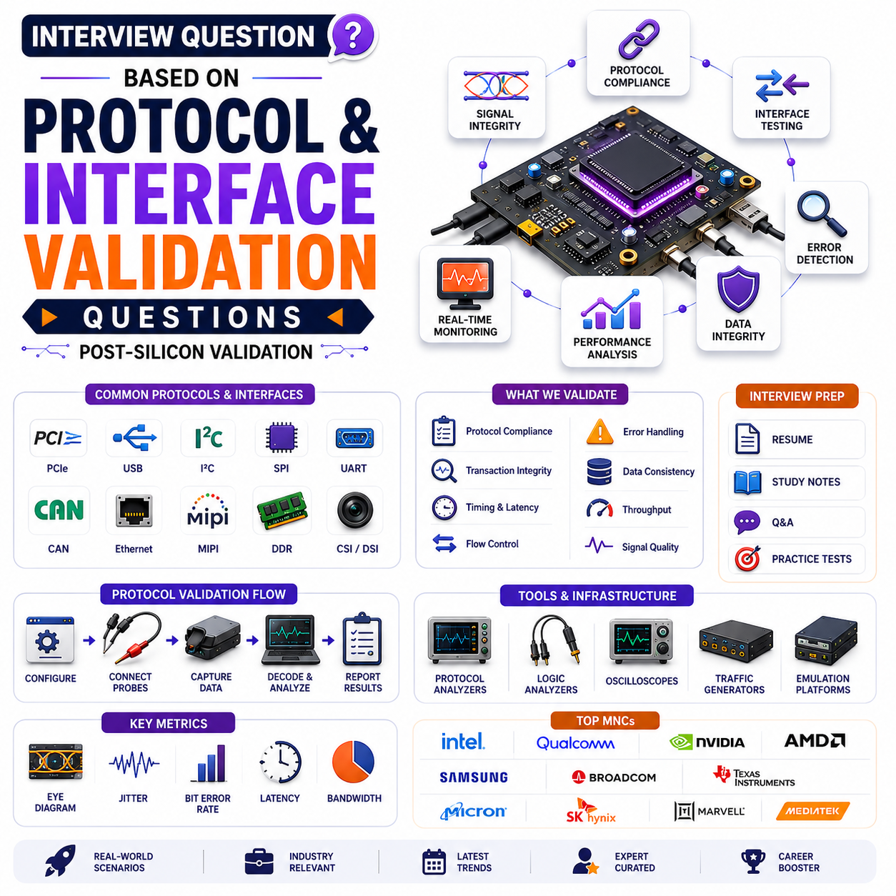
SoCs live and die by their interfaces — PCIe, DDR, USB, Ethernet, I2C/SPI are must-know territory.
Q41. Walk through the complete PCIe link training sequence and what can go wrong at each stage.
Answer: PCIe link training is managed by the LTSSM (Link Training and Status State Machine). Stages: (1) Detect — both TX and RX detect an impedance load on the lane; failure here indicates PCB connectivity issue or powered-down endpoint; (2) Polling — endpoints exchange Ordered Sets at 2.5 GT/s to establish bit/symbol lock; failure here indicates clock or data recovery issue; (3) Configuration — link width and polarity are negotiated; lane reversal or polarity inversion bugs appear here; (4) L0 — link is operational. For Gen3 (8 GT/s) training, an additional equalization phase runs between Polling and Configuration — this is the most common Gen3-specific failure point, caused by Tx/Rx preset mismatch or marginal signal integrity. Capture the LTSSM register trace via a PCIe analyzer to pinpoint which state the training fails in.
Q42. What is DDR5 write leveling and read leveling, and why must they be calibrated on silicon?
Answer: DDR5 uses source-synchronous clocking where each byte lane has its own DQS (Data Strobe) signal. Because PCB trace lengths differ between lanes, the DQS and DQ signals arrive at the memory controller with different delays. Write leveling adjusts the TX DQS phase relative to the CK (clock) to center the DQS edge within the write data window. Read leveling (also called gate training) adjusts when the memory controller samples incoming DQS and DQ signals. These calibrations must run on silicon because PCB-specific trace length mismatches cannot be known at design time — they vary per board design. Mis-calibration results in intermittent read/write errors or ECC corrections. Validation engineers confirm calibration runs at power-up and re-runs after temperature change, and confirm the resulting delay values are within spec.
Q43. Describe how you would validate a USB 3.2 Gen 2 (10 Gbps) interface on silicon.
Answer: USB 3.2 Gen 2 validation covers electrical, protocol, and compliance dimensions: (1) Electrical — measure Tx eye diagram using a USB-IF-compliant test fixture (Tx compliance test point); confirm eye meets USB 3.2 spec (eye height >15mV differential, jitter < 0.3UI); measure Rx sensitivity using a stressed eye (BERT with channel emulation); (2) Protocol — use a USB 3.2 protocol analyzer to confirm correct SuperSpeed link training (TS1/TS2 ordered sets), link power state transitions (U0/U1/U2/U3), flow control (LGO/LGA), and error recovery (LFPS); (3) Compliance — run USB-IF official compliance test suite which covers interoperability with certified USB hubs and devices; (4) Stress testing — run continuous bulk transfer at full bandwidth for 24+ hours and monitor for CRC errors or transfer failures.
Q44. What is 10GbE (10 Gigabit Ethernet) and what are the key validation tests for it?
Answer: 10GbE (IEEE 802.3ae) operates at 10 Gbps using serial links with 64b/66b encoding. Key validation tests: (1) PCS layer — confirm 64b/66b lock, monitor block error rate; (2) Auto-negotiation (for copper 10GBASE-T) — verify speed and duplex negotiation with link partner; (3) PHY electrical compliance — measure eye diagram at MDI (for copper) or SFP+ (for optical) using a compliance test fixture; (4) MAC-level testing — use a traffic generator/analyzer (Spirent, Ixia) to push 100% line rate traffic and measure frame loss, latency, and frame error rate; (5) Flow control — confirm IEEE 802.3x PAUSE frames correctly throttle the sender; (6) PRBS BER test — run PRBS31 over the SerDes link and confirm BER < 10^-12; (7) FEC validation — for 25G/100G Ethernet, validate RS-FEC corrects errors correctly.
Q45. What is I3C and how does it differ from I2C in validation requirements?
Answer: I3C (Improved Inter-Integrated Circuit, MIPI standard) is a superset of I2C designed for sensor interfaces in mobile and IoT chips. Key differences from I2C: (1) Higher speed — I3C supports SDR (12.5 Mbps), HDR-DDR (25 Mbps), and HDR-TSP/TSL modes vs. I2C's 400 kHz / 3.4 MHz; (2) Dynamic address assignment — I3C devices receive addresses dynamically at bus initialization (DAA) rather than fixed hardware addresses; (3) In-band interrupts — devices can interrupt the master without a dedicated IRQ line; (4) Hot-join — devices can join the bus after initialization. Validation requirements: confirm DAA assigns correct addresses to all connected devices, validate hot-join handling, verify In-Band Interrupt (IBI) delivery, and confirm backward compatibility with I2C slave devices on the same bus — a common silicon bug is I3C open-drain mode not behaving exactly as I2C.
Q46. What is SerDes and what are the main parameters validated in SerDes testing?
Answer: SerDes (Serializer-Deserializer) is the analog/digital mixed-signal block that converts parallel data to a high-speed serial stream (Tx side) and recovers serial data back to parallel (Rx side), used in PCIe, USB, Ethernet, SATA, and other high-speed interfaces. Key parameters validated: (1) Tx output amplitude and common-mode voltage; (2) Tx jitter — random jitter (RJ) and deterministic jitter (DJ) components, measured with a sampling oscilloscope; (3) Tx de-emphasis and pre-emphasis — equalization settings that pre-distort the signal to compensate for channel loss; (4) Rx sensitivity — minimum input amplitude at which BER < 10^-12; (5) Rx CDR (Clock Data Recovery) lock time and tracking range; (6) Rx CTLE/DFE equalization — adaptive equalization parameters converge correctly; (7) Spread Spectrum Clocking (SSC) modulation range and frequency.
Q47. What is MIPI CSI-2 and how is it validated in a camera interface design?
Answer: MIPI CSI-2 (Camera Serial Interface 2) is the standard high-speed interface between image sensors and SoC application processors. It uses D-PHY or C-PHY physical layers over differential pairs. Validation of CSI-2: (1) D-PHY electrical — measure LP (Low Power) and HS (High Speed) signal levels, confirm LP→HS and HS→LP transitions meet spec timing; (2) Lane synchronization — for multi-lane configurations, confirm all data lanes start and stop HS transmission within the allowed skew window relative to the clock lane; (3) Protocol layer — use a CSI-2 protocol analyzer to confirm correct frame start/end packets, line start/end, and virtual channel / data type fields; (4) Image quality — verify the received image frame is correct (no dropped lines, no pixel bit-flip), especially at maximum frame rate; (5) ECC and CRC — confirm packet header ECC correction works and CRC detects payload errors.
Q48. What is the role of compliance testing in post-silicon interface validation?
Answer: Compliance testing is a standardized test procedure defined by an industry body (USB-IF, PCI-SIG, JEDEC, MIPI, etc.) that every chip must pass to claim compliance with a given interface standard. Its role in post-silicon validation: (1) Guarantees interoperability — a PCIe Gen4 chip that passes PCI-SIG compliance will work with any other compliant PCIe Gen4 device; (2) Provides a common benchmark — allows comparison across different silicon revisions and different vendors; (3) Legally required for product branding — chips that use the PCIe, USB, or Bluetooth logo must pass the respective body's compliance test; (4) Catches corner cases — compliance test suites typically cover >200 test cases that stress protocol edge cases not normally triggered in functional testing. Compliance test results are submitted to the standards body and a certificate is issued, which is required for market entry in many segments.
Q49. What is the function of a retimer in PCIe Gen4/Gen5 systems, and what validation challenges does it introduce?
Answer: A PCIe retimer (also called an active repeater) is a component inserted in the PCIe channel that fully re-times the signal — it recovers the clock from the incoming serial stream and re-transmits a clean signal, effectively resetting the jitter budget for the next segment. This allows longer PCIe channels than the raw link budget would permit. Validation challenges it introduces: (1) The retimer adds to the total link latency — must be accounted for in L0p and L1 exit latency measurements; (2) Retimer firmware and equalization settings must be qualified with the specific SoC's Tx and Rx settings; (3) Error handling — a burst error on one segment should not cause loss of link on the entire path; (4) Power state handling — the retimer must correctly handle PCIe LTSSM state transitions including L1 sub-states; (5) PCI-SIG compliance must be re-run end-to-end with the retimer in the channel, not just segment by segment.
Q50. How do you validate the AXI interconnect fabric inside an SoC during post-silicon validation?
Answer: AXI (Advanced eXtensible Interface) is the ARM AMBA bus used to connect CPU, GPU, DMA, and peripheral IP blocks inside an SoC. Validating the AXI interconnect on silicon: (1) Outstanding transaction limits — confirm each master can issue the maximum number of outstanding read and write transactions without deadlock or stall; (2) QoS (Quality of Service) — confirm high-priority masters (e.g., display controller) receive lower latency than low-priority masters under contention; (3) Address decode — confirm each memory-mapped peripheral appears at its correct address and access to undefined addresses returns an AXI DECERR or SLVERR; (4) Error signaling — deliberately send illegal transactions (unaligned access, out-of-range address) and confirm the fabric returns the correct error response; (5) Bandwidth — use DMA loopback tests to measure peak sustained bandwidth of the fabric at full clock speed and compare against design estimates.
[06] Interview Question Based On Career, Process & Strategy Questions
Behavioral and process-level questions that senior interviewers use to assess engineering maturity.
Q51. How do you prioritize which silicon bugs to debug first when multiple failures are reported simultaneously?
Answer: Prioritization should follow a structured triage framework: (1) Severity — does the bug prevent bring-up (P0), block a key use case (P1), or only affect an edge case (P2/P3)? P0 bugs stop everything else; (2) Reproducibility — is the bug deterministic or intermittent? Deterministic bugs are debugged first because they yield faster root cause; (3) Blast radius — does the bug affect one customer SKU or every product variant? Wider impact = higher priority; (4) Root cause confidence — if preliminary analysis strongly points to a specific block, and fixing it may also resolve other reported symptoms, prioritize it; (5) Resource matching — some bugs require specific lab instruments (ATE, protocol analyzer) that may be shared. Assign those to whoever has instrument access. Document all findings in a centralized silicon bug database (e.g., JIRA or internal bug tracker) with reproducibility data, test conditions, and current status.
Q52. Describe the documentation and bug reporting process you follow for a silicon-level bug.
Answer: A complete silicon bug report must contain: (1) Title — a concise description identifying the block and symptom; (2) Chip revision and lot number — silicon bugs can be revision-specific; (3) Exact reproduction sequence — board type, supply voltages, temperature, firmware version, the precise test steps and commands; (4) Failure signature — what was observed vs. what was expected, with log files or oscilloscope screenshots attached; (5) Reproducibility rate — deterministic or intermittent, how many devices reproduce it; (6) Pre-silicon simulation result — does RTL simulation reproduce it? (helps distinguish DV miss vs. silicon-unique); (7) Initial hypothesis — what block is suspected and why; (8) Severity and business impact assessment. Good bug reports directly accelerate root cause analysis. Poor documentation causes the same debug work to be repeated multiple times across team members.
Q53. How do you coordinate between the post-silicon validation team and the RTL design team when a silicon bug is confirmed?
Answer: Effective cross-team collaboration follows a clear protocol: (1) Validation team files a complete bug report (as above) and assigns ownership to the relevant RTL block owner; (2) A joint debug session is scheduled — validation engineer demonstrates the reproducible failure on hardware, RTL engineer attempts to reproduce in simulation; (3) If simulation reproduces: the RTL bug is confirmed and the design team owns the fix — validation provides the regression test; (4) If simulation does not reproduce: both teams investigate silicon-unique root causes (timing, process, power) — this requires STA and power grid engineers to join; (5) Once root cause is confirmed, an ECO (Engineering Change Order) is drafted by the design team and reviewed by validation; (6) After the ECO is implemented in the next silicon stepping, validation runs the specific regression test first before continuing the full suite. All communications are tracked in the bug database.
Q54. What is the difference between validation coverage and test coverage in the post-silicon context?
Answer: Test coverage (in the pre-silicon DV context) is a metric that measures what percentage of the design's functional behavior has been exercised — typically measured as code coverage, toggle coverage, and functional coverage in simulation. Validation coverage in post-silicon refers to the breadth of the chip's operating conditions, interface configurations, and use cases that have been tested on actual silicon. Key post-silicon validation coverage dimensions: (1) Voltage/temperature corners covered; (2) Interface speeds and protocol modes tested; (3) Power states exercised and validated; (4) Customer use cases represented in the test plan; (5) Failure modes from previous silicon revisions specifically regressed. Unlike pre-silicon, 100% post-silicon coverage is not possible — the validation team must make explicit risk-based decisions about which coverage gaps are acceptable for sign-off.
Q55. How do you handle a situation where your silicon validation results conflict with what the pre-silicon team claims their simulation showed?
Answer: Conflicts between silicon data and simulation are common and must be resolved methodically, not politically. Approach: (1) Confirm the silicon result is real — eliminate the possibility of a test setup issue (board error, wrong firmware, instrument miscalibration) before challenging the simulation; (2) Align on stimulus — confirm the silicon test and the simulation are running exactly the same scenario: same configuration, same sequence, same initial state; (3) Identify the divergence point — use scan-based diagnosis or on-chip trace to capture internal state at the point of divergence, then compare with the simulation waveform at the same point; (4) If simulation genuinely missed the scenario, it is a verification gap — requires a new testbench coverage point and regression; (5) If simulation is actually correct and silicon is wrong, investigate silicon-specific causes (timing, noise, analog). Keep the discussion data-driven — present waveforms and register dumps, not opinions.
Q56. What is a silicon sign-off checklist and what are the key criteria for a chip to exit post-silicon validation?
Answer: A silicon sign-off checklist is the formal gate that determines whether a chip revision is ready for production release. Typical criteria: (1) Functional — all P0 and P1 bugs resolved or have approved workarounds with no field risk; (2) Performance — chip meets its frequency specification (Fmax) at the required process corner with adequate margin; (3) Power — static and dynamic power within spec at all operating points; (4) Reliability — HTOL, ESD, latch-up, and NBTI qualification complete with passing results; (5) Interface compliance — all customer-facing interfaces have passed compliance tests (PCIe, USB, Ethernet); (6) Test coverage — ATE test program achieves required stuck-at and transition fault coverage; (7) Errata — all known silicon errata documented with severity, trigger condition, and workaround; (8) Yield — silicon yield is acceptable for commercial production economics. Sign-off requires formal approval from design, validation, reliability, and product engineering teams.
Q57. How do you build a regression suite for post-silicon validation that is both comprehensive and efficient?
Answer: A well-designed post-silicon regression suite balances coverage against execution time. Structure: (1) Tier 1 (Smoke) — 5-10 tests that confirm basic bring-up: PLL lock, JTAG access, boot, minimal memory read/write. Runs in <30 minutes on every new chip or firmware build; (2) Tier 2 (Functional) — covers all major IP blocks with directed tests for known corner cases, previously fixed silicon bugs, and interface compliance. Runs in 4-8 hours; (3) Tier 3 (Characterization) — voltage/temperature margining, Fmax sweep, power measurement. Run periodically or when process lot changes; (4) Tier 4 (Stress) — 24-72 hour extended runs for reliability screening. Tests must be automated using Python scripts that control instruments, apply test sequences, parse results, and auto-generate pass/fail reports. Version-control the test suite alongside firmware. Every resolved silicon bug must contribute a new regression test that specifically reproduces its trigger condition.
Q58. What qualities distinguish a strong post-silicon validation engineer from an average one?
Answer: Strong post-silicon validation engineers share several defining characteristics: (1) Systematic debug mindset — they isolate variables methodically rather than guessing, and document every data point; (2) Cross-domain breadth — they are comfortable reading RTL, analyzing oscilloscope waveforms, interpreting STA reports, and writing Python scripts — the job demands all four; (3) Physical intuition — they understand that silicon behavior is influenced by voltage, temperature, process, and noise, and they design tests that probe these dimensions; (4) Communication clarity — silicon bugs affect multiple teams (design, verification, firmware, product), and the ability to describe a failure precisely and propose a root cause hypothesis saves days; (5) Automation discipline — they invest time upfront to automate repetitive tests rather than running them manually every day; (6) Thoroughness under schedule pressure — sign-off dates are fixed; strong engineers prioritize highest-risk test areas when time is limited.
Q59. How does post-silicon validation differ at fabless vs. IDM semiconductor companies in India?
Answer: At a fabless company (e.g., Qualcomm India, MediaTek India, Marvell India), post-silicon validation engineers work on custom-designed SoCs but do not own the fabrication process — silicon comes back from a foundry like TSMC or Samsung. The focus is entirely on design correctness, interface compliance, and characterizing foundry process variation. At an IDM (Integrated Device Manufacturer — e.g., Intel India, Texas Instruments India), validation engineers have tighter coupling with the process technology team, and post-silicon validation includes process-level characterization tests (transistor parameter extraction, process control monitor measurements) in addition to design validation. In India's current landscape, most validation roles are at fabless GCCs or captive design centers — with demand growing fastest at Qualcomm's Bengaluru center, Intel's Bengaluru SoC team, AMD, and emerging domestic chip design companies backed by ISM. For engineers targeting these roles, vlsi training institute in bangalore choices matter — prioritize institutes with hands-on lab infrastructure and industry connections.
Conclusion
Post-silicon validation is one of the most technically demanding and rewarding disciplines in the semiconductor industry — and in India's rapidly expanding chip ecosystem, it is also one of the most urgently needed. The 60 questions in this guide cover the full spectrum of what interviewers test: from fundamental concepts like scan chains and IR drop to real-world debug scenarios, high-speed interface protocols, and the engineering maturity that senior roles demand. Mastering these topics requires more than reading — it requires hands-on experience with EDA tools, lab instrumentation, and real silicon debug workflows. As India moves toward its $100 billion semiconductor market target by 2030, engineers who build genuine post-silicon validation depth — not just surface-level familiarity — will find themselves at the front of the hiring queue at companies like Qualcomm, Intel, AMD, Synopsys, and the growing wave of domestic semiconductor design startups.