



Physical Design Training in Chennai by JastTech offers practical VLSI training in floorplanning, placement, CTS, routing, STA, and physical verification for industry-ready careers.
Level
Advanced
Duration
8 weeks
Our Alumni Work At









Physical Design Training in Chennai by JastTech equips aspiring VLSI professionals with practical knowledge of semiconductor backend design, including floorplanning, placement, clock tree synthesis, routing, timing analysis, and physical verification. The program combines fundamental concepts with hands-on industry-oriented exercises using leading EDA tools and real-time design scenarios. Students gain experience in optimizing power, performance, and area (PPA), debugging timing violations, and understanding complete RTL-to-GDSII implementation. Chennai's growing semiconductor and electronics ecosystem, including Tidel Park, DLF Cybercity, Guindy Industrial Estate, Ambattur Industrial Estate, and OMR, offers relevant career opportunities. The training prepares learners for competitive VLSI engineering roles.
- Physical Design Engineer
- VLSI Backend Design Engineer
- ASIC Physical Design Engineer
- Floorplanning Engineer
- Placement and Routing Engineer
- Static Timing Analysis (STA) Engineer
- Clock Tree Synthesis (CTS) Engineer
- Physical Verification Engineer
- Physical Design Engineer
- VLSI Backend Design Engineer
- ASIC Physical Design Engineer
- Floorplanning Engineer
- Placement and Routing Engineer
- Static Timing Analysis (STA) Engineer
- Clock Tree Synthesis (CTS) Engineer
- Physical Verification Engineer
Physical Design Training in Chennai Curriculum
Introduction to VLSI Physical Design
Understand semiconductor fundamentals and the role of physical design in the VLSI development process. Learn the complete RTL-to-GDSII flow, essential concepts, and the relationship between front-end and back-end design.
Floorplanning and Power Planning
Learn how to develop an efficient chip floorplan based on design requirements and physical constraints. Understand core utilization, macro placement, power distribution networks, and strategies for reducing congestion.
Placement and Optimization
Explore standard-cell placement techniques and optimization strategies used in modern ASIC designs. Learn how to improve placement quality while managing congestion, timing, and power constraints.
Clock Tree Synthesis (CTS)
Understand clock distribution networks and their importance in synchronous digital circuits. Learn how to build balanced clock trees while controlling skew, latency, transition time, and clock-related timing violations.
Routing and Signal Integrity
Learn the complete routing process used to establish electrical connections between standard cells and macros. Explore routing optimization, design rule constraints, parasitic effects, and signal integrity challenges.
Related Courses
Training Roadmap
Seven intentional milestones — from first session to dream job.
Onboarding
- Meet your industry mentor
- Define your goals
- Skill gap assessment
Core Learning
- Live interactive classes
- AI-curated content
- Recorded sessions
Hands-on Practice
- Weekly assignments
- MCQ evaluations
- Module quizzes
Real Projects
- 3 live industry projects
- Portfolio building
- Case studies
Mentorship
- 1:1 doubt sessions
- Peer collaboration
- Expert feedback
Certification
- Exam preparation
- Practice dumps
- Industry-recognised certificate
Career Launch
- Resume crafting
- Mock interviews
- Job placement support
Key Projects
Available Course Schedules
Select a schedule that works best for you
Starts
28 Nov 2026
Time
09:30 AM – 12:30 PM
Duration
8 weeks
Starts
30 Nov 2026
Time
07:00 AM – 09:00 AM
Duration
8 weeks
Starts
05 Dec 2026
Time
02:00 PM – 05:00 PM
Duration
8 weeks
Starts
07 Dec 2026
Time
08:00 PM – 10:00 PM
Duration
8 weeks
Need a custom schedule?
Our team will craft the perfect batch for you.
What Our Happy Students Say
Real Feedback from our candidates
What We Offer Beyond Courses
24/7 Support
Round-the-clock assistance
LinkedIn Profile
Professional profile building
Resume Writing
Expert resume crafting
Alumni Guidance
Mentorship from graduates
Interview Prep
Mock interviews & tips
Live Projects
Real-world experience
What Our Happy Students Say
Real Feedback from our candidates
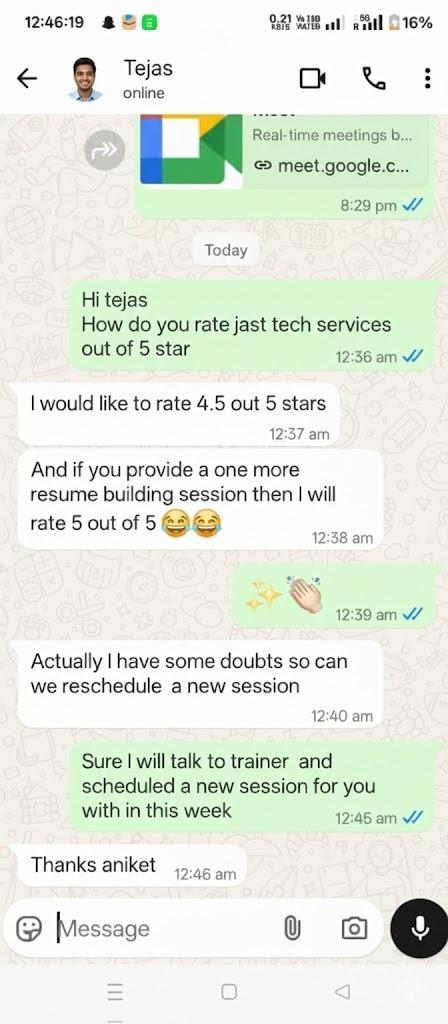
Tejas D.
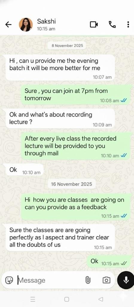
Sakshi
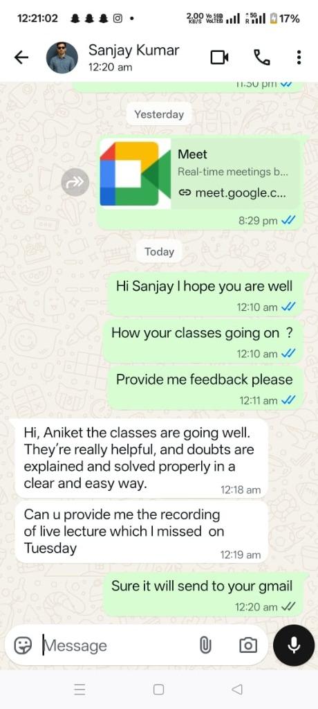
Sanjay Kumar
Specialized Training Programs
JastTech For Corporates
JastTech Courses
Why JastTech is the Best Training Institute?
See how we stand out from the competition
Industry-aligned syllabus covering the complete RTL-to-GDSII flow, floorplanning, CTS, routing, and STA, specifically tailored for the latest semiconductor demands in Chennai.
Outdated syllabi that miss advanced node (7nm/5nm/3nm) challenges and focus mostly on theoretical basics.
100% lab-driven sessions using industry-standard EDA tools to solve actual timing, routing, and congestion issues.
Heavy emphasis on theory with limited tool access or reliance on outdated tools instead of industry standards.
Learn directly from senior physical design engineers and VLSI tape-out experts working in top semiconductor firms.
Taught by trainers with limited recent tape-out experience or purely academic backgrounds.
Work on complex block-level and top-level execution projects from scratch, simulating real tape-out environments to build a strong PD portfolio.
Basic, textbook examples that do not reflect the complexity or scale of modern SoC designs.
Rigorous milestone-based evaluations testing your ability to fix setup/hold violations, IR drop, and DRC/LVS errors.
Generic multiple-choice quizzes that don't test actual EDA tool proficiency or physical design problem-solving.
Dedicated placement assistance, VLSI-specific resume building, and mock technical interviews targeting top semiconductor companies in Chennai and Bengaluru.
Minimal guidance on navigating the highly specialized and technical VLSI interview process.
24/7 dedicated support channels with mentors to help you debug complex tool errors and timing closure roadblocks whenever you need it.
Delayed responses and limited availability of mentors for complex technical debugging.
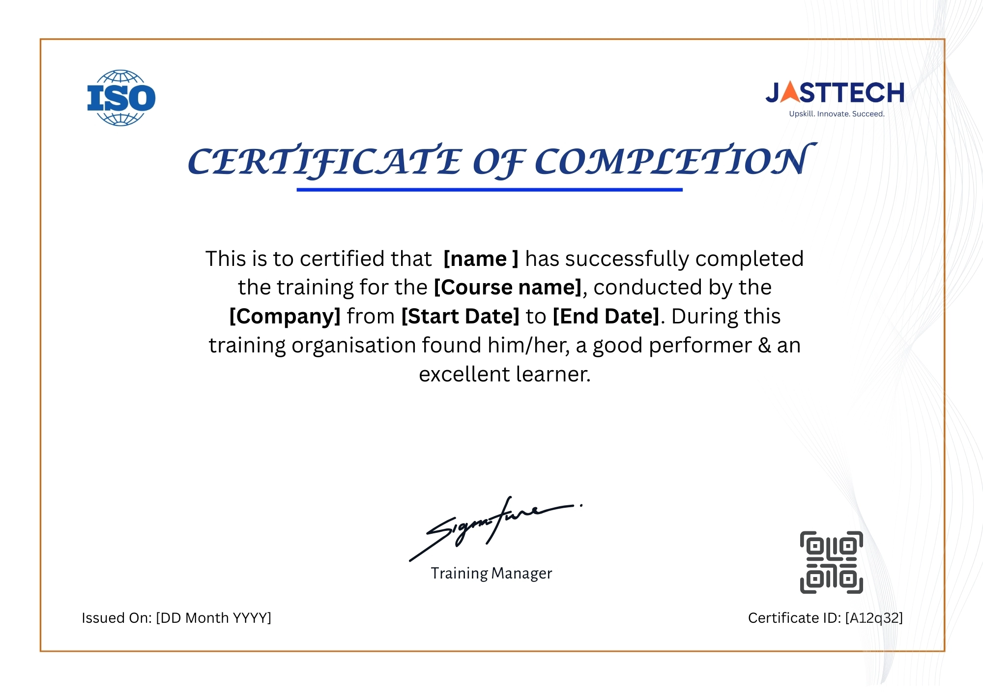
Industry-recognized physical design certification that validates your tape-out capabilities and tool proficiency to top VLSI recruiters.
Generic completion certificates that hold little weight with semiconductor hiring managers.
Lifetime access to updated lecture recordings, PD automation scripts (Tcl/Python), and reference materials to assist you even after securing a job.
Restricted access that expires shortly after the course ends, with extra fees required for renewals.
Premium quality VLSI training at competitive prices, offering flexible payment plans with absolutely no hidden EDA tool-access charges.
Exorbitant fees typical of specialized VLSI courses, or cheaper courses with hidden charges for lab time.
Physical Design Training in Chennai Certification
Prepare
Top Interview Questions
Curated questions with expert answers to help you ace your next interview.
What is the RTL-to-GDSII flow in physical design?
The RTL-to-GDSII flow converts a behavioral hardware description into a manufacturable physical chip layout. It includes synthesis, floorplanning, placement, CTS, routing, physical verification, and final signoff.
What is the difference between floorplanning and placement?
Floorplanning defines the chip's overall structure, including core dimensions, macro locations, and power distribution. Placement assigns standard cells to specific physical locations while optimizing timing, congestion, and area.
What happens when a design has high congestion after placement?
High congestion occurs when routing demand exceeds available routing resources. I would analyze congestion reports, optimize cell placement, adjust floorplan utilization, and reposition macros where necessary.
How do you resolve DRC violations after routing?
I would examine the DRC reports to identify spacing, width, enclosure, or connectivity violations. Then I would correct the affected routes or vias and rerun physical verification to confirm that the violations are resolved.
A design passes placement but fails timing after CTS. How would you debug it?
I would compare pre-CTS and post-CTS timing reports to identify clock insertion delay, skew, and changes in data-path timing. Based on the analysis, I would optimize the clock tree, resize cells, and perform timing-driven optimization.
Support
Frequently Asked FAQs
Can't find what you're looking for? Reach out to our support team anytime.
What is the expected salary after completing Physical Design Training in Chennai?
Freshers entering VLSI physical design roles in India can generally expect ₹3.5–7 LPA, depending on skills, projects, and employer. Experienced professionals may earn ₹8–20 LPA or more based on expertise.
Why should students choose Physical Design Training in Chennai?
Chennai has a strong electronics, semiconductor, automotive, and technology ecosystem. Students can develop practical VLSI skills while exploring opportunities with semiconductor companies and engineering service providers.
Which IT parks and industrial areas in Chennai offer opportunities for physical design professionals?
Important technology and industrial locations include Tidel Park, DLF Cybercity, Ramanujan IT City, Guindy Industrial Estate, Ambattur Industrial Estate, and OMR. These locations support technology, electronics, and engineering-related business activities.
What job roles are available after completing this course in Chennai?
Candidates can pursue roles such as Physical Design Engineer, VLSI Design Engineer, Backend Design Engineer, STA Engineer, Floorplanning Engineer, and Physical Verification Engineer.
Is Physical Design Training in Chennai suitable for freshers?
Yes, the course is suitable for freshers, particularly graduates from ECE, EEE, Electronics, and related engineering branches. It starts with fundamental concepts before progressing to advanced implementation techniques.
The support team was very cooperative and responsive. They made sure all doubts were cleared without delay. Great experience overall.
I had a great experience with the RF Circuit Design course. Thanks to the teaching staff for such a well planned and structured curriculum it really helped me clear my technical certification for my job.
I enrolled in the Post-Silicon Validation Certification Training at JastTech and found it quite different from typical courses. They focus on debugging techniques and real chip-level scenarios, which gave me a better idea of how things work.
One thing I really liked about the Data Analyst course at JastTech is their focus on consistency. Regular sessions and tasks help you stay on track and build a daily learning habit. Also, they provide recordings after live sessions, which help in revision.
I joined JastTech for the DFT course a few months back. At first, I wasn’t sure what to expect, but the classes turned out to be really helpful. The teaching is simple and not too complicated, which helped me keep up.
Take the Next Step in Your Career
Join thousands of learners who have upgraded their skills with our industry-focused training programs. Our experts are here to guide you every step of the way.
Related Articles & Insights
Deep dive into Physical Design Training in Chennai with our expert-curated technical guides and industry updates.

Understanding Industry Expectations for Physical Design Engineers: Insights from JastTech
Discover what semiconductor companies expect from physical design engineers. Explore essential VLSI skills, industry tools, timing closure, PPA optimization, and practical career preparation with insights from JastTech.

Physical Design vs Physical Verification: Roles, Skills and Career Opportunities
New on the JastTech blog: Physical Design vs Physical Verification. It covers what each VLSI role does, the skills and tools they need, and the career paths, so you can choose the right one.

How to Clear Your First Physical Design Interview: A Step-by-Step Roadmap
Preparing for your first Physical Design interview? Explore this step-by-step roadmap covering CMOS fundamentals, digital logic, setup and hold timing, floorplanning, placement, CTS, routing, timing closure, power, congestion, EDA tools, Tcl scripting, and project preparation.

Physical Design Engineer vs. STA Engineer: Responsibilities, Skills, and Career Growth
Physical Design Engineer vs STA Engineer: what each role does, the skills and tools they need, how they work together on timing closure, and how to choose your VLSI career path.
We're Here to Help –
Reach Our Global Offices
Hyderabad
JastTech
Training & Development Center
91 Springboard Business Hub ,Madhapur LVS Arcade, 71, Jubilee Enclave, HITEC City, Hyderabad,India Telangana 500081
Pune
JastTech
Training & Development Center
Sr. No. 30/2/1, 3rd Floor, Above Rajrshi Shahu Bank & BOB Balaji Nagar, Dhankawadi, Katraj, Pune, Maharashtra 411043
Noida
JastTech
Training & Development Center
B 8, B Block, Sector 2, Noida, Metro Station Rd, near sector 15 Metro, Uttar Pradesh 201301
Hyderabad
JastTech
Training & Development Center
91 Springboard Business Hub ,Madhapur LVS Arcade, 71, Jubilee Enclave, HITEC City, Hyderabad,India Telangana 500081
Pune
JastTech
Training & Development Center
Sr. No. 30/2/1, 3rd Floor, Above Rajrshi Shahu Bank & BOB Balaji Nagar, Dhankawadi, Katraj, Pune, Maharashtra 411043
Noida
JastTech
Training & Development Center
B 8, B Block, Sector 2, Noida, Metro Station Rd, near sector 15 Metro, Uttar Pradesh 201301
Can't find a JastTech location near you? Contact us for more information.